EP0543490A1 - Dispositif pour l'accordement adaptif à un signal périodique reçu - Google Patents
Dispositif pour l'accordement adaptif à un signal périodique reçu Download PDFInfo
- Publication number
- EP0543490A1 EP0543490A1 EP92309125A EP92309125A EP0543490A1 EP 0543490 A1 EP0543490 A1 EP 0543490A1 EP 92309125 A EP92309125 A EP 92309125A EP 92309125 A EP92309125 A EP 92309125A EP 0543490 A1 EP0543490 A1 EP 0543490A1
- Authority
- EP
- European Patent Office
- Prior art keywords
- signal
- delayed
- output signal
- received
- input
- Prior art date
- Legal status (The legal status is an assumption and is not a legal conclusion. Google has not performed a legal analysis and makes no representation as to the accuracy of the status listed.)
- Granted
Links
Images

Classifications
-
- H—ELECTRICITY
- H04—ELECTRIC COMMUNICATION TECHNIQUE
- H04Q—SELECTING
- H04Q1/00—Details of selecting apparatus or arrangements
- H04Q1/18—Electrical details
- H04Q1/30—Signalling arrangements; Manipulation of signalling currents
- H04Q1/44—Signalling arrangements; Manipulation of signalling currents using alternate current
- H04Q1/444—Signalling arrangements; Manipulation of signalling currents using alternate current with voice-band signalling frequencies
- H04Q1/45—Signalling arrangements; Manipulation of signalling currents using alternate current with voice-band signalling frequencies using multi-frequency signalling
- H04Q1/457—Signalling arrangements; Manipulation of signalling currents using alternate current with voice-band signalling frequencies using multi-frequency signalling with conversion of multifrequency signals into digital signals
- H04Q1/4575—Signalling arrangements; Manipulation of signalling currents using alternate current with voice-band signalling frequencies using multi-frequency signalling with conversion of multifrequency signals into digital signals which are transmitted in digital form
Definitions
- the present invention is directed to an apparatus which will adaptively tune to a received periodic signal and, in one embodiment, will identify the frequency of the received signal to a user.
- Adaptive tuning to a received periodic signal is useful in a variety of situations, such as identifying frequency of a fire control or a search radar of a weapon system, tuning to a homing beacon or other similar navigational device, or, generally, tuning to or identifying any periodic signal of unknown frequency with speed and precision.
- Prior art devices for identifying and tuning to an unidentified (i.e., the frequency is unknown) received signal involved filtering the received signal through an array of high Q filters, and establishing a frequency range within which the received frequency is propagated by noting which of the high Q filters in the array passes the received signal.
- Such prior art circuits must necessarily have a large number of high Q filters in the filter array. A greater number of filters reduces the interval between detectable frequencies and, therefore, increased the accuracy by which the received frequency can be determined.
- an apparatus for detection of frequency of a received signal which is stable in operation in a variety of environments, which is capable of accurate determination of the frequency of the received signal, and which is capable of ascertaining the frequency of the received signal speedily.
- the apparatus preferably employs digital signal processing techniques for algorithmic generation of a sinusoidal estimated output signal, determines the difference between the estimated output signal and the received signal, and generates an error signal based upon the difference between the estimated output signal and the received signal.
- the error signal is applied to vary at least one factor of the algorithmic determination of the estimated output signal appropriately to reduce the error between the estimated output signal and the received signal.
- the algorithmic factor which was varied to effect reduction of the error signal is logically treated to ascertain the frequency of the received signal and such information is conveyed to a user.
- An alternative embodiment of the invention accommodates white Gaussian noise in tuning to a received signal.
- the apparatus is inexpensive to construct and ascertains the frequency of a received signal both speedily and with a high degree of accuracy.
- a second summing circuit 42 receives estimated signal est. x n+1 at a negative input terminal 46, receives received signal x n+1 at an input 44, and generates an output signal at an output 48.
- the output signal generated at output 48 is an error signal ⁇ which comprises the difference between received signal x n+1 , less estimated signal est. x n+1 .
- Error signal ⁇ is applied to an input 50 of multiplier source 28.
- Multiplier source 28 responds to error signal ⁇ to alter multiplier K provided to multiplier input 26 appropriately to reduce error signal ⁇ .
- Adaptive tuning apparatus 10 also may include a logic module 54 which receives an input signal from multiplier source 28 at an input 56.
- the input received from multiplier source 28 at input 56 comprises the value of K generated by multiplier source 28 when error signal ⁇ equals Zero.
- logic module 54 will contain a stored arccosine table in appropriate detail to identify, with the accuracy desired, the arccosine of the quantity: K 2 Further, logic module 54 stores the value f s of the sampling frequency and the value ⁇ to enable calculation of f t , the target frequency, according to Eqn. [7] above.
- Fig. 2 is a schematic diagram of an alternate embodiment of the present invention configured to accommodate noise.
- Eqn. [3], discussed in connection with the preferred embodiment of the present invention illustrated in Fig. 1, may be rewritten to account for white Gaussian noise in the form: where f(n) equals a time varying frequency of the received sinusoidal signal and f s equals sampling frequency.
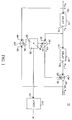
- an apparatus 100 having a first delay circuit 102 and a second delay circuit 104.
- An input signal, x(n) is received by apparatus 100 at an input 106 to first delay circuit 102.
- First delay circuit 102 delays input signal x(n) one clock period and generates at an output 108 a once-delayed signal x(n-1);
- x(n-1) is substantially input signal x(n) delayed one clock period.
- Second delay circuit 104 receives once-delayed signal x(n-1) at an input 110 and delays once-delayed signal x(n-1) by one further clock period, generating at a twice-delayed signal x(n-2) at an output 112.
- Once-delayed signal x(n-1) is also applied to a multiplier 114 at an input 116.
- a first weighted factor source 118 provides a first weighted factor, W1(n), to an input 120 of multiplier 114.
- Multiplier 114 generates at an output 122 a weighted once-delayed signal which is substantially the product of once-delayed signal x(n-1) and first weighted factor W1(n). This weighted once-delayed signal is applied to an input 124 of a summing node 126.
- Twice-delayed signal x(n-2) is applied to an input 128 of a multiplier 130.
- Multiplier 130 also receives at an input 132 a second weighted factor, W2(n), from a second weighted factor source 134.
- Summing node 126 produces at an output 136 an estimation of input signal x(n), x ⁇ (n), estimated input signal x ⁇ (n) is applied to an input 138 of a summing node 140. Also received by summing node 140 at an input 142 is input signal x(n).
- Summing node 140 produces at an output 144 an error signal ⁇ .
- First weighted factor source 118 and second weighted factor source 134 are responsive to error signal ⁇ to vary first weighted factor W1(n) and second weighted factor W2(n) appropriately to reduce error signal ⁇ . That is, W1(n) and W2(n) are appropriately varied to reduce the difference between input signal x(n) and estimated input signal x ⁇ (n). As may be seen from inspection of Fig.
- x ⁇ (n) W1(n-1)x(n-1)+W2(n-1)x(n-2) [9]
- W2(n) W2(n-1)+ ⁇ (n)x(n-2) [11]
- W1(n-1) W1(n-2)+ ⁇ (n-1)x(n-2) [14b]
- W1(n) W1(n-2)+ ⁇ [ ⁇ (n)x(n-1)+ ⁇ (n-1)x(n-2) [14c]
- W1(m) W1(m)+ ⁇ [ ⁇ (n)x(n-1)+ ⁇ (n-1)x(n-2)+...+ ⁇ (m+1)x(m)] [14d] Therefore:
- Threshold circuit 166 is preferably designed to substantially implement the approximations represented by Eqn. [37] above, so that the signal, "A”, provided by threshold circuit 166 at its output 168 is variable, as indicated in the table associated with Fig. 2, according to the value of signal W1(n) received at input 164.
- the output signal provided by threshold circuit 166 is applied to an input 170 of multiplier 160 so that multiplier 160 provides at its output 172 a signal "B".
- Signal "B” varies as indicated in the table associated with Fig. 2, depending upon the value of W1(n) received at input 164 of threshold circuit 166.
- Signal "B” is applied to an input 174 of a summing node 176; the signal W1(n) is provided to a second input 178 of summing node 176 from first weighted factor source 118, and summing node 176 provides at its output 180 the value W1*.
- signal W1* is calculated by frequency identification circuit 150 in accordance with Eqn. [37] above.
- the value provided at output 180 of summing node 176 uniquely identifies the frequency of the sinusoidal signal, x s (n), received at input 106 of delay circuit 102 through a look-up table or similar arrangement in a logic circuit (not shown in Fig. 2).
- a second weighted factor, W2(n) is employed to estimate noise energy in the received signal x(n) and second weighted factor W2(n) is employed to apply a correction to first weighted factor W1(n) in order to accurately reflect an index uniquely identifying the sinusoidal wave form x s (n) contained within the received signal x n , which is received in the form of Eqn.
Landscapes
- Engineering & Computer Science (AREA)
- Computer Networks & Wireless Communication (AREA)
- Noise Elimination (AREA)
- Circuits Of Receivers In General (AREA)
- Channel Selection Circuits, Automatic Tuning Circuits (AREA)
- Measurement Of Resistance Or Impedance (AREA)
- Measuring Frequencies, Analyzing Spectra (AREA)
- Superheterodyne Receivers (AREA)
Applications Claiming Priority (2)
| Application Number | Priority Date | Filing Date | Title |
|---|---|---|---|
| US07/796,318 US5339251A (en) | 1991-11-22 | 1991-11-22 | Apparatus for adaptively tuning to a received periodic signal |
| US796318 | 1991-11-22 |
Publications (2)
| Publication Number | Publication Date |
|---|---|
| EP0543490A1 true EP0543490A1 (fr) | 1993-05-26 |
| EP0543490B1 EP0543490B1 (fr) | 1997-07-23 |
Family
ID=25167903
Family Applications (1)
| Application Number | Title | Priority Date | Filing Date |
|---|---|---|---|
| EP92309125A Expired - Lifetime EP0543490B1 (fr) | 1991-11-22 | 1992-10-07 | Dispositif pour l'accordement adaptif à un signal périodique reçu |
Country Status (6)
| Country | Link |
|---|---|
| US (1) | US5339251A (fr) |
| EP (1) | EP0543490B1 (fr) |
| JP (1) | JPH0677773A (fr) |
| AT (1) | ATE155951T1 (fr) |
| DE (1) | DE69221081T2 (fr) |
| ES (1) | ES2103896T3 (fr) |
Families Citing this family (1)
| Publication number | Priority date | Publication date | Assignee | Title |
|---|---|---|---|---|
| US20020133391A1 (en) * | 2001-03-12 | 2002-09-19 | Johnson Timothy Lee | Marketing systems and methods |
Citations (2)
| Publication number | Priority date | Publication date | Assignee | Title |
|---|---|---|---|---|
| GB2100537A (en) * | 1981-06-15 | 1982-12-22 | Western Electric Co | Adaptive techniques for automatic frequency determination and measurement |
| EP0300265A2 (fr) * | 1987-07-24 | 1989-01-25 | Advanced Micro Devices, Inc. | Procédé de détection numérique de tonalités |
Family Cites Families (4)
| Publication number | Priority date | Publication date | Assignee | Title |
|---|---|---|---|---|
| US4438504A (en) * | 1981-06-15 | 1984-03-20 | Bell Telephone Laboratories, Incorporated | Adaptive techniques for automatic frequency determination and measurement |
| US4433422A (en) * | 1982-03-29 | 1984-02-21 | Sperry Corporation | Frequency measuring system for alternating frequency signals |
| US4791390A (en) * | 1982-07-01 | 1988-12-13 | Sperry Corporation | MSE variable step adaptive filter |
| US5189381A (en) * | 1991-10-31 | 1993-02-23 | Advanced Micro Devices, Inc. | Apparatus for generating a sinusoidal output signal |
-
1991
- 1991-11-22 US US07/796,318 patent/US5339251A/en not_active Expired - Lifetime
-
1992
- 1992-10-07 EP EP92309125A patent/EP0543490B1/fr not_active Expired - Lifetime
- 1992-10-07 DE DE69221081T patent/DE69221081T2/de not_active Expired - Fee Related
- 1992-10-07 ES ES92309125T patent/ES2103896T3/es not_active Expired - Lifetime
- 1992-10-07 AT AT92309125T patent/ATE155951T1/de not_active IP Right Cessation
- 1992-11-20 JP JP4312348A patent/JPH0677773A/ja not_active Withdrawn
Patent Citations (2)
| Publication number | Priority date | Publication date | Assignee | Title |
|---|---|---|---|---|
| GB2100537A (en) * | 1981-06-15 | 1982-12-22 | Western Electric Co | Adaptive techniques for automatic frequency determination and measurement |
| EP0300265A2 (fr) * | 1987-07-24 | 1989-01-25 | Advanced Micro Devices, Inc. | Procédé de détection numérique de tonalités |
Also Published As
| Publication number | Publication date |
|---|---|
| DE69221081T2 (de) | 1998-02-12 |
| US5339251A (en) | 1994-08-16 |
| ATE155951T1 (de) | 1997-08-15 |
| DE69221081D1 (de) | 1997-09-04 |
| JPH0677773A (ja) | 1994-03-18 |
| ES2103896T3 (es) | 1997-10-01 |
| EP0543490B1 (fr) | 1997-07-23 |
Similar Documents
| Publication | Publication Date | Title |
|---|---|---|
| US4216463A (en) | Programmable digital tone detector | |
| US4438504A (en) | Adaptive techniques for automatic frequency determination and measurement | |
| US4660215A (en) | Transmitter/receiver system | |
| US4075703A (en) | Recursive filter mean-level detector | |
| US3877011A (en) | Dual channel adaptable moving target processor | |
| US4403298A (en) | Adaptive techniques for automatic frequency determination and measurement | |
| US4633426A (en) | Method and apparatus for detecting a binary convoluted coded signal | |
| US3833797A (en) | Statistical noise processor | |
| EP0622963A2 (fr) | Dispositif pour l'accordement adaptif à un signal périodique reçu | |
| EP0543490B1 (fr) | Dispositif pour l'accordement adaptif à un signal périodique reçu | |
| JP2681105B2 (ja) | 周期波形の発生方法 | |
| US3484746A (en) | Adaptive pattern recognition system | |
| KR19990057712A (ko) | 디지털 신호 처리장치 및 그 방법 | |
| US5377131A (en) | Digital amplitude estimator | |
| US5179529A (en) | High speed fourier transform engine | |
| WO1991010913A1 (fr) | Procede et appareil detecteur de salves a frequence coherente | |
| US5694435A (en) | Digital method of detecting pulses of short duration and arrangement for implementing the method | |
| USH292H (en) | Apparatus for the detection of angles-of-arrival of radio frequency signals | |
| RU97113716A (ru) | Система управления огнем | |
| RU2137142C1 (ru) | Способ измерения закона перестройки несущей частоты радиоимпульсов с частотной модуляцией и устройство для его осуществления | |
| SU1510089A1 (ru) | Способ знаковой дельта-модул ции и устройство дл его осуществлени | |
| Blomqvist | Figures of merit of windows for power density spectrum estimation with the DFT | |
| SU1109768A1 (ru) | Устройство дл определени формы случайного сигнала | |
| RU1803920C (ru) | Устройство дл вычислени спектра сигналов | |
| RU2238612C2 (ru) | Адаптивный способ обнаружения и распознавания синхросигнала и устройство для его осуществления |
Legal Events
| Date | Code | Title | Description |
|---|---|---|---|
| PUAI | Public reference made under article 153(3) epc to a published international application that has entered the european phase |
Free format text: ORIGINAL CODE: 0009012 |
|
| AK | Designated contracting states |
Kind code of ref document: A1 Designated state(s): AT BE CH DE DK ES FR GB GR IE IT LI LU MC NL PT SE |
|
| 17P | Request for examination filed |
Effective date: 19931028 |
|
| 17Q | First examination report despatched |
Effective date: 19960508 |
|
| GRAG | Despatch of communication of intention to grant |
Free format text: ORIGINAL CODE: EPIDOS AGRA |
|
| GRAH | Despatch of communication of intention to grant a patent |
Free format text: ORIGINAL CODE: EPIDOS IGRA |
|
| GRAH | Despatch of communication of intention to grant a patent |
Free format text: ORIGINAL CODE: EPIDOS IGRA |
|
| GRAA | (expected) grant |
Free format text: ORIGINAL CODE: 0009210 |
|
| AK | Designated contracting states |
Kind code of ref document: B1 Designated state(s): AT BE CH DE DK ES FR GB GR IE IT LI LU MC NL PT SE |
|
| PG25 | Lapsed in a contracting state [announced via postgrant information from national office to epo] |
Ref country code: NL Free format text: LAPSE BECAUSE OF FAILURE TO SUBMIT A TRANSLATION OF THE DESCRIPTION OR TO PAY THE FEE WITHIN THE PRESCRIBED TIME-LIMIT Effective date: 19970723 Ref country code: LI Effective date: 19970723 Ref country code: IT Free format text: LAPSE BECAUSE OF FAILURE TO SUBMIT A TRANSLATION OF THE DESCRIPTION OR TO PAY THE FEE WITHIN THE PRE;WARNING: LAPSES OF ITALIAN PATENTS WITH EFFECTIVE DATE BEFORE 2007 MAY HAVE OCCURRED AT ANY TIME BEFORE 2007. THE CORRECT EFFECTIVE DATE MAY BE DIFFERENT FROM THE ONE RECORDED.SCRIBED TIME-LIMIT Effective date: 19970723 Ref country code: GR Free format text: LAPSE BECAUSE OF FAILURE TO SUBMIT A TRANSLATION OF THE DESCRIPTION OR TO PAY THE FEE WITHIN THE PRESCRIBED TIME-LIMIT Effective date: 19970723 Ref country code: DK Effective date: 19970723 Ref country code: CH Effective date: 19970723 Ref country code: AT Effective date: 19970723 |
|
| REF | Corresponds to: |
Ref document number: 155951 Country of ref document: AT Date of ref document: 19970815 Kind code of ref document: T |
|
| REG | Reference to a national code |
Ref country code: CH Ref legal event code: EP |
|
| ET | Fr: translation filed | ||
| REF | Corresponds to: |
Ref document number: 69221081 Country of ref document: DE Date of ref document: 19970904 |
|
| REG | Reference to a national code |
Ref country code: ES Ref legal event code: FG2A Ref document number: 2103896 Country of ref document: ES Kind code of ref document: T3 |
|
| PG25 | Lapsed in a contracting state [announced via postgrant information from national office to epo] |
Ref country code: IE Free format text: LAPSE BECAUSE OF NON-PAYMENT OF DUE FEES Effective date: 19971007 |
|
| PG25 | Lapsed in a contracting state [announced via postgrant information from national office to epo] |
Ref country code: SE Effective date: 19971023 |
|
| PG25 | Lapsed in a contracting state [announced via postgrant information from national office to epo] |
Ref country code: PT Effective date: 19971028 |
|
| PG25 | Lapsed in a contracting state [announced via postgrant information from national office to epo] |
Ref country code: LU Free format text: LAPSE BECAUSE OF NON-PAYMENT OF DUE FEES Effective date: 19971031 |
|
| NLV1 | Nl: lapsed or annulled due to failure to fulfill the requirements of art. 29p and 29m of the patents act | ||
| REG | Reference to a national code |
Ref country code: CH Ref legal event code: PL |
|
| PGFP | Annual fee paid to national office [announced via postgrant information from national office to epo] |
Ref country code: BE Payment date: 19980209 Year of fee payment: 6 |
|
| PG25 | Lapsed in a contracting state [announced via postgrant information from national office to epo] |
Ref country code: MC Free format text: LAPSE BECAUSE OF NON-PAYMENT OF DUE FEES Effective date: 19980430 |
|
| PLBE | No opposition filed within time limit |
Free format text: ORIGINAL CODE: 0009261 |
|
| 26N | No opposition filed | ||
| PG25 | Lapsed in a contracting state [announced via postgrant information from national office to epo] |
Ref country code: BE Free format text: LAPSE BECAUSE OF NON-PAYMENT OF DUE FEES Effective date: 19981031 |
|
| BERE | Be: lapsed |
Owner name: ADVANCED MICRO DEVICES INC. Effective date: 19981031 |
|
| PGFP | Annual fee paid to national office [announced via postgrant information from national office to epo] |
Ref country code: ES Payment date: 19991014 Year of fee payment: 8 |
|
| PGFP | Annual fee paid to national office [announced via postgrant information from national office to epo] |
Ref country code: GB Payment date: 20000918 Year of fee payment: 9 |
|
| PG25 | Lapsed in a contracting state [announced via postgrant information from national office to epo] |
Ref country code: ES Free format text: LAPSE BECAUSE OF NON-PAYMENT OF DUE FEES Effective date: 20001008 |
|
| PGFP | Annual fee paid to national office [announced via postgrant information from national office to epo] |
Ref country code: FR Payment date: 20001009 Year of fee payment: 9 |
|
| PG25 | Lapsed in a contracting state [announced via postgrant information from national office to epo] |
Ref country code: GB Free format text: LAPSE BECAUSE OF NON-PAYMENT OF DUE FEES Effective date: 20011007 |
|
| REG | Reference to a national code |
Ref country code: GB Ref legal event code: IF02 |
|
| GBPC | Gb: european patent ceased through non-payment of renewal fee |
Effective date: 20011007 |
|
| PG25 | Lapsed in a contracting state [announced via postgrant information from national office to epo] |
Ref country code: FR Free format text: LAPSE BECAUSE OF NON-PAYMENT OF DUE FEES Effective date: 20020628 |
|
| REG | Reference to a national code |
Ref country code: FR Ref legal event code: ST |
|
| PGFP | Annual fee paid to national office [announced via postgrant information from national office to epo] |
Ref country code: DE Payment date: 20021031 Year of fee payment: 11 |
|
| REG | Reference to a national code |
Ref country code: ES Ref legal event code: FD2A Effective date: 20011113 |
|
| PG25 | Lapsed in a contracting state [announced via postgrant information from national office to epo] |
Ref country code: DE Free format text: LAPSE BECAUSE OF NON-PAYMENT OF DUE FEES Effective date: 20040501 |