EP0545363A1 - Procédé de fabrication d'un circuit intégré et structure - Google Patents
Procédé de fabrication d'un circuit intégré et structure Download PDFInfo
- Publication number
- EP0545363A1 EP0545363A1 EP92120493A EP92120493A EP0545363A1 EP 0545363 A1 EP0545363 A1 EP 0545363A1 EP 92120493 A EP92120493 A EP 92120493A EP 92120493 A EP92120493 A EP 92120493A EP 0545363 A1 EP0545363 A1 EP 0545363A1
- Authority
- EP
- European Patent Office
- Prior art keywords
- resistor
- definition
- region
- pwell
- mask
- Prior art date
- Legal status (The legal status is an assumption and is not a legal conclusion. Google has not performed a legal analysis and makes no representation as to the accuracy of the status listed.)
- Withdrawn
Links
Images





Classifications
-
- H—ELECTRICITY
- H10—SEMICONDUCTOR DEVICES; ELECTRIC SOLID-STATE DEVICES NOT OTHERWISE PROVIDED FOR
- H10D—INORGANIC ELECTRIC SEMICONDUCTOR DEVICES
- H10D1/00—Resistors, capacitors or inductors
- H10D1/01—Manufacture or treatment
- H10D1/025—Manufacture or treatment of resistors having potential barriers
-
- H—ELECTRICITY
- H10—SEMICONDUCTOR DEVICES; ELECTRIC SOLID-STATE DEVICES NOT OTHERWISE PROVIDED FOR
- H10D—INORGANIC ELECTRIC SEMICONDUCTOR DEVICES
- H10D84/00—Integrated devices formed in or on semiconductor substrates that comprise only semiconducting layers, e.g. on Si wafers or on GaAs-on-Si wafers
- H10D84/01—Manufacture or treatment
- H10D84/0123—Integrating together multiple components covered by H10D12/00 or H10D30/00, e.g. integrating multiple IGBTs
- H10D84/0126—Integrating together multiple components covered by H10D12/00 or H10D30/00, e.g. integrating multiple IGBTs the components including insulated gates, e.g. IGFETs
- H10D84/0165—Integrating together multiple components covered by H10D12/00 or H10D30/00, e.g. integrating multiple IGBTs the components including insulated gates, e.g. IGFETs the components including complementary IGFETs, e.g. CMOS devices
- H10D84/0191—Manufacturing their doped wells
-
- H—ELECTRICITY
- H10—SEMICONDUCTOR DEVICES; ELECTRIC SOLID-STATE DEVICES NOT OTHERWISE PROVIDED FOR
- H10D—INORGANIC ELECTRIC SEMICONDUCTOR DEVICES
- H10D84/00—Integrated devices formed in or on semiconductor substrates that comprise only semiconducting layers, e.g. on Si wafers or on GaAs-on-Si wafers
- H10D84/01—Manufacture or treatment
- H10D84/0107—Integrating at least one component covered by H10D12/00 or H10D30/00 with at least one component covered by H10D8/00, H10D10/00 or H10D18/00, e.g. integrating IGFETs with BJTs
- H10D84/0109—Integrating at least one component covered by H10D12/00 or H10D30/00 with at least one component covered by H10D8/00, H10D10/00 or H10D18/00, e.g. integrating IGFETs with BJTs the at least one component covered by H10D12/00 or H10D30/00 being a MOS device
-
- H—ELECTRICITY
- H10—SEMICONDUCTOR DEVICES; ELECTRIC SOLID-STATE DEVICES NOT OTHERWISE PROVIDED FOR
- H10D—INORGANIC ELECTRIC SEMICONDUCTOR DEVICES
- H10D84/00—Integrated devices formed in or on semiconductor substrates that comprise only semiconducting layers, e.g. on Si wafers or on GaAs-on-Si wafers
- H10D84/01—Manufacture or treatment
- H10D84/0123—Integrating together multiple components covered by H10D12/00 or H10D30/00, e.g. integrating multiple IGBTs
- H10D84/0126—Integrating together multiple components covered by H10D12/00 or H10D30/00, e.g. integrating multiple IGBTs the components including insulated gates, e.g. IGFETs
- H10D84/0165—Integrating together multiple components covered by H10D12/00 or H10D30/00, e.g. integrating multiple IGBTs the components including insulated gates, e.g. IGFETs the components including complementary IGFETs, e.g. CMOS devices
- H10D84/0167—Manufacturing their channels
-
- H—ELECTRICITY
- H10—SEMICONDUCTOR DEVICES; ELECTRIC SOLID-STATE DEVICES NOT OTHERWISE PROVIDED FOR
- H10D—INORGANIC ELECTRIC SEMICONDUCTOR DEVICES
- H10D84/00—Integrated devices formed in or on semiconductor substrates that comprise only semiconducting layers, e.g. on Si wafers or on GaAs-on-Si wafers
- H10D84/01—Manufacture or treatment
- H10D84/0123—Integrating together multiple components covered by H10D12/00 or H10D30/00, e.g. integrating multiple IGBTs
- H10D84/0126—Integrating together multiple components covered by H10D12/00 or H10D30/00, e.g. integrating multiple IGBTs the components including insulated gates, e.g. IGFETs
- H10D84/0165—Integrating together multiple components covered by H10D12/00 or H10D30/00, e.g. integrating multiple IGBTs the components including insulated gates, e.g. IGFETs the components including complementary IGFETs, e.g. CMOS devices
- H10D84/017—Manufacturing their source or drain regions, e.g. silicided source or drain regions
-
- H—ELECTRICITY
- H10—SEMICONDUCTOR DEVICES; ELECTRIC SOLID-STATE DEVICES NOT OTHERWISE PROVIDED FOR
- H10D—INORGANIC ELECTRIC SEMICONDUCTOR DEVICES
- H10D84/00—Integrated devices formed in or on semiconductor substrates that comprise only semiconducting layers, e.g. on Si wafers or on GaAs-on-Si wafers
- H10D84/01—Manufacture or treatment
- H10D84/02—Manufacture or treatment characterised by using material-based technologies
- H10D84/03—Manufacture or treatment characterised by using material-based technologies using Group IV technology, e.g. silicon technology or silicon-carbide [SiC] technology
- H10D84/038—Manufacture or treatment characterised by using material-based technologies using Group IV technology, e.g. silicon technology or silicon-carbide [SiC] technology using silicon technology, e.g. SiGe
-
- H—ELECTRICITY
- H10—SEMICONDUCTOR DEVICES; ELECTRIC SOLID-STATE DEVICES NOT OTHERWISE PROVIDED FOR
- H10D—INORGANIC ELECTRIC SEMICONDUCTOR DEVICES
- H10D84/00—Integrated devices formed in or on semiconductor substrates that comprise only semiconducting layers, e.g. on Si wafers or on GaAs-on-Si wafers
- H10D84/80—Integrated devices formed in or on semiconductor substrates that comprise only semiconducting layers, e.g. on Si wafers or on GaAs-on-Si wafers characterised by the integration of at least one component covered by groups H10D12/00 or H10D30/00, e.g. integration of IGFETs
- H10D84/82—Integrated devices formed in or on semiconductor substrates that comprise only semiconducting layers, e.g. on Si wafers or on GaAs-on-Si wafers characterised by the integration of at least one component covered by groups H10D12/00 or H10D30/00, e.g. integration of IGFETs of only field-effect components
- H10D84/83—Integrated devices formed in or on semiconductor substrates that comprise only semiconducting layers, e.g. on Si wafers or on GaAs-on-Si wafers characterised by the integration of at least one component covered by groups H10D12/00 or H10D30/00, e.g. integration of IGFETs of only field-effect components of only insulated-gate FETs [IGFET]
- H10D84/85—Complementary IGFETs, e.g. CMOS
-
- H—ELECTRICITY
- H10—SEMICONDUCTOR DEVICES; ELECTRIC SOLID-STATE DEVICES NOT OTHERWISE PROVIDED FOR
- H10D—INORGANIC ELECTRIC SEMICONDUCTOR DEVICES
- H10D84/00—Integrated devices formed in or on semiconductor substrates that comprise only semiconducting layers, e.g. on Si wafers or on GaAs-on-Si wafers
- H10D84/80—Integrated devices formed in or on semiconductor substrates that comprise only semiconducting layers, e.g. on Si wafers or on GaAs-on-Si wafers characterised by the integration of at least one component covered by groups H10D12/00 or H10D30/00, e.g. integration of IGFETs
- H10D84/811—Combinations of field-effect devices and one or more diodes, capacitors or resistors
- H10D84/817—Combinations of field-effect devices and resistors only
-
- H—ELECTRICITY
- H10—SEMICONDUCTOR DEVICES; ELECTRIC SOLID-STATE DEVICES NOT OTHERWISE PROVIDED FOR
- H10D—INORGANIC ELECTRIC SEMICONDUCTOR DEVICES
- H10D84/00—Integrated devices formed in or on semiconductor substrates that comprise only semiconducting layers, e.g. on Si wafers or on GaAs-on-Si wafers
- H10D84/80—Integrated devices formed in or on semiconductor substrates that comprise only semiconducting layers, e.g. on Si wafers or on GaAs-on-Si wafers characterised by the integration of at least one component covered by groups H10D12/00 or H10D30/00, e.g. integration of IGFETs
- H10D84/82—Integrated devices formed in or on semiconductor substrates that comprise only semiconducting layers, e.g. on Si wafers or on GaAs-on-Si wafers characterised by the integration of at least one component covered by groups H10D12/00 or H10D30/00, e.g. integration of IGFETs of only field-effect components
- H10D84/83—Integrated devices formed in or on semiconductor substrates that comprise only semiconducting layers, e.g. on Si wafers or on GaAs-on-Si wafers characterised by the integration of at least one component covered by groups H10D12/00 or H10D30/00, e.g. integration of IGFETs of only field-effect components of only insulated-gate FETs [IGFET]
- H10D84/85—Complementary IGFETs, e.g. CMOS
- H10D84/859—Complementary IGFETs, e.g. CMOS comprising both N-type and P-type wells, e.g. twin-tub
Definitions
- This invention relates to a new high definition, high resistance resistor structure that may be coupled to integrated circuit structures. More particularly, the invention is applicable to CMOS and BICMOS transistor structures and provides a new process for fabrication of new CMOS and BICMOS integrated circuit structures that include the new resistor structure.
- the invention uses selected mask sequences from the CMOS transistor structure fabrication steps with modification of the masks according to the invention to form the new resistor structure.
- CMOS transistor structures including BICMOS structures
- the respective gates are used for self-alignment of corresponding sources and drains. It is a goal to provide tight control of the dimensions of these structures and to minimize dimensions to the greatest extent possible. Furthermore, it is a goal to place active elements at or near the surface of the structure. In many cases, it is desirable to utilize a resistor in connection with integrated circuit structures in order to enhance circuit design capability.
- CMOS transistor structures combining complementary NMOS and PMOS transistor structures, are fabricated, for example, on a P type substrate of semiconductor material by first forming a PWell and an NWell using conventional mask, etch and implant sequences.
- An N+ concentration of relatively fast diffusing N type atoms is implanted to form an NWell "bed” and a P+ concentration of relatively fast diffusing P type atoms is implanted to form a PWell "bed.”
- An epitaxial layer in the form of a single crystal N type semiconductor material is then deposited over both the NWell and the PWell. Both wells are then retrograde-diffused to the surface of the epitaxial layer by conventional diffusion processing means. Isolation oxide layers are formed about the CMOS transistor structure by conventional mask, etch and formation sequences so as to isolate the CMOS from adjacent structures. The transistor structure is also framed by field oxide regions formed at the upper surface of the isolation regions using a field oxide region definition mask. P type channel stop layers formed at the same time as the PWell, underlie the isolation oxide regions contacting both the NWell and PWell. The channel stop regions act to isolate the wells from parasitic MOS effects caused by adjacent structures.
- CMOS transistor structure requires the introduction of a gate, a source, and a drain to the NMOS and PMOS elements of the complementary transistor structure.
- the gates may be formed of a polycrystalline layer of semiconductor material, using a conventional mask, etch and deposition sequence. These poly gates are located above the source, drain and channel regions of each well. The poly gates are isolated from the channel regions by a gate oxide layer.
- the gate is formed of polycrystalline silicon because that material can withstand subsequent annealing temperatures on the order of 1000-1100°C and the gate can therefore be used to accurately align the transistor's source and drain contacts.
- the source and drain regions are preliminarily formed and defined by first implanting a relatively fast-diffusing N type atom using conventional mask, etch and implant sequences.
- a gate definition mask opening in the polycrystalline layer defines the location of the shallow source and drain regions, which are separated by the MOS gate channel. Shallow regions ensure increased circuit speed and reliability.
- This first implantation serves two functions: 1) it acts as a low dose drain (LDD) region to minimize hot electron effects; and 2) it initiates source and drain site definition.
- a second implantation of a relatively slow-diffusing N type atom further defines the contact regions of the source and drain. The contact regions are formed by conventional mask, etch and implanting sequences.
- prior art resistor structures are fabricated in processes that are separate and distinct from CMOS transistor structure fabrication processes, and thus, such structures are more of an "add-on" rather than an integrated part of CMOS or BICMOS fabrication steps. Furthermore, such prior art resistors are not highly defined spatially.
- the sheet resistance for prior art resistors such as base resistors is generally about 600-700 ohms/sq, less than the typical 2000-3000 ohm resistance values desired for some circuit resistors. The circuit designer must therefore increase the resistor dimensions.
- Such prior resistors as buried layer resistors and pinched layer resistors are fabricated by methods involving steps that drive the resistor well below the surface of the structure. Deep resistors are undesirable, particularly with the new, faster advanced CMOS devices, because the effective operational temperature range of the resulting resistor is narrower than the desired operational range of the circuit as a whole.
- CMOS transistor structure fabrication techniques have yielded greater miniaturization and higher performance of such structures, especially when the CMOS fabrication is part of BICMOS (integrated bipolar transistor and CMOS transistor) fabrication.
- CMOS fabrication is part of BICMOS (integrated bipolar transistor and CMOS transistor) fabrication.
- Prior structures have been fabricated on a nominal 2.5 micron scale--that is, the effective gate channel length, L eff (rather than the dimensional channel length, L), is nominally 2.5 microns.
- L eff the effective gate channel length
- Self-alignment of the source and drain regions utilizing the gate to align the source and drain for the gate ensures that those regions are well defined. This is a particularly important step as the channel size is reduced.
- Present advanced fabrication steps ensure that the self-aligned regions of CMOS transistor structures are well defined.
- the fabrication techniques used to form resistor structures have not been subject to the high-quality requirements associated with the advanced CMOS structures.
- a reduced, shallow, well defined advanced integrated circuit structure is connected to a less well defined, deeper structure, such as a pinched layer resistor, the potential capability of the advanced structure is not fully realized. It is limited by the buried structure parameters.
- an advanced resistor structure that may be coupled to an integrated circuit structure.
- an advanced resistor structure that may be coupled to an integrated circuit structure in which the resistor is highly-defined and highly-resistant.
- What is also needed is a highly-defined, highly-resistant resistor structure that is operational over a wide temperature range.
- an advanced resistor structure that may be formed by integrating the fabrication steps with advanced CMOS and BICMOS transistor structure fabrication sequences.
- Provision of a new resistor structure that may be coupled to an integrated circuit structure wherein the integrated circuit structure may include an advanced CMOS or advanced BICMOS transistor structure.
- the present invention provides new mask structures and new mask, etch, implant and oxidation process sequences for fabricating the new structure in advanced CMOS and BICMOS integrated circuits without increasing the number of processing steps.
- the preferred embodiment may be summarized as follows: In order to achieve the above objectives, there is provided a shallow, high definition, high resistance resistor structure that is formed utilizing fabrication steps associated with the formation of advanced CMOS and BICMOS transistor structures.
- the high definition resistor structure comprises relatively fast diffusing atoms forming a first type semiconductor material, implanted in a resistor well of second type semiconductor material, wherein the atoms may be N type and the resistor well of a P type. Shallow contact regions at the ends of the resistor are formed by implanting relatively slow diffusing N type atoms in an N+ concentration.
- the relatively fast diffusing N type atoms are phosphorus atoms implanted to an N concentration at the surface of the PWell, and the relatively slow diffusing atoms are Arsenic atoms.
- the new resistor structure has a width no greater than 2.0 microns.
- the PWell of the CMOS transistor structure is formed by implanting a P+ concentration of relatively fast-diffusing atoms into a substrate of P type semiconductor material. After an epitaxial layer of N type semiconductor material has been grown over the substrate, the P type "bed” of atoms, and a complementary "bed” of N type atoms, a selective mask, etch and diffusion sequence results in the retrograde diffusion of the P- and N type atoms such that the PWell and the NWell of the CMOS transistor are formed.
- CMOS PWell mask modify the CMOS PWell mask to include a resistor PWell-defining opening in the CMOS PWell mask.
- the resistor PWell is then formed through the same mask, etch and diffusion sequence used for the CMOS transistor PWell. Isolation oxide regions are formed about the structure subsequent to the retrograde diffusion of the wells.
- one method of minimizing hot electron effects in advanced CMOS transistor structures is to lightly dope the structure with N type atoms, forming the LDD regions.
- this is achieved by implanting the upper level of both the NWell and the PWell with N type atoms in a self-aligned and spatially highly-defined orientation prior to formation of the source and drain regions of the particular MOS.
- This lightly doped implantation, or LDD implantation proceeds subsequent to the formation of the MOS gate.
- the gate for both MOS structures is referred to as a poly gate because it is formed from a layer of a polycrystalline semiconductor material.
- the polycrystalline layer is first blanket deposited on the entire surface of the epitaxial layer, as well as on the isolation oxide regions and field oxide regions located at structure interfaces.
- the poly gates are formed by a mask and etch sequence that sharply defines the self-aligned source and drain regions of the advanced transistor structure.
- the effective gate channel length, L eff achievable in advanced CMOS and BICMOS fabrication is about 0.5 to 0.8 microns.
- the gate acts as a mask during the implantation of the N type atoms used to form the shallow LDD regions. This "gate mask" self-aligns and highly defines the source, drain and channel regions of the underlying epitaxial layer, as well as the LDD implant.
- the preferred embodiment provides for the formation of the advanced resistor by modifying the CMOS poly gate mask to include a highly-defined, self-aligned resistor opening in the CMOS poly gate mask over the resistor PWell.
- the resistor is formed through the same implantation sequence used for the formation of the shallow LDD regions.
- the highly-defined resistor opening in the CMOS poly gate mask does not mask the poly where the gate would normally be located. Instead, the area that would normally serve as the gate channel region in the epitaxial layer of the resistor PWell is laid open for implantation of the N type atoms used to form the shallow, highly defined LDD.
- This new structure, a shallow, lightly doped region that extends over the entire surface of the resistor PWell, is the new high definition, high resistance resistor.
- the fabrication of the high definition, high resistance resistor structure is completed by the formation of the resistor contacts.
- the resistor contacts are formed by implanting the same relatively slow-diffusing N type atoms of N+ concentration utilized in the mask, etch and implant sequences of the NMOS source and drain region formation.
- the N+ source/drain NMOS mask is further modified to include resistor contact region-defining openings.
- Contact and metallization masks are also modified to include resistor contact and metallization definition openings.
- the present invention also provides new CMOS and BICMOS integrated circuit photodefinition masks.
- Figure 1 is a simplified diagrammatic elevation view of the high definition, high resistance resistor structure of the present invention and an accompanying CMOS transistor structure.
- Figure 2 is a simplified diagrammatic elevation view of the 3.0 mask, etch and implant sequence of the CMOS fabrication process showing the new 3.0 PWell definition mask with CMOS NWell and PWell definition openings and the new resistor PWell definition opening for the resistor structure.
- Figure 3 is a simplified diagrammatic elevation view of the 3.0 mask epitaxial growth step showing the retro NWell and retro PWell of the CMOS transistor structure, the new resistor PWell structure, and channel stop regions adjacent to all wells.
- Figure 4 is a simplified diagrammatic elevation view of the 6.0 mask, etch and isolation oxidation step showing the diffused NWell and PWell of the CMOS transistor structure and the diffused resistor PWell of the new resistor structure.
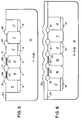
- Figure 5 is a simplified diagrammatic elevation view of the 6.0 mask field oxidation step showing the framing field oxide regions for the CMOS transistor structure and for the resistor structure.
- Figure 6 is a simplified diagrammatic elevation view of the 7.0 poly mask blanket deposition step showing the deposited polycrystalline silicon layer over the CMOS transistor structure NWell and PWell and over the resistor PWell.
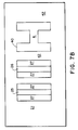
- Figure 7A is a simplified diagrammatic elevation view of the 8.0 mask and etch step showing the new 8.0 gate definition mask with LDD definition openings for the CMOS transistor structure and also functioning as a resistor structure definition mask with a resistor structure definition opening for the new resistor structure.
- Figure 7B is a simplified fragmentary diagrammatic plan view of the new 8.0 gate definition mask of Figure 7A.
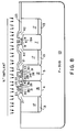
- Figure 8 is a simplified diagrammatic elevation view of the 8.0 mask, etch and implant step showing the implantation of N type atoms through the LDD definition openings of the new 8.0 gate definition mask and also showing the implantation of the same N type atoms through the resistor structure definition openings of the new 8.0 gate definition mask.
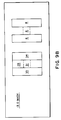
- Figure 9A is a simplified diagrammatic elevation view of the 13.0 mask, etch and implant step showing the new 13.0 NMOS source/drain definition mask with source/drain definition openings for the NMOS transistor structure and also functioning as a resistor contacts definition mask with a resistor contacts region definition opening for the resistor structure.
- Figure 9B is a simplified fragmentary diagrammatic plan view of the 13.0 mask, etch and implant step showing the new 13.0 NMOS source/drain definition mask of Figure 9A.
- Figure 10 is a simplified diagrammatic elevation view of the 14.0 contact definition mask, etch and deposition step showing the new Metal 1 definition mask with Metal 1 deposition definition openings and also functioning as a resistor Metal 1 contacts definition mask with a resistor Metal 1 definition opening for the resistor structure, using a low temperature oxide as the Metal 1 definition mask.
- FIG. 1 A new MOS transistor and resistor structure 1 according to the present invention is illustrated in FIG. 1.
- Said transistor and resistor structure 1 includes a new resistor structure 2 that may be coupled either to an input or an output of an advanced CMOS transistor structure 3 , wherein said CMOS transistor structure 3 is a complementary pair of transistors, including a PMOS transistor 4 and an NMOS transistor 5 .
- a shallow, self-aligned and highly-defined resistive region 6 of said resistor structure 2 is formed of N type atoms, preferably Phosphorus, with a sheet resistance of about 1600 ohms/sq.
- Said resistor structure 2 includes a resistive region 6 , a retrograde resistor PWell region 7 and resistor contact regions 8 .
- the sheet resistance of said resistor structure 2 exceeds that of similar prior art resistors by 2 to 3 times because the concentration of said N type atoms used to form said resistive region 6 is only about one-third of the concentration generally used.
- the fabrication process used to form said resistor structure 2 has been integrated into the CMOS fabrication steps of a new BICMOS fabrication process without adding any new steps.
- the new CMOS fabrication process is hereafter described and those steps related to the fabrication of said resistor structure 2 are illustrated in FIGS. 2-10.
- the new CMOS mask structures are also shown in these figures.
- the overall CMOS transistor structure mask sequence can be summarized as follows: Mask No.
- an initial oxide layer 9 is grown from a substrate 10 of P type semiconductor material to a depth of about 4000 ⁇ .
- An oxide photoresist layer is then deposited on said initial oxide layer 9 to form the 2.0 mask (not shown).
- the 2.0 mask, etch and implant sequence is used to form a retro NWell region 16 .
- the 3.0 mask, etch and implant sequence is used to define and implant a retro PWell region 12 of said CMOS transistor structure 3 and channel stop regions 13 that are adjacent to other active structures (not shown).
- the 3.0 mask is modified to include a resistor PWell definition opening 50 for implanting said resistor retro PWell region 7 .
- Boron atoms are implanted to a P+ concentration in said retro PWell region 12 , said channel stop regions 13 and said resistor retro PWell region 7 .
- the Boron implantation is preferably achieved at 1.15x10¹⁴ ions/cm2 @ 120 Kev.
- a single crystal epitaxial layer 15 of N ⁇ silicon is then deposited uniformly over a first integrated circuit structure surface 14 in a blanket epitaxial deposition. In the thermal cycle of the formation of said epitaxial layer 15 said retro NWell region 16 , said retro PWell region 12 , and said resistor PWell region 7 up-diffuse to some extent, as illustrated in FIG. 3.
- Isolation oxide regions 17 are established around said CMOS transistor structure 3 and said resistor structure 2 using the 4.0 mask, etch and oxidation growth sequence. Said isolation oxide regions 17 diffuse to meet said channel stop regions 13 , pinching any potential channel in that location. The oxidation process further causes upward diffusion of said retro NWell 16 , said retro PWell 12 , and said resistor PWell 7 .
- the 5.0 mask is used to implant said isolation oxide regions 17 with an N+ concentration of phosphorus atoms as a gettering agent.
- a uniform nitride layer 18 is deposited in a blanket chemical vapor deposition across a second integrated circuit structure surface 14a , wherein a thin epitaxial layer 15a is also formed.
- the 6.0 active mask is formed for etching said nitride layer 18 and defining active regions 19 of said CMOS transistor structure 3 and said resistor structure 2 .
- Openings 20 in the 6.0 mask define first field oxide regions 21 for framing said CMOS transistor structure 3 and said resistor structure 2 during subsequent oxidation steps.
- said field oxide regions 21 which add about 1000 ⁇ to the thickness of said isolation oxide regions 17 , isolate said PMOS transistor 4 from said NMOS transistor 5 .
- a second field oxide region 42 isolates said CMOS transistor structure 3 from said resistor structure 2 , forming a second frame about said resistor structure 2 .
- said nitride layer 18 is stripped from all surfaces and CMOS transistor active regions 19a are opened to expose said epitaxial oxide layer 15a .
- Said epitaxial oxide layer 15a is consumed in an oxidation step to form a thin gate oxide layer 22 in said transistor active regions 19a .
- a blanket layer of polycrystalline silicon (poly) 23 is then chemically vapor-deposited over a CMOS transistor/resistor surface 24 to a depth of about 3500 ⁇ , with doping as necessary to adjust the threshold voltage for said CMOS transistor structure 3 .
- the 8.0 poly gate definition mask and etch steps define an NWell poly gate 25 and a PWell poly gate 26 of said CMOS transistor structure 3 , located between said first field oxide regions 21 .
- the 8.0 poly gate definition mask steps define both poly gates 25 and 26 using a photoresist layer and photolithographic stepper followed by etching said poly layer 23 and leaving behind said poly gates 25 and 26 over said gate oxide layer 22 of said CMOS transistor structure 3 .
- the 8.0 gate definition mask is designed to tightly control the dimensions of low density drain (LDD) definition openings 27 between said first field oxide regions 21 . It also provides for self-alignment of said poly gates 25 and 26 .
- LDD low density drain
- the 8.0 mask is modified to include a resistor region opening 53 for implanting said resistive region 6 , and for etching said gate oxide layer 22 formed on the surface of said resistor PWell 7 .
- Said resistor region opening 53 forms a highly-defined poly frame 40 , setting the dimensions of said resistive region 6 and said resistor contacts 8 of said resistor PWell region 7 .
- Said resistor region opening 53 is completely open, providing no gate for said resistor PWell 7 .
- a gate seal oxide layer 28 is grown over said gate oxide layer 22 and said poly gates 25 and 26 , wherein said gate seal oxide layer 28 acts as a standoff, or spacer, for transistor channels 29 underlying said poly gates 25 and 26 .
- Said gate oxide seal layer 28 is preferably grown to a thickness of about 400 ⁇ over said poly gates 25 and 26 , at a temperature of about 900°C, in order to provide highly-defined gates that have length dimensions, L, of about 2.0 microns. This corresponds to effective channel lengths L eff in the range from 0.5 to 0.8 micron.
- Said resistor region opening 53 provides said resistive region 6 with the same dimensions as said transistor channels 29 and the 8.0 mask is used to mask said resistive region 6 to prevent the formation of said gate seal oxide layer 28 in that region.
- the 8.0 poly gate definition mask, etch and implant sequence is also used to define and implant low density drain (LDD) regions 30 in said LDD definition openings 27 , wherein said LDD regions 30 are used to reduce hot electron effects.
- said first field oxide regions 21 and said poly gates 25 and 26 with gate oxide seal layer 28 define the location of said LDD regions 30 .
- Relatively fast-diffusing Phosphorus atoms are implanted to an N ⁇ concentration in those sections of said transistor active regions 19a not masked by said poly gates 25 and 26 .
- the LDD Phosphorus implantation is preferably conducted at a level of 1.3x10¹³ ions/cm2 @ 60 Kev.
- This implantation is conducted at two angles, an angle of about +7° from the perpendicular to the plane of the surface of said CMOS transistor structure 3 , and an angle of about -7° from the same perpendicular.
- the implantation of said LDD 30 through said gate oxide layer 22 and into said epitaxial layer 15 is done at an angle and at double dose in order to negate the shadowing effects caused by sealed poly gates 25 and 26 .
- a portion of said transistor active regions 19a are lightly doped, thereby providing a gradual transition from poly gate source regions 33 and 35 , through gate channel regions 31 and into drain regions 34 and 36 so as to further reduce hot electron effects.
- the LDD Phosphorus is also implanted through said resistor region opening 53 of the modified 8.0 mask, thereby shallowly doping a resistor active region 19b of said resistor PWell 7 to form said resistive region 6 and initially defining said resistor contacts 8 .
- Subsequent annealing at about 1000°C drives the low dose phosphorus implant to a depth of about 1500-2000 ⁇ into said epitaxial layer 15 in said active regions 19a and 19b .
- this drive is relatively deep, it still provides a resistor that is much shallower than prior art resistors.
- the sheet resistance of said resistor region 6 is much higher than prior art structures because said LDD regions 30 are doped at a concentration about one-third less than prior art LDD implants.
- the tightly-controlled 8.0 mask is utilized, along with very low doping levels, to form said resistive region 6 with a sheet resistance that is not only highly-defined, but that is also highly-resistant.
- the 12.0 mask, etch, and implant sequence is used to define a P+ PMOS source region 35 and a P+ PMOS drain region 36 of said PMOS transistor 4 .
- Boron Difluoride (BF2) molecules are implanted through the 12.0 mask at a concentration of 3.0x10¹⁵ ions/cm2 @ 65 Kev.
- the 13.0 mask, etch and implant sequence is used to define and implant N+ NMOS source region 33 and N+ NMOS drain region 34 of said NMOS transistor 5 .
- Arsenic atoms are implanted through the 13.0 mask at a concentration of 7.0x10¹⁵ ions/cm2 @ 100 Kev.
- the 13.0 mask is modified to include resistor contacts openings 54 for implanting said resistor contacts 8 .
- Said resistor contacts openings 54 provide said resistor contacts with the same dimensions as said NMOS source region 33 and said NMOS drain region 34 , both of which are well-defined.
- Said resistor contacts 8 utilizing the same implantation step involved in the formation of said NMOS source region 33 and said NMOS drain region 34 .
- a blanket low-temperature oxide layer (LTO) 39 is blanket-deposited over said CMOS transistor/resistor surface 24 , including said poly frame 40 .
- the 14.0 CMOS contact definition mask and etch sequence removes said LTO 39 over CMOS metal contact areas 41 corresponding to said source regions 33 and 35 and said drain regions 34 and 36 .
- the 14.0 mask is modified to include a resistor contacts formation region 55 in preparation of the Metal 1 deposition.
- said CMOS metal contact areas 41 and said resistor contacts formation region 55 are formed by a Platinum deposition step.
- a first metal layer 43 is deposited using the Metal 1 mask and deposition sequence followed by deposition of a second metal layer using the 17.0 Metal 2 mask and deposition sequence.
- the 15.0 Metal 1 deposition mask is modified to include a resistor Metal 1 definition opening 57 for depositing resistor Metal 1 contacts 58 .
Landscapes
- Metal-Oxide And Bipolar Metal-Oxide Semiconductor Integrated Circuits (AREA)
- Semiconductor Integrated Circuits (AREA)
Applications Claiming Priority (2)
| Application Number | Priority Date | Filing Date | Title |
|---|---|---|---|
| US802878 | 1985-11-29 | ||
| US80287891A | 1991-12-06 | 1991-12-06 |
Publications (1)
| Publication Number | Publication Date |
|---|---|
| EP0545363A1 true EP0545363A1 (fr) | 1993-06-09 |
Family
ID=25184967
Family Applications (1)
| Application Number | Title | Priority Date | Filing Date |
|---|---|---|---|
| EP92120493A Withdrawn EP0545363A1 (fr) | 1991-12-06 | 1992-12-01 | Procédé de fabrication d'un circuit intégré et structure |
Country Status (3)
| Country | Link |
|---|---|
| EP (1) | EP0545363A1 (fr) |
| JP (1) | JPH05291517A (fr) |
| KR (1) | KR930014958A (fr) |
Cited By (9)
| Publication number | Priority date | Publication date | Assignee | Title |
|---|---|---|---|---|
| EP0880165A1 (fr) * | 1997-05-20 | 1998-11-25 | STMicroelectronics S.r.l. | Procédé de fabrication d'un circuit intégré avec des transistors MOS ayant de hauts voltages de claquage et avec des résistances de précision |
| EP0975021A1 (fr) * | 1998-07-22 | 2000-01-26 | STMicroelectronics S.r.l. | Procédé de fabrication d'un dispositif électronique comprenant des transistors de type MOS avec jonctions salicidées et résistors non-salicidées |
| US6348370B1 (en) * | 1999-07-27 | 2002-02-19 | Texas Instruments Incorporated | Method to fabricate a self aligned source resistor in embedded flash memory applications |
| US6725159B2 (en) | 1996-09-06 | 2004-04-20 | Snaptrack Incorporated | GPS receiver and method for processing GPS signals |
| US7005712B2 (en) * | 2003-01-17 | 2006-02-28 | Seiko Epson Corporation | Method for manufacturing a semiconductor device |
| US7982222B2 (en) | 1999-06-23 | 2011-07-19 | Semiconductor Energy Laboratory Co., Ltd. | EL display device and electronic device |
| CN102403272A (zh) * | 2010-09-08 | 2012-04-04 | 北大方正集团有限公司 | 高压互补金属氧化物半导体的制备方法 |
| EP2317541A3 (fr) * | 2009-10-22 | 2014-05-07 | Sanyo Electric Co., Ltd. | Procédé de fabrication d'un dispositif semi-conducteur |
| CN114023702A (zh) * | 2022-01-06 | 2022-02-08 | 南京华瑞微集成电路有限公司 | 一种解决电阻非线性的智能功率mos管的制造方法 |
Families Citing this family (1)
| Publication number | Priority date | Publication date | Assignee | Title |
|---|---|---|---|---|
| KR100482359B1 (ko) * | 1997-07-11 | 2006-05-11 | 삼성전자주식회사 | 반도체소자및그제조방법 |
Citations (3)
| Publication number | Priority date | Publication date | Assignee | Title |
|---|---|---|---|---|
| US4830976A (en) * | 1984-10-01 | 1989-05-16 | American Telephone And Telegraph Company, At&T Bell Laboratories | Integrated circuit resistor |
| EP0320217A2 (fr) * | 1987-12-07 | 1989-06-14 | Texas Instruments Incorporated | Procédé pour fabriquer un transistor du type twin-well-BICMOS |
| EP0455376A2 (fr) * | 1990-04-27 | 1991-11-06 | Digital Equipment Corporation | Méthode de fabrication d'un circuit intégré comportant une résistance de haute précision |
-
1992
- 1992-12-01 EP EP92120493A patent/EP0545363A1/fr not_active Withdrawn
- 1992-12-03 KR KR1019920023177A patent/KR930014958A/ko not_active Withdrawn
- 1992-12-04 JP JP4350167A patent/JPH05291517A/ja active Pending
Patent Citations (3)
| Publication number | Priority date | Publication date | Assignee | Title |
|---|---|---|---|---|
| US4830976A (en) * | 1984-10-01 | 1989-05-16 | American Telephone And Telegraph Company, At&T Bell Laboratories | Integrated circuit resistor |
| EP0320217A2 (fr) * | 1987-12-07 | 1989-06-14 | Texas Instruments Incorporated | Procédé pour fabriquer un transistor du type twin-well-BICMOS |
| EP0455376A2 (fr) * | 1990-04-27 | 1991-11-06 | Digital Equipment Corporation | Méthode de fabrication d'un circuit intégré comportant une résistance de haute précision |
Non-Patent Citations (2)
| Title |
|---|
| PATENT ABSTRACTS OF JAPAN vol. 014, no. 145 (E-905)19 March 1990 & JP-A-20 09 162 ( TOSHIBA CORP. ) 12 January 1990 * |
| PATENT ABSTRACTS OF JAPAN vol. 10, no. 42 (E-382)(2099) 19 February 1986 & JP-A-60 198 853 ( NIPPON DENKI K.K. ) 8 October 1985 * |
Cited By (13)
| Publication number | Priority date | Publication date | Assignee | Title |
|---|---|---|---|---|
| US6725159B2 (en) | 1996-09-06 | 2004-04-20 | Snaptrack Incorporated | GPS receiver and method for processing GPS signals |
| US6027965A (en) * | 1997-05-20 | 2000-02-22 | Stmicroelectronics S.R.L. | Method of manufacturing an integrated circuit with MOS transistors having high breakdown voltages, and with precision resistors |
| EP0880165A1 (fr) * | 1997-05-20 | 1998-11-25 | STMicroelectronics S.r.l. | Procédé de fabrication d'un circuit intégré avec des transistors MOS ayant de hauts voltages de claquage et avec des résistances de précision |
| EP0975021A1 (fr) * | 1998-07-22 | 2000-01-26 | STMicroelectronics S.r.l. | Procédé de fabrication d'un dispositif électronique comprenant des transistors de type MOS avec jonctions salicidées et résistors non-salicidées |
| US6300181B1 (en) | 1998-07-22 | 2001-10-09 | Stmicroelectronics S.R.L. | Process for manufacturing an electronic device including MOS transistors with salicided junctions and non-salicided resistors |
| US7982222B2 (en) | 1999-06-23 | 2011-07-19 | Semiconductor Energy Laboratory Co., Ltd. | EL display device and electronic device |
| US6348370B1 (en) * | 1999-07-27 | 2002-02-19 | Texas Instruments Incorporated | Method to fabricate a self aligned source resistor in embedded flash memory applications |
| US7005712B2 (en) * | 2003-01-17 | 2006-02-28 | Seiko Epson Corporation | Method for manufacturing a semiconductor device |
| EP2317541A3 (fr) * | 2009-10-22 | 2014-05-07 | Sanyo Electric Co., Ltd. | Procédé de fabrication d'un dispositif semi-conducteur |
| CN102403272A (zh) * | 2010-09-08 | 2012-04-04 | 北大方正集团有限公司 | 高压互补金属氧化物半导体的制备方法 |
| CN102403272B (zh) * | 2010-09-08 | 2013-10-16 | 北大方正集团有限公司 | 高压互补金属氧化物半导体的制备方法 |
| CN114023702A (zh) * | 2022-01-06 | 2022-02-08 | 南京华瑞微集成电路有限公司 | 一种解决电阻非线性的智能功率mos管的制造方法 |
| CN114023702B (zh) * | 2022-01-06 | 2022-03-25 | 南京华瑞微集成电路有限公司 | 一种解决电阻非线性的智能功率mos管的制造方法 |
Also Published As
| Publication number | Publication date |
|---|---|
| JPH05291517A (ja) | 1993-11-05 |
| KR930014958A (ko) | 1993-07-23 |
Similar Documents
| Publication | Publication Date | Title |
|---|---|---|
| US5169794A (en) | Method of fabrication of pnp structure in a common substrate containing npn or MOS structures | |
| US5424572A (en) | Spacer formation in a semiconductor structure | |
| KR930008018B1 (ko) | 바이씨모스장치 및 그 제조방법 | |
| US4788160A (en) | Process for formation of shallow silicided junctions | |
| US5338696A (en) | Method of fabricating BiCMOS device | |
| JP3205361B2 (ja) | 縦方向電流によるパワーmosトランジスタを製造するための方法 | |
| US5079182A (en) | Bicmos device having self-aligned well tap and method of fabrication | |
| US5439831A (en) | Low junction leakage MOSFETs | |
| EP0994510B1 (fr) | Procédé de fabrication d'une structure LDD pour un circuit de protection contre les décharges (ESD) | |
| JPH06326306A (ja) | Mosトランジスタおよびその製造方法 | |
| EP0450375B1 (fr) | Interconnexion et procédé de fabrication pour des dispositifs à semi-conducteurs | |
| US5231042A (en) | Formation of silicide contacts using a sidewall oxide process | |
| US5389553A (en) | Methods for fabrication of transistors | |
| US6576521B1 (en) | Method of forming semiconductor device with LDD structure | |
| JPH05291517A (ja) | 高精度高抵抗の抵抗体構造とその製造方法 | |
| EP0595484A1 (fr) | Procédé IC de type NMOS LDD PMOS HALO pour des transistors CMOS | |
| KR100281397B1 (ko) | 초박형 soi 정전기방전 보호 소자의 형성 방법 | |
| JP3165715B2 (ja) | 半導体装置の製造方法 | |
| JPH0837239A (ja) | 半導体装置および半導体装置の製造方法 | |
| JP3097095B2 (ja) | 半導体装置の製造方法 | |
| EP0224712A2 (fr) | Dispositif intégré comprenant des transistors du type bipolaire et du type complémentaire métal-oxyde semi-conducteur | |
| JPS63302562A (ja) | Mos型半導体装置の製造方法 | |
| JPH0964361A (ja) | 半導体装置の製造方法 | |
| JPS61139057A (ja) | 半導体集積回路装置の製造方法 | |
| JPH02231729A (ja) | 半導体装置の製造方法 |
Legal Events
| Date | Code | Title | Description |
|---|---|---|---|
| PUAI | Public reference made under article 153(3) epc to a published international application that has entered the european phase |
Free format text: ORIGINAL CODE: 0009012 |
|
| AK | Designated contracting states |
Kind code of ref document: A1 Designated state(s): DE FR GB NL |
|
| 17P | Request for examination filed |
Effective date: 19931123 |
|
| STAA | Information on the status of an ep patent application or granted ep patent |
Free format text: STATUS: THE APPLICATION IS DEEMED TO BE WITHDRAWN |
|
| 18D | Application deemed to be withdrawn |
Effective date: 19960702 |