EP0546658B1 - Procédé et dispositif pour le contrÔle dans un émetteur haute-fréquence, des interférences spectrales haute-fréquences dans des canaux adjacents - Google Patents
Procédé et dispositif pour le contrÔle dans un émetteur haute-fréquence, des interférences spectrales haute-fréquences dans des canaux adjacents Download PDFInfo
- Publication number
- EP0546658B1 EP0546658B1 EP92307735A EP92307735A EP0546658B1 EP 0546658 B1 EP0546658 B1 EP 0546658B1 EP 92307735 A EP92307735 A EP 92307735A EP 92307735 A EP92307735 A EP 92307735A EP 0546658 B1 EP0546658 B1 EP 0546658B1
- Authority
- EP
- European Patent Office
- Prior art keywords
- amplifier
- signal
- circuit
- output
- pin diode
- Prior art date
- Legal status (The legal status is an assumption and is not a legal conclusion. Google has not performed a legal analysis and makes no representation as to the accuracy of the status listed.)
- Expired - Lifetime
Links
Images
Classifications
-
- H—ELECTRICITY
- H03—ELECTRONIC CIRCUITRY
- H03G—CONTROL OF AMPLIFICATION
- H03G3/00—Gain control in amplifiers or frequency changers
- H03G3/20—Automatic control
- H03G3/30—Automatic control in amplifiers having semiconductor devices
- H03G3/3036—Automatic control in amplifiers having semiconductor devices in high-frequency amplifiers or in frequency-changers
- H03G3/3042—Automatic control in amplifiers having semiconductor devices in high-frequency amplifiers or in frequency-changers in modulators, frequency-changers, transmitters or power amplifiers
Definitions
- the present invention relates to radio frequency (RF) amplifiers and more particularly to a method and apparatus for controlling RF spectrum splatter transients during initial activation of an RF transmitter.
- RF radio frequency
- Class A, B, and AB amplifiers are inefficient compared to Class C amplifiers. Because of their efficiency, Class C amplifiers are often used in radio transmitters. By definition, a Class C amplifier is biased so that its quiescent state is "off". Upon receiving an input RF signal, the Class C amplifier generates a somewhat distorted, amplified RF output signal, and a tank circuit tuned to the desired output frequency effectively re-shapes the amplified RF signal.
- Class C amplifiers can have extremely fast self-activation or "turn-on" times. Once the amplifier receives an input RF signal, the rise time of the output RF signal envelope can be extremely fast. The rise time is defined for purposes of the present invention as the time period it takes for a transmitted RF signal to increase from essentially zero power to full transmitter power.
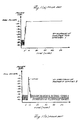
- a graph of radio transmitter power in decibels (dB) versus time (msec) is shown in FIGURE 1A. For purposes of illustration, only the envelope of the output RF signal is shown. The transmitter is turned “on” at approximately the 5 millisecond mark on the illustrated time scale, and the transmitted signal increases from an average quiescent noise level of -80 dB to full RF carrier power, characterized as zero dB, in a few microseconds. In fact, the rise time of the Class C amplifier signal response is so fast that the RF envelope is nearly a step function.
- the presence of RF energy outside of an assigned frequency band may spill over into adjacent channels and cause interference with other signal transmissions.
- different transmitters may be assigned to specific channels corresponding to particular frequency bands in the RF spectrum. Excessively abrupt activation of a transmitter assigned to one channel (having a preset bandwidth) may cause transient splatter in the RE spectrum and be detected as transient noise in adjacent channels. In fact, such transmitter turn-on noise may interfere with several (e.g. five or more) adjacent and nearby channels.
- FIGURE 1A An example RF envelope of a radio transmitter using channel 1 is shown in FIGURE 1A.
- the effect on an adjacent channel 2 of turning on that transmitter is illustrated in FIGURE 1B.
- a sharp noise spike occurs in the adjacent channel 2.
- This noise spike is only 5 dB below full power and may even trip the squelch circuits of sensitive receivers tuned to channel 2.
- such a noise spike may cause significant errors in information then being transmitted over channel 2, especially if the information is digital data.
- listeners may experience such cross-channel noise spikes as loud clicks or pops on the channel.
- each transceiver may be activated many times over a short time interval. In other words, every time a user wishes to talk, that user activates his transmitter causing interference to one or more adjacent channels.
- Prior art transmitter designers have recognized the need to control amplifier gain.
- prior art amplifiers fail in some cases to sufficiently suppress interchannel noise caused by transmitter turn-on transients. This is especially so at higher carrier frequencies with closely spaced channels.
- French Patent Application No. FR-A-2566206 discloses a transmitter having an arrangement for limiting the output power radiated from a transmitter and to prevent overshoots.
- EP-A-0156398 discloses a burst signal generating apparatus which requires an externally generated waveform to modify the slopes of the carrier waves.
- the present invention is concerned with providing a simple and effective mechanism for reducing such transient noise caused by radio transmitter activations.
- RF snubber circuit in parallel with the transmitter output, RF envelope rise time may be slowed considerably. As a result, adjacent channel interference is substantially eliminated.
- an amplifier circuit as set out in claim 1.
- an RF envelope detector is used in conjunction with an RC circuit to self-generate a transient control circuit during abrupt envelope increases.
- the transient control circuit automatically and temporarily functions as an RF attenuator to slow the actual envelope rise time.
- Suitable static discharge resistance may also be used to reset automatically the circuit for use at the next transmitter activation.
- An exemplary RF snubber circuit takes advantage of the operational characteristics of a PIN diode at radio frequencies.
- the PIN diode functions as a half wave rectifier to generate a DC current which is accumulated on a small first series-connected capacitor.
- the PIN diode and capacitor act as an envelope detector.
- the envelope detector automatically powers an RC time delay circuit.
- DC current flows through an RC circuit (a series connected resistor and a second capacitor) shunt-connected across the first capacitor to result in a sustained yet transient biasing current for the PIN diode.
- the first capacitor acts as an RF bypass for the RF signal, and thus, effectively connects the PIN diode directly across the RF amplifier output.
- the shunt PIN diode resistance loads the amplifier output and temporarily attenuates it.
- the second capacitor through which the biasing current flows is, in this exemplary embodiment, large relative to the value of the first (RF bypass/charging capacitor) that couples the diode to ground. Consequently, the second capacitor maintains a diode bias current for a significant time interval, and in the process, slows the rise time of the RF envelope across the now resistive PIN diode.
- the first capacitor acts to keep the PIN diode effectively connected in shunt across the RF output while the RC time constant of the biasing current through second capacitor keeps the PIN diode resistive. Consequently, the rise time or turn-on characteristic of the RF envelope is reduced or slowed sufficiently to prevent spurious transient turn-on interference in adjacent channels.
- the PIN diode of the present invention does not require an externally controlled bias current in order to achieve the desired resistive characteristic at transistor turn-on time.
- the bias current is self-adjusting using simple, passive circuit components. Once the transmitter RF envelope has reached a steady or constant power level, the capacitors reach a steady state dc voltage and the PIN diode bias current automatically disappears -- thus removing undesirable RF loading and attenuation during ongoing transmitter operation. No external voltage source or control mechanism is required to actively bias the PIN diode; no external device or signal is required to remove the biasing current.
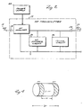
- RF amplifier 16 of RF transmitter 10 receives an RF input signal 12 through a dc blocking and RF coupling capacitor 14.
- the RF amplifier 16 is characteristically a Class C amplifier which is biased to cutoff until it receives RF input signal 12.
- a dc power supply 26 provides the necessary dc operating power.
- RF amplifier 16 When RF amplifier 16 receives an RF input signal 12, it self-activates or turns “on”. It also automatically activates an RF snubber circuit 34 shunt connected across the amplifier output to slow the effective turn-on time of the amplifier output signal -- thus preventing transient RF spectral noise on adjacent frequency channels.
- An exemplary RF snubber circuit 34 will be described in considerably more detail below.
- the amplified output signal from the RF amplifier 16 drives a conventional tuned tank circuit 46 which provides the RF output signal 54 through RF coupling capacitor 52.
- RF input signal 12 is received by RF amplifier circuit 16 through RF coupling capacitor 14.
- the RF amplifier 16 includes bipolar junction transistor 18. Connected to the base of transistor 18 is the usual base-emitter resistor 20. Connected to the emitter of transistor 18 are the usual bias resistor 22 (to determine the slope of the amplifier operating line) and RF bypass capacitor 24.
- the conventional power supply 26 includes a dc voltage supply 28 connected to the collector terminal of transistor 18 through the usual radio frequency "choke" inductor 30.
- the voltage supply 28 is also shunted by an RF bypass capacitor 32 which isolates the dc power supply 28 from the RF signal.
- RF snubber circuit 34 The RF output of RF amplifier 16 is connected to RF snubber circuit 34 through RF coupling capacitor 33.
- RF snubber circuit 34 includes PIN diode 36 connected in series with an RF bypass charging capacitor 40 to ground. Across the RF bypass charging capacitor 40, an RC time delay bias circuit is connected including resistor 38 and capacitor 42. Static discharge resistor 44 is also provided to insure bleed off of residual capacitor charges when the transmitter is turned off -- thus automatically resetting RF snubber 34 for another cycle of operation when the transmitter is again activated.
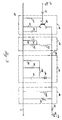
- PIN diode 36 The operation of PIN diode 36 will now be described in further detail with regard to FIGURE 4.
- the basic structure of the PIN diode consists of a high resistivity intrinsic region (I region) bounded by highly acceptor-doped (P +) and donor-doped (N+) regions, both of which have high conductivity. With no bias current applied, or if a reverse bias voltage is applied, the diode functions as a capacitor.
- a PIN diode may be viewed as a capacitor (when at zero or reverse bias) with an electronically variable resistance (when forward biased) whose resistance value may be controlled by varying its forward bias current.
- PIN diodes are used in radio frequency environments as attenuators -- even to control the gain of RF amplifiers.
- the prior art typically requires an external source of controlled dc bias current to control the PIN diode.
- the PIN diode 36 does not require a controlled bias current from an external source. Rather, it will be seen from the following description that the PIN diode 36 as used in the present invention is self-actuated and self-adjusting.
- the transient dc current flowing through capacitor 42, resistor 38 and PIN diode 36 functions as a dc biasing current for the PIN diode. With that forward biasing current, the PIN diode 36 temporarily acts as a loading resistor attenuating the RF output signal. However, when a steady state RF envelope amplitude is reached, the biasing current becomes zero. Accordingly, the PIN diode 36 no longer functions as a resistive load.
- the RF snubber circuit 34 is thus effectively open circuited and can be considered either removed from the transmission circuit 10 or as a relatively constant capacitance which can become part of the tank circuit.
- the RF snubber circuit 34 is self-actuating; no external source of voltage is required to generate the requisite transient dc biasing current for the PIN diode 36.
- the biasing current is applied to the PIN diode 36 simultaneously with transmitter activation. It is the changing (increasing) rectified RF signal envelope that makes the snubber circuit 34 self-actuating.
- the snubber circuit 34 is self-regulating for two reasons. First, the faster the rise time of the RF envelope, the greater the transient bias current pulled through the RF snubber circuit 34.
- the RF snubber functions temporarily like a resistor in parallel with the tuning circuit 46 to attenuate the RF envelope during turn-on. Second, when the transmitter has reached full power, the RF snubber circuit capacitors 40 and 42 effectively remove the snubber circuit.
- the RC time constant of the biasing current through the resistor 38 and capacitor 42 control the resultant rise time and shape of the RF envelope.
- the value of the capacitor 42 is in this embodiment much greater than that of the capacitor 40 and it effectively resists too rapid an increase in its voltage.
- a further feature of the present invention is the connection of a very large static discharge bleeder resistor 44, e.g., 10 megaohms, in parallel with capacitor 42.
- Resistor 44 has two functions. First, it is sufficiently large so as to not materially affect the voltage across the resistor 44, capacitor 42, and capacitor 40 during circuit operation. Second, it is sufficiently small to discharge capacitors 40 and 42 within a reasonable time of stored charge when the transmitter 10 is turned off. As a result, the RF snubber circuit will be immediately preset to operational readiness for use the next time transmitter 10 is activated.
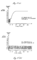
- FIGURES 5A and 5B The RF turn-on envelope in channel 1 and the related RF spectrum in an adjacent channel 2 for an RF transmitter incorporating the beneficial effects of the present invention are shown in FIGURES 5A and 5B.
- FIGURE 5A shows that when the transmitter 10 is activated, the rise time to full power for the RF envelope is slowed down considerably.
- the slope of the turn-on curve has been decreased so that RF power is increased to full power in a more gradual, controlled manner.
- the shape of the curve has been modified so that it "rolls over" smoothly rather than making a sharp, square wave like transition.
- FIGURE 5B the RF spectrum in an adjacent channel 2 is no longer affected by the turning on of a transmitter on channel 1. Voltage spikes or transients in adjacent channels are substantially eliminated.
- RF bypass capacitor 40 is 100 picofarads
- resistor 38 is 47 kilohms
- capacitor 42 is 0.047 microfarads
- static bleeder resistor 44 is 10 megohms.
Landscapes
- Transmitters (AREA)
- Amplifiers (AREA)
- Tone Control, Compression And Expansion, Limiting Amplitude (AREA)
Claims (13)
- Un circuit amplificateur pour utilisation dans un émetteur RF pour amplifier un signal RF d'entrée, le circuit amplificateur comprenant :caractérisé par un circuit de contrôle et de commande (34) qui répond à une variation rapide de l'enveloppe du signal de sortie de l'amplificateur en augmentant la charge efficace appliquée à l'amplificateur, ledit circuit de contrôle et de commande comprenant un atténuateur RF auto-régulateur (34) relié en parallèle avec la sortie de l'amplificateur pour maítriser la vitesse de variation de la réponse de sortie de l'amplificateur suite à la réception initiale d'un signal RF d'entrée.un amplificateur (16) qui reçoit le signal RF d'entrée à un premier niveau de puissance et qui produit un signal RF de sortie à un deuxième niveau de puissance plus élevé ; et
- Un circuit selon la revendication 1, dans lequel l'amplificateur (16) est un amplificateur de classe C.
- Un circuit selon la revendication 1 ou la revendication 2, dans lequel l'atténuateur RF auto-régulateur est un circuit d'amortissement RF comprenant :un diode PIN (36) reliée à l'une de ses extrémités à la sortie de l'amplificateur etun circuit RC (38, 42) qui génère un courant de polarisation en courant continu transitoire pour la diode PIN, pour régler la vitesse de variation de la réponse de l'amplificateur.
- Un circuit selon la revendication 3. dans lequel la constante de temps du courant de polarisation transitoire est importante par rapport à la constante de temps, autrement attendue, de la réponse de l'amplificateur.
- Un circuit selon la revendication 3 ou la revendication 4, dans lequel le circuit RC comprend une résistance reliée en série et un premier condensateur relié à l'autre extrémité de la diode PIN, et un deuxième condensateur (40) relié à l'autre extrémité de la diode PIN.
- Un circuit selon la revendication 5, dans lequel le circuit d'amortissement RF comprend en outre :une résistance de fuite pour la décharge statique, reliée en parallèle avec le deuxième condensateur.
- Un circuit selon l'une quelconque des revendications précédentes, et comprenant en outre :un circuit LC accordé (46) relié en parallèle avec l'atténuateur RF autorégulateur afin de remettre en forme le signal de sortie RF amplifié de l'amplificateur.
- Un circuit d'un émetteur RF comprenant un amplificateur selon l'une quelconque des revendications précédentes, et dans lequel ledit circuit de contrôle et de commande est adapté sensiblement pour éliminer des interférences sur des fréquences adjacentes provoquées par l'activation de l'amplificateur lors de la présentation initiale d'un signal RF d'entrée.
- Un procédé pour la commande d'un émetteur RF (10) présentant un amplificateur (16) et une dérivation RF avec diode PIN (34), reliée, aux bornes de l'amplificateur, comprenant :la réception d'un signal d'entrée RF à l'entrée d'un amplificateur ; etl'auto-polarisation d'une diode PIN au moyen du signal de sortie de l'amplificateur en réponse à une variation rapide de l'enveloppe du signal de sortie, de sorte que la charge effective de l'amplificateur augmente et de sorte que la vitesse de variation de la réponse de sortie de l'amplificateur soit contrôlée suite à la réception initiale d'un signal RF d'entrée.
- Un procédé selon la revendication 9, dans lequel ladite étape d'auto-polarisation comprend :la génération d'un courant de polarisation à partir du signal de sortie de l'amplificateur RF ;le réglage des variations du courant de polarisation afin de ralentir temporairement la réponse de l'amplificateur au signal RF d'entrée.
- Un procédé selon la revendication 10, comprenant en outre :la génération d'un courant de polarisation d'une diode PIN en réponse à des variations d'un signal RF fourni par l'amplificateur.
- Un procédé selon la revendication 11, dans lequel l'étape de génération comprend la charge d'au moins un condensateur, ledit procédé comprenant en outre :la décharge dudit condensateur lorsque la sortie du signal RF de l'amplificateur diminue.
- Un procédé selon la revendication 11 ou la revendication 12, dans lequel ladite étape de réglage comprend :l'élimination sensible de façon automatique du courant de polarisation de la diode PIN lorsque l'amplificateur arrive à un niveau de sortie RF correspondant à un régime permanent.
Applications Claiming Priority (2)
| Application Number | Priority Date | Filing Date | Title |
|---|---|---|---|
| US07/791,283 US5278519A (en) | 1991-11-13 | 1991-11-13 | Method and apparatus for controlling RF spectral splatter into adjacent channels when activating an RF transmitter |
| US791283 | 1991-11-13 |
Publications (2)
| Publication Number | Publication Date |
|---|---|
| EP0546658A1 EP0546658A1 (fr) | 1993-06-16 |
| EP0546658B1 true EP0546658B1 (fr) | 1998-12-23 |
Family
ID=25153222
Family Applications (1)
| Application Number | Title | Priority Date | Filing Date |
|---|---|---|---|
| EP92307735A Expired - Lifetime EP0546658B1 (fr) | 1991-11-13 | 1992-08-25 | Procédé et dispositif pour le contrÔle dans un émetteur haute-fréquence, des interférences spectrales haute-fréquences dans des canaux adjacents |
Country Status (4)
| Country | Link |
|---|---|
| US (2) | US5278519A (fr) |
| EP (1) | EP0546658B1 (fr) |
| JP (1) | JPH05315880A (fr) |
| DE (1) | DE69227983T2 (fr) |
Families Citing this family (5)
| Publication number | Priority date | Publication date | Assignee | Title |
|---|---|---|---|---|
| GB2278727B (en) * | 1993-06-02 | 1997-04-09 | Nec Corp | Bipolar transistor circuit |
| US6232841B1 (en) * | 1999-07-01 | 2001-05-15 | Rockwell Science Center, Llc | Integrated tunable high efficiency power amplifier |
| US6307429B1 (en) | 2000-01-12 | 2001-10-23 | National Semiconductor Corporation | Extended power ramp table for power amplifier control loop |
| US7634290B2 (en) * | 2005-05-31 | 2009-12-15 | Vixs Systems, Inc. | Adjusting transmit power of a wireless communication device |
| CA2741135C (fr) * | 2007-11-06 | 2015-10-20 | Microoncology Limited | Appareil de sterilisation de plasma produisant des radicaux hydroxyle |
Family Cites Families (18)
| Publication number | Priority date | Publication date | Assignee | Title |
|---|---|---|---|---|
| US3023369A (en) * | 1959-02-09 | 1962-02-27 | Blonder Tongue Elect | Variable-gain transistor circuit |
| US3256381A (en) * | 1962-05-29 | 1966-06-14 | Jack C Cookerly | Tone level control circuit |
| JPS5255359A (en) * | 1975-10-31 | 1977-05-06 | Hitachi Ltd | High-frequency amplifier circuit |
| JPS5340256A (en) * | 1976-09-27 | 1978-04-12 | Alps Electric Co Ltd | Automatic gain controller |
| US4243947A (en) * | 1979-03-28 | 1981-01-06 | General Motors Corporation | Radio frequency amplifier with gain control |
| DE3210452A1 (de) * | 1982-03-22 | 1983-09-29 | Licentia Patent-Verwaltungs-Gmbh, 6000 Frankfurt | Signal-eingangsschaltung |
| US4596043A (en) * | 1982-03-29 | 1986-06-17 | Motorola, Inc. | High efficiency radio frequency signal amplifier for amplifying modulated radio frequency signals in a manner generating minimal splatter |
| US4706262A (en) * | 1984-03-30 | 1987-11-10 | Nec Corporation | FSK or FM burst signal generating apparatus |
| FR2566206B1 (fr) * | 1984-06-18 | 1990-07-13 | Thomson Lgt | Dispositif pour limiter la puissance d'emission d'emetteurs d'ondes radioelectriques |
| US4677392A (en) * | 1985-12-16 | 1987-06-30 | Hughes Aircraft Company | Cascaded internal impedance dependent amplifier with accurate variable gain control |
| US4646036A (en) * | 1985-12-23 | 1987-02-24 | Motorola, Inc. | Signal attenuation circuit |
| US4673886A (en) * | 1986-02-26 | 1987-06-16 | Motorola, Inc. | Adaptively stabilized RF amplifier |
| FI81931C (fi) * | 1989-05-12 | 1990-12-10 | Nokia Mobira Oy | Foerfarande foer alstring av laoga effektnivaoer i saendaren av en radiotelefon. |
| US4924194A (en) * | 1989-05-19 | 1990-05-08 | Motorola, Inc. | RF power amplifier |
| ES2120405T3 (es) * | 1989-06-27 | 1998-11-01 | Nec Corp | Circuito de control de perfil de onda de salida. |
| DE3921102A1 (de) * | 1989-06-28 | 1991-01-10 | Standard Elektrik Lorenz Ag | Sende- und/oder empfangsgeraet |
| US4970479A (en) * | 1989-11-27 | 1990-11-13 | Rockwell International Corporation | Multicoupler including frequency shift filters |
| US5150075A (en) * | 1991-06-03 | 1992-09-22 | Motorola, Inc. | Power amplifier ramp up method and apparatus |
-
1991
- 1991-11-13 US US07/791,283 patent/US5278519A/en not_active Expired - Lifetime
-
1992
- 1992-08-21 JP JP4223086A patent/JPH05315880A/ja not_active Withdrawn
- 1992-08-25 DE DE69227983T patent/DE69227983T2/de not_active Expired - Fee Related
- 1992-08-25 EP EP92307735A patent/EP0546658B1/fr not_active Expired - Lifetime
-
1993
- 1993-08-30 US US08/113,096 patent/US5406227A/en not_active Expired - Lifetime
Also Published As
| Publication number | Publication date |
|---|---|
| EP0546658A1 (fr) | 1993-06-16 |
| JPH05315880A (ja) | 1993-11-26 |
| US5406227A (en) | 1995-04-11 |
| DE69227983T2 (de) | 1999-05-20 |
| US5278519A (en) | 1994-01-11 |
| DE69227983D1 (de) | 1999-02-04 |
Similar Documents
| Publication | Publication Date | Title |
|---|---|---|
| US6026285A (en) | Intermodulation distortion reduction circuit utilizing variable attenuation | |
| US5214393A (en) | Transmission output control circuit | |
| KR100193848B1 (ko) | 대역확산통신기에 있어서 수신신호 이득 자동제어장치 및 방법 | |
| US4528519A (en) | Automatic gain control | |
| US3699457A (en) | Noise blanker circuit including rate bias and rate shutoff circuitry and audio blanking | |
| US3518375A (en) | Voice override circuit | |
| CA2085117C (fr) | Amplificateur de puissance | |
| US4013964A (en) | Automatic gain control means for a single sideband radio receiver | |
| AU734808B2 (en) | Power amplifier and method therein | |
| US5307026A (en) | Variable gain RF amplifier with linear gain control | |
| US5278519A (en) | Method and apparatus for controlling RF spectral splatter into adjacent channels when activating an RF transmitter | |
| US3708756A (en) | Biasing network for transistors | |
| US5381110A (en) | Spurious frequency suppressor | |
| US5568105A (en) | Spurious frequency suppressor | |
| US4147991A (en) | Automatic gain control apparatus | |
| US5565823A (en) | Voltage controlled attenuator using PN diodes | |
| GB2266422A (en) | Attenuators | |
| JP2786323B2 (ja) | 信号減衰回路 | |
| US4660003A (en) | Device for limiting the power transmission of radiowave transmitters | |
| US3430147A (en) | Squelch tail preventing circuit | |
| US1947822A (en) | Automatic tone control | |
| KR100190610B1 (ko) | 자동 이득 제어 회로 | |
| JPH05300029A (ja) | 自動送信電力制御回路の電力増幅器バイアス回路 | |
| KR890001534Y1 (ko) | Tv용 부스터 장치 | |
| US3970949A (en) | High-frequency automatic gain control circuit |
Legal Events
| Date | Code | Title | Description |
|---|---|---|---|
| PUAI | Public reference made under article 153(3) epc to a published international application that has entered the european phase |
Free format text: ORIGINAL CODE: 0009012 |
|
| AK | Designated contracting states |
Kind code of ref document: A1 Designated state(s): DE FR GB IT |
|
| 17P | Request for examination filed |
Effective date: 19931118 |
|
| 17Q | First examination report despatched |
Effective date: 19961008 |
|
| GRAG | Despatch of communication of intention to grant |
Free format text: ORIGINAL CODE: EPIDOS AGRA |
|
| GRAG | Despatch of communication of intention to grant |
Free format text: ORIGINAL CODE: EPIDOS AGRA |
|
| GRAH | Despatch of communication of intention to grant a patent |
Free format text: ORIGINAL CODE: EPIDOS IGRA |
|
| GRAH | Despatch of communication of intention to grant a patent |
Free format text: ORIGINAL CODE: EPIDOS IGRA |
|
| GRAA | (expected) grant |
Free format text: ORIGINAL CODE: 0009210 |
|
| AK | Designated contracting states |
Kind code of ref document: B1 Designated state(s): DE FR GB IT |
|
| REF | Corresponds to: |
Ref document number: 69227983 Country of ref document: DE Date of ref document: 19990204 |
|
| ET | Fr: translation filed | ||
| ITF | It: translation for a ep patent filed | ||
| PG25 | Lapsed in a contracting state [announced via postgrant information from national office to epo] |
Ref country code: GB Free format text: LAPSE BECAUSE OF NON-PAYMENT OF DUE FEES Effective date: 19990825 |
|
| PLBE | No opposition filed within time limit |
Free format text: ORIGINAL CODE: 0009261 |
|
| STAA | Information on the status of an ep patent application or granted ep patent |
Free format text: STATUS: NO OPPOSITION FILED WITHIN TIME LIMIT |
|
| 26N | No opposition filed | ||
| GBPC | Gb: european patent ceased through non-payment of renewal fee |
Effective date: 19990825 |
|
| PG25 | Lapsed in a contracting state [announced via postgrant information from national office to epo] |
Ref country code: FR Free format text: LAPSE BECAUSE OF NON-PAYMENT OF DUE FEES Effective date: 20000428 |
|
| PG25 | Lapsed in a contracting state [announced via postgrant information from national office to epo] |
Ref country code: DE Free format text: LAPSE BECAUSE OF NON-PAYMENT OF DUE FEES Effective date: 20000601 |
|
| REG | Reference to a national code |
Ref country code: FR Ref legal event code: ST |
|
| PG25 | Lapsed in a contracting state [announced via postgrant information from national office to epo] |
Ref country code: IT Free format text: LAPSE BECAUSE OF NON-PAYMENT OF DUE FEES;WARNING: LAPSES OF ITALIAN PATENTS WITH EFFECTIVE DATE BEFORE 2007 MAY HAVE OCCURRED AT ANY TIME BEFORE 2007. THE CORRECT EFFECTIVE DATE MAY BE DIFFERENT FROM THE ONE RECORDED. Effective date: 20050825 |