EP0548968A2 - Optisches Aufzeichnungselement mit einer die Gebrauchsdauer steigernden Schicht - Google Patents
Optisches Aufzeichnungselement mit einer die Gebrauchsdauer steigernden Schicht Download PDFInfo
- Publication number
- EP0548968A2 EP0548968A2 EP92121939A EP92121939A EP0548968A2 EP 0548968 A2 EP0548968 A2 EP 0548968A2 EP 92121939 A EP92121939 A EP 92121939A EP 92121939 A EP92121939 A EP 92121939A EP 0548968 A2 EP0548968 A2 EP 0548968A2
- Authority
- EP
- European Patent Office
- Prior art keywords
- layer
- protective layer
- disk
- support
- protective
- Prior art date
- Legal status (The legal status is an assumption and is not a legal conclusion. Google has not performed a legal analysis and makes no representation as to the accuracy of the status listed.)
- Granted
Links
Images
Classifications
-
- G—PHYSICS
- G11—INFORMATION STORAGE
- G11B—INFORMATION STORAGE BASED ON RELATIVE MOVEMENT BETWEEN RECORD CARRIER AND TRANSDUCER
- G11B7/00—Recording or reproducing by optical means, e.g. recording using a thermal beam of optical radiation by modifying optical properties or the physical structure, reproducing using an optical beam at lower power by sensing optical properties; Record carriers therefor
- G11B7/24—Record carriers characterised by shape, structure or physical properties, or by the selection of the material
- G11B7/2403—Layers; Shape, structure or physical properties thereof
- G11B7/24053—Protective topcoat layers lying opposite to the light entrance side, e.g. layers for preventing electrostatic charging
-
- G—PHYSICS
- G11—INFORMATION STORAGE
- G11B—INFORMATION STORAGE BASED ON RELATIVE MOVEMENT BETWEEN RECORD CARRIER AND TRANSDUCER
- G11B7/00—Recording or reproducing by optical means, e.g. recording using a thermal beam of optical radiation by modifying optical properties or the physical structure, reproducing using an optical beam at lower power by sensing optical properties; Record carriers therefor
- G11B7/24—Record carriers characterised by shape, structure or physical properties, or by the selection of the material
- G11B7/2403—Layers; Shape, structure or physical properties thereof
- G11B7/24067—Combinations of two or more layers with specific interrelation
-
- Y—GENERAL TAGGING OF NEW TECHNOLOGICAL DEVELOPMENTS; GENERAL TAGGING OF CROSS-SECTIONAL TECHNOLOGIES SPANNING OVER SEVERAL SECTIONS OF THE IPC; TECHNICAL SUBJECTS COVERED BY FORMER USPC CROSS-REFERENCE ART COLLECTIONS [XRACs] AND DIGESTS
- Y10—TECHNICAL SUBJECTS COVERED BY FORMER USPC
- Y10S—TECHNICAL SUBJECTS COVERED BY FORMER USPC CROSS-REFERENCE ART COLLECTIONS [XRACs] AND DIGESTS
- Y10S428/00—Stock material or miscellaneous articles
- Y10S428/913—Material designed to be responsive to temperature, light, moisture
-
- Y—GENERAL TAGGING OF NEW TECHNOLOGICAL DEVELOPMENTS; GENERAL TAGGING OF CROSS-SECTIONAL TECHNOLOGIES SPANNING OVER SEVERAL SECTIONS OF THE IPC; TECHNICAL SUBJECTS COVERED BY FORMER USPC CROSS-REFERENCE ART COLLECTIONS [XRACs] AND DIGESTS
- Y10—TECHNICAL SUBJECTS COVERED BY FORMER USPC
- Y10S—TECHNICAL SUBJECTS COVERED BY FORMER USPC CROSS-REFERENCE ART COLLECTIONS [XRACs] AND DIGESTS
- Y10S430/00—Radiation imagery chemistry: process, composition, or product thereof
- Y10S430/146—Laser beam
-
- Y—GENERAL TAGGING OF NEW TECHNOLOGICAL DEVELOPMENTS; GENERAL TAGGING OF CROSS-SECTIONAL TECHNOLOGIES SPANNING OVER SEVERAL SECTIONS OF THE IPC; TECHNICAL SUBJECTS COVERED BY FORMER USPC CROSS-REFERENCE ART COLLECTIONS [XRACs] AND DIGESTS
- Y10—TECHNICAL SUBJECTS COVERED BY FORMER USPC
- Y10T—TECHNICAL SUBJECTS COVERED BY FORMER US CLASSIFICATION
- Y10T428/00—Stock material or miscellaneous articles
- Y10T428/12—All metal or with adjacent metals
- Y10T428/12493—Composite; i.e., plural, adjacent, spatially distinct metal components [e.g., layers, joint, etc.]
- Y10T428/12708—Sn-base component
- Y10T428/12722—Next to Group VIII metal-base component
-
- Y—GENERAL TAGGING OF NEW TECHNOLOGICAL DEVELOPMENTS; GENERAL TAGGING OF CROSS-SECTIONAL TECHNOLOGIES SPANNING OVER SEVERAL SECTIONS OF THE IPC; TECHNICAL SUBJECTS COVERED BY FORMER USPC CROSS-REFERENCE ART COLLECTIONS [XRACs] AND DIGESTS
- Y10—TECHNICAL SUBJECTS COVERED BY FORMER USPC
- Y10T—TECHNICAL SUBJECTS COVERED BY FORMER US CLASSIFICATION
- Y10T428/00—Stock material or miscellaneous articles
- Y10T428/21—Circular sheet or circular blank
-
- Y—GENERAL TAGGING OF NEW TECHNOLOGICAL DEVELOPMENTS; GENERAL TAGGING OF CROSS-SECTIONAL TECHNOLOGIES SPANNING OVER SEVERAL SECTIONS OF THE IPC; TECHNICAL SUBJECTS COVERED BY FORMER USPC CROSS-REFERENCE ART COLLECTIONS [XRACs] AND DIGESTS
- Y10—TECHNICAL SUBJECTS COVERED BY FORMER USPC
- Y10T—TECHNICAL SUBJECTS COVERED BY FORMER US CLASSIFICATION
- Y10T428/00—Stock material or miscellaneous articles
- Y10T428/31504—Composite [nonstructural laminate]
- Y10T428/31678—Of metal
Definitions
- the present invention relates to optical recording elements.
- the invention particularly relates to durability enhancing overcoat layers for these elements.
- optical storage of information is the compact disk or CD.
- Digital information is stored in the form of high optical density marks or pits on an otherwise reflective background.
- the optical information is most often in the form of read only memory or ROM.
- Optical information is not usually recorded in real time but rather is produced by press molding.
- the optical recording substrate is first press molded with a master containing the digital information to be reproduced.
- the thus formed information is then overcoated with a reflective layer and then with an optional protective layer. In those areas having the deformations or pits, the optical density is higher than in those areas not having the deformations.
- optical recording media which, when recorded in real time, produces a record that mimics the conventional CD on read out.
- information can be added to the CD and the CD can be used on a conventional CD player.
- Photo CD One recently disclosed system of this type is the so called "Photo CD”.
- conventional photographic film is first processed in a conventional manner. Then, the images from the film are digitized and the digital information is recorded in a CD readable form on an optical recording material. Images can then be played back on a conventional CD type player into a conventional television. Since a CD has a capacity for a number of digitized images that is greater than the typical roll of consumer film, it is anticipated that the user will want to add images to a preexisting CD. Thus the need for recordable, CD compatible optical recording material.
- the support is coated with a recording layer, a reflective layer and an optional protective layer. Since the readout of the element is through the support, characterizing information for the CD, such as logos, designs and printed information can be applied by screen printing to the protective layer.
- the protective layer itself can be applied by a variety of means. Spin coating of a UV curable composition is common for many different types of optical elements. Workers have generally concentrated on finding coating compositions having desirable properties.
- an optical disk comprising a support having on one surface thereof, in order:
- the optical element of the invention includes at least four layers.
- the support has thereon, in order, an optical recording layer; a reflective layer; a first protective layer; and a second protective layer.
- Other layers, such as very thin subbing layers may also be included.
- the first protective layer must have good adhesion to the support and the second protective layer must have good adhesion to the first protective layer. Good adhesion is achieved when the structure survives the adhesion test described more completely below.
- Supports can be made from optically transparent resins with or without surface treatment.
- the preferred resins are polycarbonates and polyacrylates.
- the recording layer can be any of a variety of materials. Useful materials are described for example in US-A-4,940,618, European Patent Application 0,353,393 and Canadian Patent Application 2,005,520.
- the preferred dyes for the recording layer are indodicarbocyanine dyes.
- the Canadian application mentioned above describes a large number of phthalocyanine dyes. Mixtures of phthalocyanine dyes from Mitsui Toatsu are also useful.
- Useful addenda for the recording layer include stabilizers, surfactants, binders and diluents.
- Coating solvents for the recording layer are selected to minimize their effect on the support.
- Useful solvents include as alcohols, ethers, hydrocarbons, hydrocarbon halides, cellosolves, ketones. Examples of solvents are methanol, ethanol, propanol, pentanol, 2,2,3,3-tetrafluoropropanol, tetrachloroethane, dichloromethane, diethyl ether, dipropyl ether, dibutyl ether, methyl cellosolve, ethyl cellosolve, 1-metho-2-propanol, methy ethyl ketone, 4-hydroxy-4-methyl-2-pentanone, hexane, cyclohexane, ethylcyclohexane, octane, benzene, toluene, and xylene.
- Other less desirable solvents include water, dimethylsulfoxide and sulfuric acid. Preferred
- the recording layer is not coextensive with entire surface of the disk. Rather, an annular portion on the outside diameter of the disk is free from this recording layer. This is important for the durability of the entire structure since is allows the protective layer to directly contact the support material.
- the Reflective Layer The Reflective Layer :
- the reflective layer can be any of the metals conventionally used for optical recording materials.
- Useful metals can be vacuum evaporated or sputtered and include gold, silver, aluminum and copper and alloys thereof.
- Gold is the preferred reflective layer material.
- the reflective layer is not coextensive with the entire surface of the disk. It can cover a slightly larger area than does the recording layer but is still necessary to leave some annular portion on the outside diameter of the disk so that the protective layer, provided next, can directly contact the support material. This essentially encapsulates the reflective layer thereby improving adhesion and reducing corrosion.
- the First Protective Layer is a layer of the First Protective layer.
- the first protective layer can consist of any material which can be applied as a fluid and then caused to harden.
- examples include: solvent cast materials consisting of a polymer dissolved in a solvent which subsequently evaporates (for example Cellulose Nitrate); thermally curable materials, such as an epoxy, a polyimide, RTV Silicon, Urethane; a photo acrylate or other photo-initiated crosslinkable system; or a combination of the above.
- solvent cast materials consisting of a polymer dissolved in a solvent which subsequently evaporates (for example Cellulose Nitrate); thermally curable materials, such as an epoxy, a polyimide, RTV Silicon, Urethane; a photo acrylate or other photo-initiated crosslinkable system; or a combination of the above.
- Photocurable systems are preferred because they are quick (no wait while the solvent evaporates) and the lack of a solvent reduces potential health or environmental concerns.
- the material of the first protective layer should be such that it can be spin coated. Generally, the viscosity should be low so that the resulting layer is relatively thin, for example between 2 and 20 mm.
- the viscosity for materials that are coated to form the first protective layer for example, is preferably between 6 and 300 cp.
- Spin coating is a well know type of coating process for this type of material in the CD art. Spin coating produces a layer that provides for a very low level of errors as measured by a block error rate tester.
- Preferred materials for the first protective layer are photo (usually UV) curable acrylates which are commercially available.
- photo curable acrylates which are commercially available.
- mixtures of mono- di- and tri- acrylates with an initiator is available as Diacure SD-17® from Dainippon Ink & Chemical, 35-58, 3-Chrome, Sakashita, Itabashi-Ku, Tokyo.
- Alternative materials are described in Japanese Kokai JP 268178, 5 June, 1991.
- compositions that are useful for the second protective layer are similar to those that are useful for the first. However, this layer is coated using screen printing methods and the physical properties of the materials should therefore be adjusted for this process.
- the materials are relatively thick materials and are commonly referred to as "inks" while the materials for the first protective layer are commonly referred to as lacquers.
- Specific useful materials include a photo (usually UV) curable acrylate ink 3727 available from Naz-DAR/KC Inc., 15555 West 108th Street, Lenexa, Kansas. Another useful material is "Pasta de Taglio”® available from F.LLI Manoukian - Frama Industria Chimica, 22070 Luisago (Como) Italy.
- the screen printing method used to make the second protective layer is conventional.
- the composition is coated on the surface of a conventional screen.
- the material is forced through the openings in the screen and then contacted with the surface of the disk to be coated.
- the screen can be patterned using a photoresist for example, so as to produce the desired shape for the layer.
- the shape of the second protective layer is such that the layer covers the entire recording layer, the entire reflective layer and substantially all of the first protective layer. Curing of the layer is by conventional photo (UV) exposure as is known in this art.
- the second protective layer can itself be printed upon by another screen printing step.
- information in the form of designs, logos and human readable information can be placed on the outermost surface of the disk.
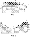
- Figure 1 shows a cross section (not to scale) of the element of the invention at the outer diameter of the element.
- a support 10 having four layers thereon.
- Recording layer 20 has thereon reflecting layer 30, a first protective layer 40 and a second protective layer 50.
- First protective layer 40 covers the annular portion 12 of the substrate not covered by recording layer 20 and reflective layer 30.
- the second protective layer covers the first protective layer at least in the region where it is desired to record information.
- first protective layer that extends beyond, and covers a portion of, the edge of the substrate. This is generally indicated by portion 42 of first protective layer 40. It was found that this extension of the protective layer substantially prevents unwanted chipping of the coated layers and substrate if the edge of the disk is subjected to an impact on a hard surface.
- Figure 2 is a cross section (again not to scale) of the element of the invention around the center hole, 14, of the disk.
- the second protective layer 50 can directly contact the reflective layer 30 near the center of the element. This is because the inner most portion of the recording layer of the disk is not used to record information. Thus, there is no need to improve the block error rate in this portion.
- second protective layer 50 extends over the entire surface of support 10.
- the element of the invention can have prerecorded ROM areas as described in US-A-4,940,618.
- the surface of the substrate can have a separate heat deformable layer as described in US-A-4,990,388.
- the single arm scratch tester consists of a platform upon which the disc to be tested is held.
- the platform and disk can be translated in a horizontal direction by a stepper motor.
- An arm is mounted on a pivot such that one end can be raised from or lowered to the disc surface.
- the end of the arm on the side of the pivot opposite from the disc contains a counterweight which maintains the arm in balance.
- a 102 mm diameter sapphire stylus is mounted on the underside of the arm.
- Calibrated brass weights can be mounted on the top side of the arm to create the desired load.
- the stylus is lowered gently to the disc surface.
- the arm and stylus are arranged so that when the stylus contacts the disc it is perpendicular to the surface.
- the disc is then translated under the stylus at a speed of approximately 25 mm/sec.
- a scratch of a particular depth is created.
- the arm is then translated a short distance (10 mm) in a direction perpendicular to the direction of the scratch.
- a new weight is mounted and the process repeated, creating a new scratch parallel to the original scratch. This procedure is repeated until the range of stylus load of interest is covered.
- the load is varied in steps of 5 grams, although other steps are possible, depending on the resolution desired.
- the resulting scratches are observed under a low power microscope. Failure is defined as the load at which delamination of any of the various layers is observed.
- BLER Block Error Rate
- a recordable CD disc was prepared according to methods known in the art (See, for example, US-A-4,990,388.) A dye which absorbs light with a wavelength in the vicinity of 780 nm was dissolved in a solvent and then applied to a polycarbonate substrate using a standard spin coating technique. This resulted in a coating of dye on the substrate all the way to the edge of the disk.
- the layer had a thickness of between 100 nm and 200 nm.
- the dye coated substrate was then placed in a vacuum chamber through which argon flows at a rate of about 40 sccm.
- Gold was then deposited on to the dye using a standard DC sputtering technique such that the gold layer had a thickness of about 100 nm.
- a thin (2 - 12 mm), UV curable lacquer (Diacure SD-17® from Dainippon Ink & Chemical, 35-58, 3-Chrome, Sakashita, Itabashi-Ku, Tokyo) was applied to the CD using a spin coating process.
- a disc was placed on a turntable (held by a vacuum chuck) and rotated at a low speed (50 - 150 RPM).
- the lacquer was applied to the center portion of the disc from a reservoir/pump system via a movable arm and small gage nozzle (14 - 17 ga) (corresponds to an inner diameter of 1.6 - 1 mm).
- This process results in the entire surface of the disc being covered by, in sequence, a recording layer of the dye, a reflective layer of gold and first protective layer of lacquer.
- the resulting disc was tested using a single arm scratch tester and failed when the stylus load exceeded 60 grams. This disc was then exposed to various edge impact forces. Chipping and delamination of the coated layers occurred when the edge of the disk was subjected to substantial impact against a hard surface.
- a disc was prepared as in the comparative example above except that after the dye was coated, and prior to the gold coating, the disc was subjected to an edge wash process. In this process the disc was caused to spin while a fluid capable of dissolving the dye was directed through a small gauge nozzle toward the outer diameter of the disc. This resulted in an annular ring approximately 1.4 mm wide, located at the very outer diameter of the disc, being free from dye.
- the disc was then placed in the vacuum system and the gold was sputtered onto the dye layer.
- the vacuum system had mounted in it a mask disposed so as to prevent gold from being deposited on the outer 0.7 mm annulus of the disc.
- Comparative Example 1 The process described in Comparative Example 1 was used to coat the lacquer layer over the entire disc surface. No chipping or delamination of the coated layers was observed after the disc was subjected to substantial edge impact. However, the scratch resistance of the disk was unchanged.
- the screen printing process begins by mounting a screen or mesh into a frame under tension.
- the screen was coated with a photographic emulsion into which the required image is exposed. This emulsion was then developed to form a positive image. In this case the image was simply a disc of dimension equal to that of the disk.
- the "mesh” of the screen corresponds to the number of threads per inch (which in turn, corresponds to threads per 2.54 cm). Thus, a lower “mesh” number indicates a more open screen and correspondingly, a thicker layer.
- a UV curable ink was applied to one side of the screen and a squeegee passed over the screen to equally fill the mesh openings with ink.
- the coated side of the disc was then brought into contact with the opposite side of the screen, resulting in the transfer of the ink from the screen to the disc.
- the ink was then cured by exposure to UV radiation. This cured ink layer comprises the second protective layer.
- the ink contained no pigmentation, and so was transparent and colorless.
- the ink can be modified by adding a particulate suspension (called a "matte").
- Discs were prepared using different degrees of matte, different thickness of ink (by changing the screen mesh), and inks from two manufacturers.
- the second durability layer had the following thicknesses, measured in micrometers:
- the second durability layer had the following thicknesses, measured in micrometers:
- a disc was prepared according to examples 10-19, except that the spin coating of the first protective layer began at a radius of about 22 mm. This created an annular ring of reflective layer between the radii of 19 and 22 mm which was free from the first protective layer. A disc identification code was written in this area, and then the second protective layer was screen printed over the entire disc surface. The durability of the disc within the recording area, as measured by the single arm scratch tester, was maintained.
- Discs were prepared in accordance with this invention, except that the first protective layer (the spin coated lacquer) began at a radius of about 30 mm. This caused the second protective layer (the screen printed "ink") to be in direct contact with the reflective layer in that portion of the recording region located at a radius of less than 30 mm. Digital information was recorded beginning at the inner recording radius (about 22 mm) and extending substantially past a radius of 35 mm.
- the first protective layer the spin coated lacquer
- the second protective layer the screen printed "ink”
- BLER Block Error Rate
- the BLER within the region where the second protective layer was in direct contact with the reflector layer was greater than 260 errors/sec. In the region where the second protective layer was separated from the reflector by the first protective layer the BLER was less than 40 errors/sec.
- Industry standards for CD audio discs require the BLER to be less than 200 errors/sec. No industry standard currently exists for BLER in CD data discs, but values of ⁇ 50 errors/sec are commonly specified. For comparison, discs prepared with the first and second protective layers covering the entire recording area had BLER of ⁇ 40 errors/sec.
- the durability of the disc in the area where the second protective layer was coated directly on to the gold reflector was determined using the single arm scratch tester.
- the average load to failure was 161 + 18 grams. This represents a significant reduction from the load to failure of 280 grams observed when both protective layers are present.
- Figure 1 is a schematic representation, in cross section, of an element of the invention at the outer edge of the element.
- Figure 2 is a schematic representation, in cross section, of an element of the invention near the center of the element.
Landscapes
- Manufacturing Optical Record Carriers (AREA)
- Optical Record Carriers And Manufacture Thereof (AREA)
Applications Claiming Priority (2)
| Application Number | Priority Date | Filing Date | Title |
|---|---|---|---|
| US815020 | 1985-12-30 | ||
| US07/815,020 US5312663A (en) | 1991-12-27 | 1991-12-27 | Optical element having durability enhancing layer |
Publications (3)
| Publication Number | Publication Date |
|---|---|
| EP0548968A2 true EP0548968A2 (de) | 1993-06-30 |
| EP0548968A3 EP0548968A3 (de) | 1993-08-04 |
| EP0548968B1 EP0548968B1 (de) | 1997-02-26 |
Family
ID=25216635
Family Applications (1)
| Application Number | Title | Priority Date | Filing Date |
|---|---|---|---|
| EP19920121939 Expired - Lifetime EP0548968B1 (de) | 1991-12-27 | 1992-12-23 | Optisches Aufzeichnungselement mit einer die Gebrauchsdauer steigernden Schicht |
Country Status (4)
| Country | Link |
|---|---|
| US (2) | US5312663A (de) |
| EP (1) | EP0548968B1 (de) |
| JP (1) | JPH05250725A (de) |
| DE (1) | DE69217637T2 (de) |
Cited By (7)
| Publication number | Priority date | Publication date | Assignee | Title |
|---|---|---|---|---|
| US5422226A (en) * | 1992-12-25 | 1995-06-06 | Mitsui Toatsu Chemicals, Inc. | Optical recording medium |
| EP0896328A1 (de) * | 1997-07-29 | 1999-02-10 | Victor Company Of Japan, Ltd. | Informationsaufzeichnungsträger und Verfahren zu dessen Herstellung |
| EP0915461A1 (de) * | 1997-10-31 | 1999-05-12 | Taiyo Yuden Co., Ltd. | Optisches Aufzeichnungsmedium und dessen Herstellungsverfahren |
| EP0874360A3 (de) * | 1997-04-23 | 2000-07-12 | Eastman Kodak Company | Verminderung von Wellen in optischen Aufzeichnungsplatten |
| EP1041549A4 (de) * | 1997-12-24 | 2004-12-22 | Tdk Corp | Optisches aufzeichnungsmedium und herstellungsverfahren dafür |
| EP1058250A4 (de) * | 1997-12-24 | 2004-12-22 | Tdk Corp | Otisches aufzeichnungsmedium und verfahren zu seiner herstellung |
| EP1343157A3 (de) * | 2002-03-07 | 2005-03-16 | Fuji Photo Film Co., Ltd. | Optisches Aufzeichnungsmedium |
Families Citing this family (27)
| Publication number | Priority date | Publication date | Assignee | Title |
|---|---|---|---|---|
| KR0185765B1 (ko) * | 1993-04-10 | 1999-04-15 | 가와다 미쓰구 | 광 정보매체와 그 제조방법 |
| JP2887083B2 (ja) * | 1994-12-02 | 1999-04-26 | 富士ゼロックス株式会社 | 熱記録型光学素子 |
| US5741836A (en) | 1994-12-22 | 1998-04-21 | Eastman Kodak Company | Screen-printable ink-receptive compositions |
| US5726969A (en) * | 1994-12-28 | 1998-03-10 | Matsushita Electric Industrial Co., Ltd. | Optical recording medium having dual information surfaces |
| US5470626A (en) * | 1995-02-21 | 1995-11-28 | Eastman Kodak Company | Optical recording layers containing sulfur |
| JP3079963B2 (ja) * | 1995-03-29 | 2000-08-21 | 日本ビクター株式会社 | 光ディスク及びその製造方法 |
| US5667860A (en) | 1995-11-14 | 1997-09-16 | Eastman Kodak Company | Optical recording elements having recording layers exhibiting reduced bubble formation |
| CN1190785C (zh) | 1996-09-24 | 2005-02-23 | 富士写真菲林株式会社 | 光信息记录盘 |
| JPH11203724A (ja) * | 1998-01-09 | 1999-07-30 | Sony Corp | 光ディスク及びその製造方法 |
| US6765652B1 (en) * | 1998-01-12 | 2004-07-20 | Micron Technology, Inc. | Forming thermally curable materials on a support structure in an electronic device |
| US6319580B1 (en) * | 1998-06-16 | 2001-11-20 | Hitachi Maxell, Ltd. | Recording disk and producing method therefor |
| US6242068B1 (en) | 1999-12-28 | 2001-06-05 | Eastman Kodak Company | Recordable optical media with a silver-palladium reflective layer |
| US6605195B2 (en) | 2000-04-14 | 2003-08-12 | Seagate Technology Llc | Multi-layer deposition process using four ring sputter sources |
| US6562432B2 (en) * | 2000-09-29 | 2003-05-13 | Ricoh Company, Ltd. | Optical recording medium and method of manufacturing the optical recording medium |
| EP1344212B1 (de) | 2000-12-14 | 2008-08-13 | ECD Systems, Inc. | Verfahren zur Authentifizierung eines optischen Aufzeichnungsmediums und ein optisches Aufzeichnungsmedium |
| TWI250514B (en) * | 2001-02-23 | 2006-03-01 | Tdk Corp | Method for making optical information medium and optical information medium |
| US7300690B2 (en) * | 2001-03-29 | 2007-11-27 | General Electric Company | Radial tilt reduced media |
| US7562396B2 (en) * | 2001-08-21 | 2009-07-14 | Ecd Systems, Inc. | Systems and methods for media authentication |
| US6716505B2 (en) * | 2001-08-31 | 2004-04-06 | General Electric Company | Storage medium for data with improved dimensional stability |
| US7643393B2 (en) | 2001-12-12 | 2010-01-05 | Ecd Systems, Inc. | Systems and methods for optical media modification |
| US7716485B2 (en) * | 2002-02-01 | 2010-05-11 | Sca Ipla Holdings Inc. | Systems and methods for media authentication |
| EP1505600A1 (de) * | 2003-07-30 | 2005-02-09 | Sony DADC Austria AG | Plattenförmiger optischer Aufzeichnungsträger |
| US20050112318A1 (en) * | 2003-11-20 | 2005-05-26 | Hsieh Timothy M. | Nanoparticles in optical devices |
| TWI363343B (en) * | 2003-12-10 | 2012-05-01 | Panasonic Corp | Optical information recording medium |
| JP2006085762A (ja) * | 2004-09-14 | 2006-03-30 | Fuji Photo Film Co Ltd | 光記録媒体 |
| JP4827848B2 (ja) * | 2005-08-30 | 2011-11-30 | パナソニック株式会社 | 多層情報記録媒体の製造方法、並びに多層情報記録媒体の製造装置とこの製造装置を構成する多層情報記録媒体製造用スクリーン |
| KR20110113623A (ko) * | 2008-12-31 | 2011-10-17 | 브라이엄 영 유니버시티 | 캡슐화된 데이터층을 포함하는 광학 데이터 저장 매체 |
Family Cites Families (12)
| Publication number | Priority date | Publication date | Assignee | Title |
|---|---|---|---|---|
| JPS6021555B2 (ja) * | 1978-06-29 | 1985-05-28 | 富士写真フイルム株式会社 | 熱的記録材料 |
| JPS57181443A (en) * | 1981-04-30 | 1982-11-08 | Toshiba Corp | Information storage medium |
| JPS58118045A (ja) * | 1981-12-29 | 1983-07-13 | Matsushita Electric Ind Co Ltd | 光学式記録円盤の塗装方法 |
| JPS6267742A (ja) * | 1985-09-20 | 1987-03-27 | Tdk Corp | 情報記録媒体 |
| JP2632671B2 (ja) * | 1986-06-24 | 1997-07-23 | 日本電気ホームエレクトロニクス株式会社 | 光デイスクの製造方法 |
| JPS63247935A (ja) * | 1987-04-02 | 1988-10-14 | Fuji Photo Film Co Ltd | 情報記録媒体の製造方法 |
| JPS6379169A (ja) * | 1987-04-17 | 1988-04-09 | Hitachi Ltd | 画像デ−タ取扱装置 |
| JPS6464147A (en) * | 1987-09-03 | 1989-03-10 | Sony Corp | Formation of protective film of magnetic recording medium |
| US4981743A (en) * | 1988-07-25 | 1991-01-01 | Unisys Corporation | Overcoat composition for optical record |
| DE69030982T2 (de) * | 1989-04-27 | 1997-11-13 | Canon Kk | Optisches Aufzeichnungsmedium und Verfahren zu seiner Herstellung |
| MY105953A (en) * | 1989-07-24 | 1995-02-28 | Taiyo Yuden Kk | Optical information recording medium and recording method. |
| WO1991010233A1 (en) * | 1990-01-05 | 1991-07-11 | Sims Steven C | Protective, vibration damping, stabilizer rings for optical discs |
-
1991
- 1991-12-27 US US07/815,020 patent/US5312663A/en not_active Ceased
-
1992
- 1992-12-23 EP EP19920121939 patent/EP0548968B1/de not_active Expired - Lifetime
- 1992-12-23 DE DE69217637T patent/DE69217637T2/de not_active Expired - Fee Related
- 1992-12-25 JP JP34668792A patent/JPH05250725A/ja active Pending
-
1994
- 1994-12-13 US US08/355,130 patent/USRE35947E/en not_active Expired - Lifetime
Cited By (9)
| Publication number | Priority date | Publication date | Assignee | Title |
|---|---|---|---|---|
| US5422226A (en) * | 1992-12-25 | 1995-06-06 | Mitsui Toatsu Chemicals, Inc. | Optical recording medium |
| EP0874360A3 (de) * | 1997-04-23 | 2000-07-12 | Eastman Kodak Company | Verminderung von Wellen in optischen Aufzeichnungsplatten |
| EP0896328A1 (de) * | 1997-07-29 | 1999-02-10 | Victor Company Of Japan, Ltd. | Informationsaufzeichnungsträger und Verfahren zu dessen Herstellung |
| US6083597A (en) * | 1997-07-29 | 2000-07-04 | Victor Company Of Japan, Ltd. | Information recording carrier and manufacturing method thereof |
| EP0915461A1 (de) * | 1997-10-31 | 1999-05-12 | Taiyo Yuden Co., Ltd. | Optisches Aufzeichnungsmedium und dessen Herstellungsverfahren |
| US6117512A (en) * | 1997-10-31 | 2000-09-12 | Taiyo Yuden Co., Ltd. | Optical information medium and manufacturing method therefor |
| EP1041549A4 (de) * | 1997-12-24 | 2004-12-22 | Tdk Corp | Optisches aufzeichnungsmedium und herstellungsverfahren dafür |
| EP1058250A4 (de) * | 1997-12-24 | 2004-12-22 | Tdk Corp | Otisches aufzeichnungsmedium und verfahren zu seiner herstellung |
| EP1343157A3 (de) * | 2002-03-07 | 2005-03-16 | Fuji Photo Film Co., Ltd. | Optisches Aufzeichnungsmedium |
Also Published As
| Publication number | Publication date |
|---|---|
| US5312663A (en) | 1994-05-17 |
| JPH05250725A (ja) | 1993-09-28 |
| DE69217637T2 (de) | 1997-09-25 |
| DE69217637D1 (de) | 1997-04-03 |
| EP0548968B1 (de) | 1997-02-26 |
| EP0548968A3 (de) | 1993-08-04 |
| USRE35947E (en) | 1998-11-03 |
Similar Documents
| Publication | Publication Date | Title |
|---|---|---|
| EP0548968B1 (de) | Optisches Aufzeichnungselement mit einer die Gebrauchsdauer steigernden Schicht | |
| US5325351A (en) | Optical recording medium having a reflective layer made of Cu-Ag or Cu-Au alloy | |
| EP0652555A2 (de) | Optisches Lesemedium | |
| EP0514799A1 (de) | Verfahren zur Herstellung eines optischen Aufzeichnungsmedium | |
| JPH11100527A (ja) | コーティング用組成物及び光記録媒体 | |
| KR100204455B1 (ko) | 광기록매체 | |
| JPH10154350A (ja) | 光学記録要素 | |
| JP3840345B2 (ja) | 光情報記録媒体 | |
| US5422226A (en) | Optical recording medium | |
| US6341122B1 (en) | Optical information recording medium | |
| JPH10151863A (ja) | 光学記録要素 | |
| EP0837460A1 (de) | Vierfach-Farbstoff vermischt mit wenigstens einem anderen Farbstoff für optische Aufzeichnungselemente | |
| JP3611438B2 (ja) | 光記録媒体及びその製造方法 | |
| EP2045805A1 (de) | Optisches Informationsaufzeichnungsmedium | |
| JPH10152623A (ja) | 金属化ホルマザン色素 | |
| JP2901417B2 (ja) | 光記録ディスクの製造方法 | |
| JPWO2003041068A1 (ja) | 光記録媒体 | |
| DE69837496T2 (de) | Optisches aufzeichnungsmedium und verfahren zu seiner herstellung | |
| US6858279B1 (en) | Process for producing optical recording medium and optical recording medium | |
| JP3556564B2 (ja) | 光記録媒体の製造方法及び光記録媒体 | |
| JPH08108623A (ja) | 光記録媒体 | |
| JPH08339573A (ja) | 光記録媒体 | |
| JP3246690B2 (ja) | 光記録方法 | |
| JP2648586B2 (ja) | 記録媒体 | |
| JP2000099998A (ja) | 光情報記録媒体及び該光情報記録媒体へのマーキング方法 |
Legal Events
| Date | Code | Title | Description |
|---|---|---|---|
| PUAI | Public reference made under article 153(3) epc to a published international application that has entered the european phase |
Free format text: ORIGINAL CODE: 0009012 |
|
| PUAL | Search report despatched |
Free format text: ORIGINAL CODE: 0009013 |
|
| AK | Designated contracting states |
Kind code of ref document: A2 Designated state(s): AT BE CH DE DK ES FR GB GR IE IT LI LU MC NL PT SE |
|
| AK | Designated contracting states |
Kind code of ref document: A3 Designated state(s): AT BE CH DE DK ES FR GB GR IE IT LI LU MC NL PT SE |
|
| 17P | Request for examination filed |
Effective date: 19940121 |
|
| GRAG | Despatch of communication of intention to grant |
Free format text: ORIGINAL CODE: EPIDOS AGRA |
|
| 17Q | First examination report despatched |
Effective date: 19960513 |
|
| GRAH | Despatch of communication of intention to grant a patent |
Free format text: ORIGINAL CODE: EPIDOS IGRA |
|
| RBV | Designated contracting states (corrected) |
Designated state(s): DE FR GB |
|
| GRAH | Despatch of communication of intention to grant a patent |
Free format text: ORIGINAL CODE: EPIDOS IGRA |
|
| GRAA | (expected) grant |
Free format text: ORIGINAL CODE: 0009210 |
|
| AK | Designated contracting states |
Kind code of ref document: B1 Designated state(s): DE FR GB |
|
| REF | Corresponds to: |
Ref document number: 69217637 Country of ref document: DE Date of ref document: 19970403 |
|
| ET | Fr: translation filed | ||
| PLBE | No opposition filed within time limit |
Free format text: ORIGINAL CODE: 0009261 |
|
| STAA | Information on the status of an ep patent application or granted ep patent |
Free format text: STATUS: NO OPPOSITION FILED WITHIN TIME LIMIT |
|
| 26N | No opposition filed | ||
| REG | Reference to a national code |
Ref country code: GB Ref legal event code: IF02 |
|
| PGFP | Annual fee paid to national office [announced via postgrant information from national office to epo] |
Ref country code: GB Payment date: 20051104 Year of fee payment: 14 |
|
| PGFP | Annual fee paid to national office [announced via postgrant information from national office to epo] |
Ref country code: FR Payment date: 20051201 Year of fee payment: 14 |
|
| PGFP | Annual fee paid to national office [announced via postgrant information from national office to epo] |
Ref country code: DE Payment date: 20051230 Year of fee payment: 14 |
|
| PG25 | Lapsed in a contracting state [announced via postgrant information from national office to epo] |
Ref country code: DE Free format text: LAPSE BECAUSE OF NON-PAYMENT OF DUE FEES Effective date: 20070703 |
|
| GBPC | Gb: european patent ceased through non-payment of renewal fee |
Effective date: 20061223 |
|
| REG | Reference to a national code |
Ref country code: FR Ref legal event code: ST Effective date: 20070831 |
|
| PG25 | Lapsed in a contracting state [announced via postgrant information from national office to epo] |
Ref country code: GB Free format text: LAPSE BECAUSE OF NON-PAYMENT OF DUE FEES Effective date: 20061223 |
|
| PG25 | Lapsed in a contracting state [announced via postgrant information from national office to epo] |
Ref country code: FR Free format text: LAPSE BECAUSE OF NON-PAYMENT OF DUE FEES Effective date: 20070102 |