EP0548982A2 - Démodulateur de phase non-cohérent utilisant une détection à délai - Google Patents
Démodulateur de phase non-cohérent utilisant une détection à délai Download PDFInfo
- Publication number
- EP0548982A2 EP0548982A2 EP92121972A EP92121972A EP0548982A2 EP 0548982 A2 EP0548982 A2 EP 0548982A2 EP 92121972 A EP92121972 A EP 92121972A EP 92121972 A EP92121972 A EP 92121972A EP 0548982 A2 EP0548982 A2 EP 0548982A2
- Authority
- EP
- European Patent Office
- Prior art keywords
- phase
- output
- signal
- exclusive
- frequency
- Prior art date
- Legal status (The legal status is an assumption and is not a legal conclusion. Google has not performed a legal analysis and makes no representation as to the accuracy of the status listed.)
- Granted
Links
Images








Classifications
-
- H—ELECTRICITY
- H04—ELECTRIC COMMUNICATION TECHNIQUE
- H04L—TRANSMISSION OF DIGITAL INFORMATION, e.g. TELEGRAPHIC COMMUNICATION
- H04L27/00—Modulated-carrier systems
- H04L27/18—Phase-modulated carrier systems, i.e. using phase-shift keying
- H04L27/22—Demodulator circuits; Receiver circuits
- H04L27/233—Demodulator circuits; Receiver circuits using non-coherent demodulation
- H04L27/2332—Demodulator circuits; Receiver circuits using non-coherent demodulation using a non-coherent carrier
-
- H—ELECTRICITY
- H03—ELECTRONIC CIRCUITRY
- H03D—DEMODULATION OR TRANSFERENCE OF MODULATION FROM ONE CARRIER TO ANOTHER
- H03D13/00—Circuits for comparing the phase or frequency of two mutually-independent oscillations
- H03D13/001—Circuits for comparing the phase or frequency of two mutually-independent oscillations in which a pulse counter is used followed by a conversion into an analog signal
-
- H—ELECTRICITY
- H03—ELECTRONIC CIRCUITRY
- H03D—DEMODULATION OR TRANSFERENCE OF MODULATION FROM ONE CARRIER TO ANOTHER
- H03D13/00—Circuits for comparing the phase or frequency of two mutually-independent oscillations
- H03D13/003—Circuits for comparing the phase or frequency of two mutually-independent oscillations in which both oscillations are converted by logic means into pulses which are applied to filtering or integrating means
-
- H—ELECTRICITY
- H03—ELECTRONIC CIRCUITRY
- H03D—DEMODULATION OR TRANSFERENCE OF MODULATION FROM ONE CARRIER TO ANOTHER
- H03D7/00—Transference of modulation from one carrier to another, e.g. frequency-changing
-
- H—ELECTRICITY
- H04—ELECTRIC COMMUNICATION TECHNIQUE
- H04L—TRANSMISSION OF DIGITAL INFORMATION, e.g. TELEGRAPHIC COMMUNICATION
- H04L27/00—Modulated-carrier systems
- H04L27/18—Phase-modulated carrier systems, i.e. using phase-shift keying
- H04L27/22—Demodulator circuits; Receiver circuits
- H04L27/233—Demodulator circuits; Receiver circuits using non-coherent demodulation
- H04L27/2335—Demodulator circuits; Receiver circuits using non-coherent demodulation using temporal properties of the received signal
- H04L27/2337—Demodulator circuits; Receiver circuits using non-coherent demodulation using temporal properties of the received signal using digital techniques to measure the time between zero-crossings
-
- H—ELECTRICITY
- H03—ELECTRONIC CIRCUITRY
- H03D—DEMODULATION OR TRANSFERENCE OF MODULATION FROM ONE CARRIER TO ANOTHER
- H03D2200/00—Indexing scheme relating to details of demodulation or transference of modulation from one carrier to another covered by H03D
- H03D2200/0041—Functional aspects of demodulators
- H03D2200/0066—Mixing
- H03D2200/007—Mixing by using a logic circuit, e.g. flipflop, XOR
-
- H—ELECTRICITY
- H03—ELECTRONIC CIRCUITRY
- H03D—DEMODULATION OR TRANSFERENCE OF MODULATION FROM ONE CARRIER TO ANOTHER
- H03D7/00—Transference of modulation from one carrier to another, e.g. frequency-changing
- H03D7/16—Multiple-frequency-changing
- H03D7/161—Multiple-frequency-changing all the frequency changers being connected in cascade
-
- H—ELECTRICITY
- H03—ELECTRONIC CIRCUITRY
- H03D—DEMODULATION OR TRANSFERENCE OF MODULATION FROM ONE CARRIER TO ANOTHER
- H03D7/00—Transference of modulation from one carrier to another, e.g. frequency-changing
- H03D7/16—Multiple-frequency-changing
- H03D7/165—Multiple-frequency-changing at least two frequency changers being located in different paths, e.g. in two paths with carriers in quadrature
Definitions
- This invention relates to delayed detection type demodulators used in the radio communication systems, and more particularly to the improvements in the frequency converter and the phase comparator or the phase detection circuit used in the delayed detection type demodulators.
- a conventional delayed detection type demodulator provided with a frequency converter and a phase comparator is disclosed, for example, in Japanese Laid-Open Patent (Kokai) No. 64-12646, "DPSK demodulation system". Next, this delayed detection type demodulator is described by reference to Fig. 8.
- the frequency converter 20 includes a multiplier 21 and a low pass filter 22.
- the phase comparator 30 includes: a phase shifter 31 for shifting the phase of the local carrier (the phase reference signal) by ⁇ /2 radians; a multiplier 32 for multiplying the local carrier by the output of the low pass filter 22; a multiplier 33 for multiplying the output of the phase shifter 31 by that of the low pass filter 22; a low pass filter 34 for removing the high frequency components from the output of the multiplier 32; a low pass filter 35 for removing the high frequency components from the output of the multiplier 33; a sampler 36 for sampling the output of the low pass filter 34; a sampler 37 for sampling the output of the low pass filter 35; and a coordinate converter 38 for calculating and generating a relative phase signal from the outputs of the samplers 36 and 37.
- a delay element 40 delays the relative phase signal by one symbol period of the received signal.
- a subtractor 41 subtracts, in modulo 2 ⁇ , the relative phase signal delayed by one symbol period by the delay element 40 from the relative phase signal directly output from the coordinate converter 38.
- a judgment circuit 42 outputs the demodulated data corresponding to the values of the inter-symbol phase shift differences.
- the received signal is a differential phase shift keying (DPSK) signal.
- DPSK differential phase shift keying
- This received signal is input to the frequency converter 20, where the multiplier 21 multiplies it by the signal for frequency conversion. It is assumed that the frequency of the received signal is 1 1 Hz and that of the frequency conversion signal f 2 Hz.
- the multiplied signal output from the multiplier 21 includes a high frequency component at 1 1 + f 2 Hz and a low frequency component at
- This multiplied signal output from the multiplier 21 is supplied to the low pass filter 22, where the high frequency component is suppressed and only the low frequency component at
- the received signal thus undergoes the frequency conversion.
- the received signal is processed by the phase comparator 30.
- the multiplier 32 multiplies the received signal after the frequency conversion (output from the frequency converter 20) by the phase reference signal (the local carrier).
- the low pass filter 34 removes the high frequency components from the output of the multiplier 32, thereby obtaining the base band signal in phase with the local carrier (referred to as the in-phase base band signal).
- the phase shifter 31 shifts the phase of the phase reference signal or the local carrier by ⁇ /2 radians.
- the multiplier 33 multiplies the received signal after the frequency conversion (output from the frequency converter 20) by the output of the phase shifter 31.
- the low pass filter 35 removes the high frequency components from the output of the multiplier 33, thereby obtaining the base band signal in quadrature with the local carrier (referred to as the quadrature base band signal).
- the in-phase base band signal output from the low pass filter 34 is sampled by the sampler 36 and supplied to the coordinate converter 38.
- the quadrature base band signal output from the low pass filter 35 is sampled by the sampler 37 and supplied to the coordinate converter 38.
- the coordinate converter 38 outputs the relative phase signal representing the phase shift of the received signal after frequency conversion relative to the local carrier or the phase reference signal.
- the value of the relative phase signal 0 is expressed by the values x and y of the sampled in-phase and quadrature base band signals as follows:
- the relative phase signal output from the coordinate converter 38 is supplied to the subtractor 41 and the delay element 40.
- the relative phase signal is delayed by one symbol period of the received signal and then is supplied to the subtractor 41.
- the subtractor 41 subtracts, in modulo 2 ⁇ , the output of the delay element 40 from the output of the coordinate converter 38, and thereby obtains the phase shift difference signal (abbreviated hereinafter to phase difference signal).
- the phase difference signal output from the subtractor 41 represents the phase transition over each symbol period of the received signal.
- the judgment circuit 42 obtains the demodulated data on the basis of the predetermined correspondence relationship between the inter-symbol phase difference signal and the demodulated data.
- the above conventional delayed detection type demodulator has the following disadvantage. Since the frequency converter and the phase comparator circuits are composed of analog elements, integration of circuit elements into ICs is difficult. Thus, the adjustment or tuning of the circuits is indispensable. Further, it is difficult to reduce the size and the power consumption of the circuit.
- a frequency converter circuit for converting a frequency of a first two-valued signal using a second two-valued signal having a frequency distinct from the frequency of the first signal, comprising: an exclusive OR element for obtaining a logical exclusive OR of the first and second signal; shift average generator means, coupled to the exclusive OR element, for generating a signal corresponding to k times a shift average of an output of the exclusive OR element, k being a positive integer; and judgment means, coupled to the shift average generator means, for converting an output of the shift average generator means to a two-valued logical signal.
- the shift average generator means comprises: a shift register coupled to the exclusive OR element and having (2n + 1) stages to hold respective bits, where n is a positive integer and the output of the exclusive OR element is first supplied to a first stage of the shift register, the shift register shifting the bits held in the stages from the first toward (2n + 1 )th stage in synchronism with a clock having a period substantially shorter than periods of the first and second signals; and an adder means coupled to the shift register, for adding bits of the respective stages of the shift register, wherein an output of the adder constituting the output of the shift average generator means.
- the shift average generator means comprises: a shift register coupled to the exclusive OR element and having (2n + 2) stages to hold respective bits, where n is a positive integer and the output of the exclusive OR element is first supplied to a first stage of the shift register, the shift register shifting the bits held in the stages from the first toward (2n + 2)th stage in synchronism with a clock having a period substantially shorter than periods of the first and second signals; a sign invertor coupled to the shift register, for inverting a polarity of an output bit of the (2n + 2)th stage; an adder coupled to the first stage of the shift register and the sign invertor; and a delay element having an input coupled to an output of the adder and having an output coupled to an input of the adder, the delay element delaying the output of the adder in synchronism with the clock of the shift register; wherein the adder adds outputs of: the first stage of the shift register; the sign invertor; and the delay element, the output of the delay element constituting the output of the
- the judgment means compares the output of the shift average generator means with a predetermined threshold level to convert the output of the shift average generator means to the two-valued logical signal.
- phase comparator for determining a phase shift of a two-valued received signal relative to a phase reference signal having a fixed frequency substantially equal to a frequency of the received signal
- the phase comparator comprising: an exclusive OR element for obtaining a logical exclusive OR of the received signal and the phase reference signal; absolute phase shift measurement means coupled to the exclusive OR element, for determining a duration in which an output of the exclusive OR element is sustained at a logical "1" during each half period of the phase reference signal; and phase shift polarity judgment means coupled to the exclusive OR element, for judging whether the phase of the received signal is delayed or advanced with reference to the phase reference signal, on the basis of a value of the exclusive OR element at each half period of the phase reference signal; wherein a combination of outputs of the absolute phase shift measurement means and the phase shift polarity judgment means represents the phase shift of the received signal relative to the phase reference signal.
- the absolute phase shift measurement means comprises: an adder coupled to the exclusive OR element; and a delay element having an input coupled to an output of the adder and having an output coupled to an input of the adder, the delay element delaying the output of the adder in synchronism with a clock having a period substantially shorter than the period of the phase reference signal, the delay element being reset at each half period of the phase reference signal; wherein the adder adds outputs of the exclusive OR element and the delay element to obtain a value corresponding to the duration in which the output of the exclusive OR element is sustained at a logical "1" during each half period of the phase reference signal.
- the delayed detection type demodulator acccording to this invention for demodulating a two-valued received signal using a phase reference signal having a fixed frequency substantially equal to a frequency of the received signal comprises: a phase comparator including: an exclusive OR element for obtaining a logical exclusive OR of the received signal and the phase reference signal; absolute phase shift measurement means coupled to the exclusive OR element, for determining a duration in which an output of the exclusive OR element is sustained at a logical "1" during each half period of the phase reference signal; and phase shift polarity judgment means coupled to the exclusive OR element, for judging whether the phase of the received signal is delayed or advanced with reference to the phase reference signal, on the basis of a value of the exclusive OR element at each half period of the phase reference signal; wherein a combination of outputs of the absolute phase shift measurement means and the phase shift polarity judgment means constituting a relative phase signal output from the phase comparator; a delay element coupled to the phase comparator, for delaying the relative phase signal output from the phase comparator
- the delayed detection type demodulator for demodulating a first two-valued signal using a phase reference signal having a fixed frequency substantially equal to a frequency of the first signal
- the delayed detection type demodulator comprises: a frequency converter circuit for converting the frequency of the first signal using a second two-valued signal having a frequency distinct from the frequency of the first signal, including: an exclusive OR element for obtaining a logical exclusive OR of the first and second signal; shift average generator means, coupled to the exclusive OR element, for generating a signal corresponding to k times a shift average of an output of the exclusive OR element, k being a positive integer; and judgment means, coupled to the shift average generator means, for converting an output of the shift average generator means to a two-valued logical signal, an output of the judgment means constituting an output of the frequency converter; a phase comparator including: an exclusive OR element coupled to the judgment means of the frequency converter, for obtaining a logical exclusive OR of the output the frequency converter the received signal and the phase reference signal; absolute
- the phase detection circuit for detecting a phase shift of an input signal relative to a phase reference signal, comprises: half-period detector means for generating, in response to the input signal, a half-period detection signal at each half-period of the input signal;phase reference signal generator means for generating the phase reference signal in response to a clock having a frequency not less than twice a frequency of the input signal; and phase shift determiner means, coupled to the half-period detector means and phase reference signal generator means and including phase inversion corrector means for correcting the phase reference signal for a phase inversion thereof at each alternate half-period of the input signal, the phase shift determiner means determining and outputting a phase shift of the input signal with respect to the phase reference signal at each half-period of the input signal, on the basis of the phase reference signal corrected by the phase inversion corrector means and the half-period detection signal output from the half-period detector means.
- the half-period detector means includes: a delay element for delaying the input signal by a delay time shorter than the half-period of the input signal; and a first exclusive OR element for generating a logical exclusive OR of the input signal and an output of the delay element;
- the phase reference signal generator means includes a counter for counting in modulo 2N a clock having a frequency substantially equal to 2N times the frequency of the input signal, where N is a positive integer;
- the phase inversion corrector means adds a numerical value "0" or "N” in modulo 2N to an output of the counter in response to the output of the delay element;
- the phase shift determiner means includes, in addition to the phase inversion corrector means, a D flip-flop array coupled to the phase inversion corrector means and the first exclusive OR element, the D flip-flop array holding an output of the phase inversion corrector means in response to the logical exclusive OR output of the exclusive OR element, wherein a value held in the D flip-flop array constitutes an output of the phase shift determine
- phase inversion corrector means may include: a multiplier coupled to the delay element, for multiplying the output of the delay element by N; and an adder coupled to the counter and the multiplier, for adding an output of the multiplier to the output of the counter in modulo 2N.
- the phase inversion corrector means may include: a data selector coupled to the delay element, for selecting a numerical value "0" when the output of the delay element is at logical "0", and a numerical value "1" when the output of the delay element is at logical "1 "; and an adder coupled to the counter and the data selector, for adding an output of the data selector to the output of the counter in modulo 2N.
- the phase inversion corrector means may include: logical product elements coupled to the delay element, for generating logical products of the output of the delay element and respective bits of a numerical value "N"; and an adder coupled to the counter and the logical product elements, for adding outputs of the logical product elements with the output of the counter in modulo 2N.
- the counter counts a clock having a frequency substantially equal to 2M times the frequency of the input signal, where M is a positive integer; and the phase inversion corrector means includes a second exclusive OR element coupled to the output of the delay element and a most significant bit of the output of the counter, the second exclusive OR element generating a logical exclusive OR of the output of the delay element and the most significant bit of the output of the counter, wherein an output of the phase inversion corrector means consists of a combination of least significant bits of the output of the modulo 2N counter and the logical exclusive OR output of the second exclusive OR element.
- the delayed detection type demodulator for demodulating a two-valued received signal using a phase reference signal having a fixed frequency substantially equal to a frequency of the received signal
- the delayed detection type demodulator comprises: half-period detector means for generating, in response to the received signal, a half-period detection signal at each half-period of the received signal; phase reference signal generator means for generating the phase reference signal in response to a clock having a frequency not less than twice the frequency of the received signal, phase shift determiner means, coupled to the half-period detector means and phase reference signal generator means and including phase inversion corrector means for correcting the phase reference signal for a phase inversion thereof at each alternate half-period of the received signal, the phase shift determiner means outputting a relative phase signal representing a relative phase of the received signal with respect to the phase reference signal at each half-period of the received signal, on the basis of the phase reference signal corrected by the phase inversion corrector means and the half-period detection signal
- the method according to this invention for detecting a phase shift of an input signal relative to a phase reference signal comprises the steps of: generating, in response to the input signal; a half-period detection signal at each half-period of the input signal; generating the phase reference signal in response to a clock having a frequency not less than twice a frequency of the input signal; correcting the phase reference signal for a phase inversion thereof at each alternate half-period of the input signal; and determining a phase shift of the input signal with respect to the phase reference signal at each half-period of the input signal, on the basis of the corrected phase reference signal and the half-period detection signal.
- a frequency converter circuit for converting a frequency of an input signal utilizing a signal for frequency conversion, wherein the frequency converter circuit comprises: a multiplier means for multiplying the input signal by the signal for frequency conversion; and a sampler means for sampling an output of the multiplier means at a frequency twice a frequency of the signal for frequency conversion.
- Fig. 1 is a block diagram showing the circuit structure of a delayed detection type demodulator provided with a frequency converter and a phase comparator according to this invention.
- a limiter amplifier 10 subjects the received signal to a two-value quantization.
- a frequency converter 50 coupled to the limiter amplifier 10 effects a frequency conversion on the two-value quantized received signal output from the limiter amplifier 10.
- the frequency converter 50 is organized as follows.
- An exclusive OR element 51 is coupled to the limiter amplifier 10 to obtain the logical exclusive OR of the output of the limiter amplifier 10 and the signal for frequency conversion (the frequency conversion signal).
- a shift average generator 52 removes the high frequency variation components from the output of the exclusive OR element 51.
- the shift average generator 52 includes: a shift register 53 for sequentially delaying the output of the exclusive OR element 51; and an adder 54 for adding the output bits of the shift register 53.
- a comparator 55 coupled to the adder 54 compares the output of the adder 54 with a predetermined threshold value.
- a phase comparator 60 is coupled to the frequency converter 50 to compare the phase of output of the frequency converter 50 (the received signal after subjected to the frequency conversion) and the phase of the phase reference signal.
- the phase comparator 60 is organized as follows.
- An exclusive OR element 61 coupled to the comparator 55 effects the logical exclusive OR operation upon the output of the comparator 55 and the phase reference signal.
- an absolute phase shift measurement means 62 determines the absolute value of the phase shift of the received signal after frequency conversion relative to the phase reference signal.
- the absolute phase shift measurement means 62 includes an adder 63 coupled to the exclusive OR element 61 and a pair of D flip-fops 64 and 65 coupled to the adder 63.
- the output of the D flip-flop array 64 delaying the output of the adder 63, is returned to the adder 63.
- the adder 63 adds the outputs of the exclusive OR element 61 and the D flip-flop array 64.
- the D flip-flop array 65 stores the output of the adder 63.
- the phase comparator 60 further includes a D flip-flop 66. In response to the output of the exclusive OR element 61, the D flip-flop 66 judges whether the phase of the received signal after frequency conversion is advanced or retarded relative to the phase reference signal. The bits output from the D flip-fops 65 and 66 are combined to obtain the output of the phase comparator 60 (i.e., the relative phase signal).
- the output of the phase comparator 60 is supplied to the subtractor 41 and the delay element 40.
- the relative phase signal is delayed by one symbol period of the received signal and then is supplied to the subtractor 41.
- the subtractor 41 subtracts, in modulo 2 7 r , the output of the delay element 40 from the output of the phase comparator 60, and thereby obtains the phase difference signal.
- the judgment circuit 42 obtains the demodulated data on the basis of the predetermined correspondence relationship between the phase difference signal and the demodulated data.
- the limiter amplifier 10 shapes the received signal into a rectangular waveform of a constant amplitude. Namely, the limiter amplifier 10 acts as a two-valued quantizer for subjecting the received signal to the two-value quantization, such that the output of the limiter amplifier 10 is quantized to logical "0" and "1".
- the two-value quantized output of the limiter amplifier 10 is supplied to the frequency converter 50, where the exclusive OR element 51 effects the logical exclusive OR operation upon the output of the limiter amplifier 10 and the signal for frequency conversion (the frequency conversion signal) which also takes either the logical value "0" or "1".
- the exclusive OR element 51 acts as a multiplier for multiplying the output of the limiter amplifier 10 (the two-value quantized received signal) by the signal for frequency conversion.
- the output of the exclusive OR element 51 is then supplied to the shift register 53 having (2n + 1) stages to hold respective bits, where n is a positive integer.
- the frequency of the clock signal for driving the shift register 53 is assumed to be higher than the frequency of the output of the limiter amplifier 10 and the frequency of the signal for frequency conversion.
- the (2n + 1) bits output from the respective stages of the shift register 53 are supplied to the adder 54.
- the period of the clock for the shift register 53 be T c .
- the output of the adder 54 constitutes the output of the shift average generator 52, which is supplied to the comparator 55.
- the comparator 55 compares the output of the shift average generator 52 with the constant n. Depending on the value b i of the output of the shift average generator 52 and the constant n, the value d i of the output signal of the comparator 55 is given as follows:
- the comparator 55 acts as a judgment means for converting the output b i of the shift average generator 52 into a two-valued signal which takes either of the two logical values "0" and "1".
- the signal processing within the frequency converter 50 thus converts the frequency of the two-value quantized received signal (output of the limiter amplifier 10). Namely, if the frequency of the two-value quantized received signal is represented by f 1 Hz, that of the signal for frequency conversion by f 2 Hz, then the frequency of the received signal after frequency conversion (the output of the frequency converter 50) is:
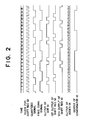
- the waveforms shown below the time scale are, from top to bottom: the clock that drives the shift register 53; the output of the limiter amplifier 10 (the two-value quantized received signal); the signal for frequency conversion (the frequency conversion signal); the output of the exclusive OR element 51; the first bit of the shift register 53; the fifth bit of the shift register 53, the output of the adder 54 (the inserted numbers representing the values of the output); and the output of the comparator 55. It is assumed that all the five bits of the shift register 53 are at logical "0" at time "1".
- the frequency of the clock driving the shift register 53 be f 0 Hz.
- the frequency f 1 of the two-value quantized received signal (the output of the limiter amplifier 10 supplied to the frequency converter 50) and the frequency f 2 of the signal for frequency conversion are given by:
- the frequency f 3 of the output of the frequency converter 50 (the received signal after frequency conversion)
- the frequency f 1 of the output of the limiter amplifier 10 (the two-value quantized received signal)
- the frequency f 2 of the signal for frequency conversion satisfy:
- the waveforms of the two-value quantized received signal and the frequency conversion signal (the signal for frequency conversion) can be interchanged without affecting the waveforms of the output waveforms of the exclusive OR element 51, the shift register 53, the adder 54 and the comparator 55.
- the frequency f o of the clock for the shift register 53, the frequency f 1 of the two-value quantized received signal, and the frequency f 2 of the signal for frequency conversion satisfy:
- the frequency f 3 of the received signal after frequency conversion are expressed in terms of the frequencies f 1 and f 2 as follows:
- the output of the exclusive OR element 51 includes a high frequency variation component at fo/2 Hz.
- the output of the comparator 55 does not include variation components at such high frequency.
- the shift average generator 52 consisting of the shift register 53 and the adder 54, and the comparator 55 acting as the judgment means for converting the output of the shift average generator 52 into a two-valued logical signal, function together as a low pass filter for removing the high frequency components from the output of the exclusive OR element 51.
- the output of the frequency converter 50 (the received signal after the frequency conversion) is supplied to the phase comparator 60.
- the exclusive OR element 61 effects the exclusive OR operation upon the received signal after the frequency conversion and the phase reference signal which is a two-valued signal taking either the logical "0" or "1".
- the exclusive OR element 61 acts as a multiplier for multiplying the received signal after the frequency conversion by the phase reference signal.
- the duration during which the output of the exclusive OR element 61 is continuously sustained at the logical "1" " is proportional to the absolute value of the phase shift of the received signal after the frequency conversion relative to the phase reference signal.
- Fig. 3 is a timing chart showing the waveforms of the phase reference signal, the received signal after the frequency conversion, and the output of the exclusive OR element 61 of Fig. 1, in the two cases where the received signal after frequency conversion is advanced (shown above) and delayed (shown below) with respect to the phase reference signal.
- the absolute value of the phase shift of the received signal after frequency conversion relative to the phase reference signal is expressed in terms of: the length of time 7 between the leading or trailing edges of the received signal after frequency conversion and the phase reference signal; and the period T of the phase reference signal. Namely, the absolute value of the phase shift is expressed as follows:
- the time 7 between the leading or the trailing edges of the phase reference signal and the received signal after frequency conversion is equal to the time during which the output of the exclusive OR element 61 is continuously sustained at logical "1".
- the duration by which the output of the exclusive OR element 61 is sustained at logical "1" " is proportional to the absolute value of the phase shift of the received signal after frequency conversion relative to the phase reference signal. Consequently, the absolute value of the phase shift of the received signal after frequency converter relative to the phase reference signal can be determined by measuring the duration in which the output of the exclusive OR element 61 is continuously sustained at logical "1".
- the output of the exclusive OR element 61 is supplied to the absolute phase shift measurement means 62, where the adder 63 adds the outputs of the exclusive OR element 61 and the D flip-flop array 64, the output of the adder 63 being supplied to the D flip-flop array 64 and the D flip-flop array 65.
- the frequency of the clock which drives the D flip-flop array 64 is selected at M times the frequency of the phase reference signal, where M is an even number not less than four.
- the D flip-flop array 64 acts as a delay element for storing the output of the adder 63.
- the output of adder 63 is incremented by one over each period of the clock of the D flip-flop array 64.
- the output of the adder 63 remains constant.
- the output of the adder 63 is also input to the D flip-flop array 65.
- the frequency of the clock of the D flip-flop array 65 is two times that of the phase reference signal, the leading edges of the clock of the D flip-flop array 65 coinciding with the leading or the trailing edges of the phase reference signal.
- the D flip-flop array 64 is reset at the rising edge of the clock for the D flip-flop array 65. Namely, the D flip-flop array 64 is reset at each half period of the phase reference signal.
- the output of the D flip-flop array 65 is thus equal to the integral part of the duration of logical "1" " of the output of the exclusive OR element 61 during each half period of the phase reference signal, as measured by the periods of the clock of the D flip-flop array 64. Namely, the output of the D flip-flop array 65 is obtained by dividing the duration of the logical "1" " of the exclusive OR element 61 by the length of the period of the clock of the D flip-flop array 64 and then discarding the fractional part of the quotient resulting from the division.
- Fig. 5 is a timing chart showing the same waveforms as those of Fig. 4, occurring when the received signal after the frequency conversion is delayed relative to the phase reference signal. In Figs.
- the numbers shows at the last three waveforms are the values thereof at respective time intervals.
- the frequency of the clock of the D flip-flop array 65 is two times that of the clock of the phase reference signal. Further, the D flip-flop array 64 is reset at respective leading edges of the clock of the D flip-flop array 65. Furthermore, as described above, the output of the D flip-flop array 65 is obtained by normalizing the duration of the logical "1" " of the exclusive OR element 61 during each half period of the phase reference signal by the length of the period of the clock of the D flip-flop array 64 and then discarding the fractional parts of the normalized value.
- the value of the output of the D flip-flop array 65 be represented by ⁇ , where ⁇ is an integer ranging from 0 to M/2 ( u ⁇ ⁇ 0, 1, ..., M/2 ⁇ ). Then, the following relationship holds among: the output u of the D flip-flop array 65, the ratio M of the frequency of the clock of the D flip-flop array 64 to the frequency of the clock of the phase reference signal, and the absolute value of the phase shift of the received signal after frequency conversion relative to the phase reference signal:
- the value ⁇ of the output of the absolute phase shift measurement means 62 is approximately equal to the absolute value of the phase shift of the received signal after frequency conversion relative to the phase reference signal, and the error is not greater than ⁇ 7 r/M.
- the measurement error of the absolute value of the phase shift can be reduced arbitrarily.
- the absolute value of the phase shift of the received signal after the frequency conversion relative to the phase reference signal is thus measured by the absolute phase shift measurement means 62. If the sign bit representing the positive or the negative sign is added to the measurement value ⁇ in correspondence with the phase delay or the phase advance of the received signal after the frequency conversion relative to the phase reference signal, then the phase shift of the received signal after frequency conversion relative to the phase reference signal can adequately be represented.
- the value of the output of the exclusive OR element 61 at each leading edge of the clock of the D flip-flop array 65 corresponds to the delay or the advance of the phase of the received signal after frequency conversion relative to the phase reference signal.
- the output of the exclusive OR element 61 is supplied to the D flip-flop 66 which is driven by the same clock as the D flip-flop array 65, such that the output of the D flip-flop 66 represents whether the phase of the received signal after frequency conversion is delayed or advanced relative to the phase reference signal.
- Fig. 6 is a timing chart showing the waveforms related to the operation of the D flip-flop 66 of Fig. 1. From top to bottom in Fig. 6, are shown the waveforms of: the clock for driving the D flip-flop 66; the phase reference signal; the received signal after frequency conversion; the output of the exclusive OR element 61; and the output of the D flip-flop 66.
- the clock of the D flip-flop 66 is the same as the clock of the D flip-flop array 65. Namely, the frequency of the clock of the D flip-flop 66 is two times that of the phase reference signal, the leading edges of the clock of the D flip-flop 66 coinciding with the leading or the trailing edges of the phase reference signal.
- the D flip-flop 66 judges at the edge of each half period of the phase reference signal whether the received signal after frequency conversion is delayed or advanced relative to the phase reference signal.
- the output of the D flip-flop 66 constitutes the sign bit representing the polarity of the phase shift of the received signal after frequency conversion relative to the phase reference signal.
- the output of the D flip-flop 66 is combined with the output of the absolute phase shift measurement means 62 to form together the output of the phase comparator 60.
- the output of the phase comparator 60 is a combination of the outputs of the absolute phase shift measurement means 62 and the D flip-flop 66.
- the output of the phase comparator 60 is the relative phase signal which represents absolute value of the phase shift of the received signal after frequency conversion relative to the phase reference signal.
- the relative phase signal output from the phase comparator 60 is delayed by the delay element 40 by one symbol period of the received signal, and thence is supplied to the subtractor 41.
- the relative phase signal is also supplied to the subtractor 41 of modulo 2-ff.
- the subtractor 41 Upon receiving the outputs of the phase comparator 60 and the delay element 40, the subtractor 41 subtracts, in modulo 2 7 r, the output of the delay element 40 from the output of the phase comparator 60, and thereby obtains the inter-symbol phase difference signal, which represents the phase transition over each symbol period of the received signal.
- the inter-symbol phase difference signal output from the subtractor 41 is supplied to the judgment circuit 42.
- the judgment circuit 42 obtains the demodulated data corresponding to the value of the inter-symbol phase difference signal, on the basis of the predetermined correspondence relationship between the inter-symbol phase difference signal and the demodulated data.
- the constant n may be any positive integer.
- Fig. 7 is a block diagram showing the circuit structure of another delayed detection type demodulator according to this invention.
- the circuit is similar to that of Fig. 1 except for the structure of the shift average generator 52a of the frequency converter 50a.
- the shift average generator 52a includes: a shift register 53a provided with (2n + 2) stages (first through (2n + 2)th stages to hold respective bits), where n is a positive integer and the bits are sequentially shifted from the first toward the (2n + 2)th bit in synchronism with the clock of the shift register 53a; and an adder 54a for adding the first bit of the shift register 53a and the outputs of a sign invertor 56 and a D flip-flop 57.
- the sign invertor 56 inverts the polarity of the (2n + 2)th bit of the shift register 53a and supplies the result to the adder 54a.
- the D flip-flop 57 coupled to the output of the adder 54a serves as a delay element for storing the output of the adder 54a. The output of the D flip-flop 57 is supplied to the adder 54a.
- the limiter amplifier 10 quantizes the received signal into a two-value quantized signal taking either the logical "0" or "1".
- the two-value quantized received signal output from the limiter amplifier 10 is supplied to the frequency converter 50a, in which the exclusive OR element 51 effects logical exclusive OR operation upon the output of the limiter amplifier 10 (the two-value quantized received signal) and the signal for frequency conversion (the frequency conversion signal) which also takes either the logical value "0" or "1".
- the exclusive OR element 51 acts as a multiplier for multiplying the output of the limiter amplifier 10 (the two-value quantized received signal) by the signal for frequency conversion.
- the output of the exclusive OR element 51 is supplied to the first stage of the shift register 53a, from whence it is shifted toward the (2n + 2)th stage in synchronism with the clock of the shift register 53a.
- the frequency of the clock of the shift register 53a is substantially greater than the frequencies of the two-value quantized received signal and the signal for frequency conversion.
- the first bit of the shift register 53a is input to the adder 54a.
- the (2n + 2)th bit of the shift register 53a is input to the sign invertor 56, where the sign or polarity thereof is inverted and thence supplied to the adder 54a.
- the output of the D flip-flop 57 is also supplied to the adder 54a.
- the adder 54a adds the first bit of the shift register 53a, the output of the sign invertor 56, and the output of the D flip-flop 57, and outputs the result to the D flip-flop 57.
- the D flip-flop 57 serves as the delay element for storing the output of the adder 54a.
- the clock of the D flip-flop 57 be the same as that of the shift register 53a.
- the sign invertor 56 inverts the polarity of the (2n + 2)th bit output from the shift register 53a.
- the output s i of the D flip-flop 57 for 1 ⁇ i ⁇ 2n + 1 is thus expressed as:
- the value s 2n+1 is equal to (2n + 1) times the average of the preceding (2n + 1) output values aoo, a 01 , ..., a 0(2n) , of the exclusive OR element 51. From this it can be shown that the following relation holds for t (2n + 1) T c :
- the output s i of the D flip-flop 57 is equal to (2n + 1) times the average of preceding (2n + 1) output values, a 0(i-2n-1) , a 0(i-2n), ..., a 0(i-1) , of the exclusive OR element 51.
- This output s i of the D flip-flop 57 constitutes the output of the shift average generator 52a.
- the shift average generator 52A functions similarly to the shift average generator 52 of Fig. 1.
- the number of the signals input to the adder 54a is three, irrespective of the number of the stages of the shift register 53a.
- the number of signals input to the adder 54 is equal to the number of stages, (2n + 1), of the shift register 53. Since n is greater than one (n 1) and hence (2n + 1) ⁇ 3, the number of signals input to the adder 54a is not greater than (and generally substantially less than) the number of signals input to the adder 54 in the circuit of Fig. 1.
- the circuit of the embodiment of Fig. 7 is simplified.
- the output of the shift average generator 52a is supplied to the comparator 55.
- the comparator 55 compares the output of the shift average generator 52a with the constant n. Depending on the value s i of the output of the shift average generator 52a and the constant n, the value d i of the output signal of the comparator 55 is given as follows:
- the comparator 55 acts as a judgment means for converting the output s i of the shift average generator 52a into a two-valued signal which takes either the logical value "0" or "1".
- the signal processing within the frequency converter 50a subsequent to the shift average generator 52a is identical to that subsequent to the shift average generator 52 in Fig. 1.
- the shift average generator 52a acts in a similar manner as the shift average generator 52 of Fig. 1.
- the shift average generator 52a consisting of the shift register 53a, the adder 54a, the sign invertor 56, and the D flip-flop 57, and the comparator 55 acting as the judgment means for converting the output of the shift average generator 52a into a two-valued logical signal, function as a low pass filter for removing the high frequency components from the output of the exclusive OR element 51.
- the two-value quantized received signal output from the limiter amplifier 10 is subjected to the frequency conversion by means of the signal processing within the frequency converter 50a. Namely, if the frequency of the two-value quantized received signal is represented by f 1 Hz and that of the signal for frequency conversion by f 2 Hz, then the frequency of the received signal after frequency conversion output from the comparator 55 is
- the received signal after frequency conversion output from the frequency converter 50a is supplied to the phase comparator 60, which is the same as in Fig. 1.
- the phase comparator 60 outputs the relative phase signal representing the phase shift of the received signal after frequency conversion relative to the phase reference signal.
- the relative phase signal output from the phase comparator 60 is delayed by the delay element 40 by one symbol period of the received signal.
- the relative phase signal is input to the subtractor 41, to which the relative phase signal delayed by one symbol period by the delay element 40 is also input.
- the subtractor 41 In response to the outputs of the phase comparator 60 and the delay element 40, the subtractor 41 outputs the inter-symbol phase difference signal which is obtained by subtracting in modulo 2 7 r the relative phase signal delayed by one symbol period from the relative phase signal output from the phase comparator 60.
- the inter-symbol phase difference signal output from the subtractor 41 represents the phase transition over one symbol period of the received signal.
- the judgment circuit 42 obtains the demodulated data corresponding to the value of the inter-symbol phase difference signal, on the basis of the predetermined correspondence relationship between the inter-symbol phase difference signal and the demodulated data.
- circuit of Fig. 7 relates to the case where the received signal is modulated in accordance with the differential phase shift keying (DPSK).
- DPSK differential phase shift keying
- a delayed detection type demodulator using a phase detection circuit is described.
- a digital delayed detection type demodulator using a phase detection circuit is disclosed, for example, in H. Tomita et al., "DIGITAL INTERMEDIATE FREQUENCY DEMODULATION TECHNIQUE", Paper B-299, 1990 Fall National Convention of Electronic Information Communication Association of Japan.
- the delayed detection type demodulator is described by reference to drawings.
- Fig. 9 is a block diagram showing the structure of a digital delayed detection type demodulator provided with a phase detection circuit.
- the received signal is supplied to a limiter amplifier 10.
- the output of the limiter amplifier 10 is coupled to a phase detection circuit 200 including: a counter 201 counting in modulo K, where K is a positive integer; and a D flip-flop array 202.
- the output of the phase detection circuit 200 is coupled to: a delay element 40 having a delay time equal to the one symbol period of the received signal; and a subtractor 41 effecting subtraction in modulo 2-ff.
- the received signal which is a differential phase shift keying (DPSK) signal
- DPSK differential phase shift keying
- the limiter amplifier 10 acts as a quantizer for effecting two-value quantization upon the received signal.
- the received signal is quantized by the limiter amplifier 10 into a two-valued signal taking the value either at the logical "0" or logical "1".
- the counter 201 of modulo K within the phase detection circuit 200 is driven by a clock having a frequency substantially equal to K times the frequency of the received signal.
- the output of the counter 201 is supplied to the D flip-flop array 202, which is driven (i.e., reset) by the two-value quantized received signal output from the limiter amplifier 10.
- the output of the phase detection circuit 200 thus represents the relative phase of the two-value quantized received signal with respect to a virtual phase reference signal.
- Fig. 10 are shown, from top to bottom, the waveforms of: the clock for driving the counter 201; the output of the counter 201; the virtual phase reference signal, which is obtained by demultiplying the clock of the counter 201 by K (equal to 16 in this case); the two-value quantized received signal; and the output of the D flip-flop array 202. From top to bottom in Fig.
- the virtual phase reference signal rises to logical "1" " at the instant when the output of the counter 201 is reset to logical "0", and falls to logical "0" at the instant when the output of the counter 201 reaches K/2 (equal to 8 in this case). If the period of the clock of the counter 201 is represented by T and that of the virtual phase reference signal T" then:
- the output of the counter 201 at the leading edge of the two-value quantized received signal is equal to an integer obtained by dividing the time 7 by the period T of the clock of the counter 201 and then discarding the fractional parts of the quotient.
- the D flip-flop array 202 is reset at each leading edge of the two-value quantized received signal to hold the output of the counter 201.
- the output of the D flip-flop array 202 is equal to the integer obtained by dividing the shift time 7 by the period T of the clock of the counter 201 and then discarding the fractional parts of the quotient resulting from the division. Namely, if the output of the D flip-flop array 202 is represented by ⁇ , where u ⁇ ⁇ 0, 1, ..., K - 1 ⁇ , then the following relation holds among ⁇ , T and T :
- Fig. 10 shows the case where the relative phase of the two-value quantized received signal with respect to the virtual phase reference signal is constant.
- the output of the D flip-flop array 202 remains at eight (8).
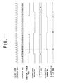
- Fig. 11 shows the case where the relative phase signal of the two-value quantized received signal A is increasingly delayed and the relative phase signal of the two-value quantized received signal B is increasingly advanced.
- the output A of the D flip-flop array 202 increases from seven (7) to nine (9).
- the output B of the D flip-flop array 202 decreases from nine (9) to seven (7). In either case, the output of the D flip-flop array 202 varies in proportion to the variation of the relative phase of the two-value quantized received signal with respect to the virtual phase reference signal.
- the phase detection circuit of Fig. 9 has the following disadvantage.
- the D flip-flop array 202 is driven only at the leading edges of the two-value quantized received signal.
- the relative phase signal output from the phase detection circuit is updated only at each full period of the two-value quantized received signal.
- the value of the relative phase of the two-value quantized received signal can be updated two times for each period of the two-value quantized received signal.
- the phase detection circuit of Fig. 9 has the disadvantage that the rate at which the relative phase signal is updated is low.
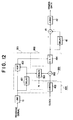
- Fig. 12 is a block diagram of a delayed detection type demodulator provided with a phase detection circuit according to this invention, by which the value of the relative phase of the two-value quantized received signal with respect to the virtual phase reference signal can be updated two times for each period of the two-value quantized received signal.
- the output of limiter amplifier 10 is coupled to a phase detection circuit 400 which includes: a delay element 401 and an exclusive OR element 402 coupled to the limiter amplifier 10; a modulo 2N counter 403 for counting in modulo N, where N is a positive integer; a D flip-flop array 404; and a phase inversion corrector 500.
- the phase inversion corrector 500 includes: a multiplier 501 and an adder 502 for effecting addition in modulo 2N.
- the phase detection circuit 400 is divided into a half-period detector means 901, a phase reference signal generator means 902 and a phase shift determiner means 903.
- the half-period detector means 901 consists of the delay element 401 and the exclusive OR element 402.
- the half-period detector means 901 Upon receiving an input signal of predetermined period from the limiter amplifier 10, the half-period detector means 901 outputs a half-period detection signal at each half-period of the input signal.
- the phase reference signal generator means 902 consists of the modulo 2N counter 403.
- the phase reference signal generator means 902 On the basis of a clock having a frequency not less than twice the frequency of the input signal, the phase reference signal generator means 902 generates the phase reference signal serving as the reference for determining the phase shift of the two-value quantized received signal.
- a phase shift determiner means 903 consists of the D flip-flop array 404 and the phase inversion corrector 500.
- the phase inversion corrector 500 corrects the phase inversion of the phase reference signal at each half-period of the input signal.
- the phase shift determiner means 903 determines and outputs the phase shift of the half-period detection signal relative to the phase reference signal at each half-period of the input signal.
- the delay element 40, subtractor 41, and the judgment circuit 42 are similar to those described above.
- the limiter amplifier 10 shapes the received signal into a rectangular waveform of a constant amplitude. Namely, the limiter amplifier 10 acts as a two-valued quantizer for subjecting the received signal to the two-value quantization, such that the output of the limiter amplifier 10 is quantized to logical "0" and "1".
- the two-value quantized received signal output from the limiter amplifier 10 is supplied to the phase detection circuit 400, where it is first input to the delay element 401.
- the delay time of the delay element 401 is shorter than the half-period of the two-value quantized received signal.
- the delayed received signal output from the delay element 401 is supplied to the exclusive OR element 402, together with the two-value quantized received signal output from the limiter amplifier 10.
- the exclusive OR element 402 effects the logical exclusive OR operation upon the outputs of the limiter amplifier 10 and the delay element 401.
- the output of the exclusive OR element 402 is a pulse signal (referred to as the differential pulse signal) which rises (i.e., has leading edges) at the leading and the tailing edges of the two-value quantized received signal.
- Fig. 13 is a timing chart showing waveforms exemplifying the operation of the delay element 401 and the exclusive OR element 402 of Fig. 12. From top to bottom in Fig. 13 are shown the waveforms of: the two-value quantized received signal; the output of the delay element 401; and the output of the exclusive OR element 402 (the differential pulse signal).
- the delay time of the delay element 401 namely the time length by which the two-value quantized received signal is delayed, is shorter than the half-period of the two-value quantized received signal.
- the differential pulse signal output from the exclusive OR element 402 rises (i.e., has the leading edges) at the leading and the trailing edges of the two-value quantized received signal.
- the modulo 2N counter 403 is driven by a clock having a frequency substantially equal to 2N times the frequency of the two-value quantized received signal. If a virtual phase reference signal similar to that of Fig. 9 is assumed which is obtained by demultiplying the clock signal of the modulo 2N counter 403 by 2N, the virtual phase reference signal rises (i.e., has the leading edge) at the instant when the output of the modulo 2N counter 403 is reset to "0", and falls (i.e., has the trailing edge) at the instant when the output of the modulo 2N counter 403 reaches N. The output of the modulo 2N counter 403 represents the phase of this virtual phase reference signal.
- the output of the modulo 2N counter 403 at each leading edge of the differential pulse signal output from the exclusive OR element 402 represents the phase of the virtual phase reference signal at the leading or the trailing edge of the two-value quantized received signal.
- the absolute phase of the two-value quantized received signal at the trailing edge thereof is equal to 7 r.
- phase shift of the two-value quantized received signal relative to the virtual phase reference signal is given by:
- ⁇ 1 is equal to an integer obtained by first normalizing (i.e., dividing) the time T , between the leading edges of the virtual phase reference signal and the two-value quantized received signal, by the period T of the modulo 2N counter 403 and then discarding the fractional part of the quotient resulting from the division.
- T and ⁇ the following relation holds among ⁇ 1 , T and ⁇ :
- N 8 in the case of Fig. 14
- the output of the modulo 2N counter 403 at a trailing edge of the two-value quantized received signal be represented by ⁇ 2 , where ⁇ 2 E ⁇ 0, 1, ... , 2N-1 ⁇ .
- ⁇ 2 is equal to an integer obtained by: first normalizing (i.e., dividing) the time 7 between the trailing edges of the virtual phase reference signal and the two-value quantized received signal by the period Y of the modulo 2N counter 403; then discarding the fractional part of the quotient resulting from the division; and finally adding numerical value "N" to the quotient.
- the output ⁇ 1 of the modulo 2N counter 403 at the leading edge of the two-value quantized received signal and the value obtained by adding numerical value "N" in modulo 2N to the output ⁇ 2 of the modulo 2N counter 403 at the trailing edge of the two-value quantized received signal can be regarded as representing the relative phase of the two-value quantized received signal with respect to the virtual phase reference signal.
- the relative phase of the two-value quantized received signal can be obtained by correcting the output of the modulo 2N counter 403, i.e., by adding the numerical value "0" at the leading edge, and the numerical value "N" at the trailing edge, of the two-value quantized received signal.
- the phase inversion corrector 500 effects this correction for the output of the modulo 2N counter 403. Namely, upon receiving the output of the modulo 2N counter 403, the phase inversion corrector 500 adds to it the numerical value "0" at the leading edge, and the numerical value "N" at the trailing edge, of the two-value quantized received signal. Next, the operation of the phase inversion corrector 500 is described by reference to drawings.
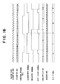
- Fig. 16 is a view similar to that of Fig. 15, but showing the case where the relative phase of the two-value quantized received signal with respect to the virtual phase reference signal is increasingly delayed.
- Fig. 17 is a view similar to that of Fig. 15, but showing the case where the relative phase of the two-value quantized received signal with respect to the virtual phase reference signal is increasingly advanced.
- the value of the delayed received signal output from the delay element 401 is at logical "0" at the leading edge, and at logical “1" " at the trailing edge, of the two-value quantized received signal.
- the multiplier 501 multiplies output of the delay element 401 by N, thereby outputting the numerical value "0" at the leading edge, and the numerical value "N” at the trailing edge, of the two-value quantized received signal.
- the adder 502 adds in modulo 2N the outputs of the modulo 2N counter 403 and the multiplier 501, thereby obtaining the output of the phase inversion corrector 500.
- the output of the phase inversion corrector 500 is equal to the output of the modulo 2N counter 403 at the leading edge of the two-value quantized received signal.
- the output of the phase inversion corrector 500 is equal to the value obtained by adding in modulo 2N the numerical value "N" to the output of the modulo 2N counter 403, at the trailing edge of the two-value quantized received signal.
- the output of the phase inversion corrector 500 is supplied to the D flip-flop array 404, which is driven (i.e., reset) by the differential pulse signal output from the exclusive OR element 402.
- the differential pulse signal has leading edges at the leading and trailing edges of the two-value quantized received signal.
- the D flip-flop array 404 is reset at each leading and trailing edge of the two-value quantized received signal.
- ⁇ the output of the D flip-flop array 404 is represented by ⁇ , then 11. is expressed in terms of the output values ⁇ 1 and Q 2 of the modulo 2N counter 403 at the leading and the trailing edges, respectively:
- the output of the D flip-flop array 202 representing the relative phase of the two-value quantized received signal is updated only once for each period of the two-value quantized received signal.
- the D flip-flop array 404 is driven by the differential pulse signal at the leading and the trailing edges of the two-value quantized received signal.
- the output of the D flip-flop array 404 representing the relative phase of the two-value quantized received signal is updated twice for each period of the two-value quantized received signal.
- the updating rate of the relative phase signal is thereby doubled. This can be easily comprehended by comparing Fig. 15 with Fig. 10 and Figs. 16 and 17 with Fig. 11.
- the two-value quantized received signal A of Fig. 11 and the two-value quantized received signal of Fig. 16 are the same.
- the output A of the D flip-flop array 202 in Fig. 11 varies from “7” to “9”, while the output of the D flip-flop array 404 in Fig. 16 varies gradually from “7” to "8” to "9”.
- the two-value quantized received signal B of Fig. 11 and the two-value quantized received signal of Fig. 17 are the same.
- the output B of the D flip-flop array 202 in Fig. 11 varies from "9” to "7”
- the output of the D flip-flop array 404 in Fig. 17 varies gradually from “9” to "8” to "7”.
- the updating rate of the relative phase signal is doubled for the circuit of Fig. 12, and hence the variation of the value of the relative phase signal is rendered less abrupt.
- the phase inversion corrector 500 consists of the multiplier 501 and the adder 502.
- the element corresponding to the multiplier 501 may be implemented by any circuit which outputs numerical value "0" upon receiving numerical value "0", and numerical value "N” upon receiving numerical value "1".
- Such element may be implemented by a data selector which selects and outputs numerical value "0” upon receiving numerical value "0", and numerical value "N” upon receiving numerical value "1”.
- the phase inversion corrector 500 may consist of logical product elements (AND gates) for effecting logical product operations (AND operations) upon the respective bits of the numerical value "N" and the output of the delay element 401.
- the above description relates to the case where the received signal is modulated in accordance with the differential phase shift keying (DPSK).
- DPSK differential phase shift keying
- the constant N may be any positive integer.
- Fig. 18 is a block diagram of another delayed detection type demodulator provided with a phase detection circuit according to this invention, by which the value of the relative phase of the two-value quantized received signal with respect to the virtual phase reference signal can be updated two times for each period of the two-value quantized received signal.
- the phase detection circuit 400a is functionally divided into: a half-period detector means 901 consisting of the delay element 401 and the exclusive OR element 402; a phase reference signal generator means 902 consisting of the modulo 2M counter 403a, where M is a positive integer; and a phase shift determiner means 903 consisting of the D flip-flop array 404a and a phase inversion corrector 500a.
- the phase inversion corrector 500a consists of an exclusive OR element 503 having inputs coupled to the output of the delay element 401 and the most significant bit (MSB) of the output of the modulo 2M counter 403a.
- the combination of the least significant bits (namely the first through (M- I)th bit of the modulo 2M counter 403a) and the output of the exclusive OR element 503 is input to the D flip-flop array 404a. Otherwise the circuit of Fig. 18 is similar to the circuit of Fig. 12.
- the limiter amplifier 10 shapes the received signal into a rectangular waveform of a constant amplitude. Namely, the limiter amplifier 10 acts as a two-valued quantizer for subjecting the received signal to the two-value quantization, such that the output of the limiter amplifier 10 is quantized to logical "0" and "1".
- the two-value quantized received signal output from the limiter amplifier 10 is supplied to the phase detection circuit 400a, where it is first input to the delay element 401 and the exclusive OR element 402.
- the delay time of the delay element 401 is shorter than the half-period of the two-value quantized received signal.
- the delayed received signal output from the delay element 401 is supplied to-the exclusive OR element 402.
- the exclusive OR element 402 effects the logical exclusive OR operation upon the outputs of the limiter amplifier 10 and the delay element 401.
- the output of the exclusive OR element 402 is a pulse signal (referred to as the differential pulse signal) which rises (i.e., has leading edges) at the leading and the tailing edges of the two-value quantized received signal.
- the modulo 2M counter 403a is driven by a clock having a frequency substantially equal to 2 m times the frequency of the two-value quantized received signal, where M is a positive integer. If a virtual phase reference signal similar to that of Fig. 9 is assumed which is obtained by demultiplying the clock signal of the modulo 2 M counted 403a by 2M, the virtual phase reference signal rises (i.e., has the leading edge) at the instant when the output of the modulo 2 M counter 403a is reset to "0", and falls (i.e., has the trailing edge) at the instant when the output of the modulo 2 M counter 403a reaches 2 M-1 . The output of the modulo 2 M counter 403a represents the phase of this virtual phase reference signal.
- the output of the modulo 2 M counter 403a at each leading edge of the differential pulse signal output from the exclusive OR element 402 represents the phase of the virtual phase reference signal at the leading or the trailing edge of the two-value quantized received signal.
- the absolute phase of the two-value quantized received signal at the trailing edge thereof is equal to ⁇ .
- the phase inversion corrector 500a effects this correction for the output of the modulo 2 M counter 403a. Namely, upon receiving the output of the modulo 2 M counter 403a, the phase inversion corrector 500a adds to it the numerical value "0" at the leading edge, and the numerical value "2 M-1 " at the trailing edge, of the two-value quantized received signal. Next, the operation of the phase inversion corrector 500a is described by reference to drawings.
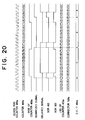
- Fig. 20 is a view similar to that of Fig. 19, but showing the case where the relative phase of the two-value quantized received signal with respect to the virtual phase reference signal is increasingly delayed.
- Fig. 21 is a view similar to that of Fig. 19, but showing the case where the relative phase of the two-value quantized received signal with respect to the virtual phase reference signal is increasingly advanced.
- the numbers at the waveforms of the modulo 2 M counter 403a, the least significant bits of the 403a, the phase inversion corrector 500a, and the D flip-flop array 404a represent the values thereof
- the output of the modulo 2 M counter 403a consists of M bits.
- the most significant bit of the modulo 2 M counter 403a represents the the numerical value 2 M-1 .
- adding the numerical value 2 M-1 to the output of the modulo 2 M counter 403a in modulo 2M is equivalent to logical inversion of the most significant bit of the modulo 2 M counter 403a.
- adding numerical value "0" and "1 ", respectively, to the output of the modulo 2 M counter 403a at the leading and the trailing edges of the two-value quantized received signal results in effecting no logical inversion at the leading edge, and the logical inversion at the trailing edge, of the two-value quantized received signal, upon the most significant bit of the modulo 2 M counter 403a.
- the value of the delayed received signal output from the delay element 401 is at logical "0" at the leading edge, and at logical "1" " at the trailing edge, of the two-value quantized received signal.
- the exclusive OR element 503 effects the logical exclusive OR operation upon the delayed received signal output from the delay element 401 and the most significant bit of the output from the modulo 2 M counter 403a.
- the output of the 503 is combined as the new most significant bit with the least significant bits (the first through (M - 1)th bits) of the modulo 2 M counter 403a, to form the output of the phase inversion corrector 500a.
- the output of the phase inversion corrector 500a is equal to the output of the modulo 2 M counter 403a at the leading edges of the two-value quantized received signal (no logical inversion of the most significant bit is effected).
- the output of the phase inversion corrector 500a at the trailing edges of the two-value quantized received signal consists of the logically inverted most significant bit of the modulo 2 M counter 403a combined with the least significant bits thereof.
- the output of the phase inversion corrector 500a is equal to the value obtained by adding numerical value "0" at the leading edge, and numerical value "2 M-1 " at the trailing edge, of the two-value quantized received signal, to the output of the modulo 2 M counter 403a.
- the phase inversion corrector 500a can be implemented only by the exclusive OR element 503.
- the circuit of Fig. 18 is simplified compared to the circuit of Fig. 12.
- the output of the phase inversion corrector 500a is supplied to the D flip-flop array 404a, which is driven (i.e., reset) by the differential pulse signal output from the exclusive OR element 402.
- the differential pulse signal has leading edges at the leading and trailing edges of the two-value quantized received signal.
- the D flip-flop array 404a is reset at each leading and trailing edge of the two-value quantized received signal.
- ⁇ is expressed in terms of the output values ⁇ 1 and ⁇ 2 ( ⁇ 1 , ⁇ 2 E ⁇ 0, 1, ... , 2 M - 11) of the modulo 2 M counter 403a at the leading and the trailing edges, respectively:
- the D flip-flop array 404a of Fig. 18 is driven by the differential pulse signal at the leading and the trailing edges of the two-value quantized received signal
- the output of the D flip-flop array 404a representing the relative phase of the two-value quantized received signal is updated twice for each period of the two-value quantized received signal.
- the updating rate of the relative phase signal is thereby doubled compared to the case of Fig. 9. This can be easily comprehended by comparing Fig. 19 with Fig. 10 and Figs. 20 and 21 with Fig. 11.
- the two-value quantized received signal A of Fig. 11 and the two-value quantized received signal of Fig. 20 are the same.
- the output A of the D flip-flop array 202 in Fig. 11 varies from “7” to “9”, while the output of the D flip-flop array 404a in Fig. 20 varies gradually from “7” to "8” to “9”.
- the two-value quantized received signal B of Fig. 11 and the two-value quantized received signal of Fig. 21 are the same.
- the output B of the D flip-flop array 202 in Fig. 11 varies from “9” to "7”
- the output of the D flip-flop array 404a in Fig. 21 varies gradually from “9” to "8” to "7”.
- the updating rate of the relative phase signal is doubled for the circuit of Fig. 12, and hence the variation of the value of the relative phase signal is rendered less abrupt.
- the above description relates to the case where the received signal is modulated in accordance with the differential phase shift keying (DPSK).
- DPSK differential phase shift keying
- the principle embodied in the circuit of Fig. 18 can be applied to MSK or GMSK modulation systems.
- the constant M may be any positive integer.
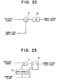
- Fig. 22 recapitulates the frequency converter 20 of Fig. 8.
- the received signal having a frequency f 1 Hz is multiplied by the signal for frequency conversion (the frequency conversion signal) having a frequency f 2 Hz, where:
- the output of the multiplier 21 includes frequency components at f 1 + f 2 Hz and
- the output of the multiplier 21 is supplied to the low pass filter 22.
- the low pass filter 22 passes only the low frequency component at
- the low pass filter 22 outputs a signal at
- f 1 - f 2 Hz of the converted signal output from the low pass filter 22 is less than the frequency f 1 Hz of the received signal.
- the frequency converter of Fig. 22 uses a low pass filter 22 for removing the high frequency components.
- the low pass filter 22 generally has a complicated structure and tends to be large- sized and consumes power.
- Fig. 23 is a block diagram showing an alternate structure of the frequency converter according to this invention.
- the output of the exclusive OR element 71 functioning as a multiplier and having an input for the received signal is coupled to the D-input of a D flip-flop 72 serving as a sampler.
- the sampling clock driving the D flip-flop 72 is demultiplied by two by a frequency demultiplier 73 and thence supplied to the other input of the exclusive OR element 71.
- the frequency demultiplier 73 demultiplies the sampling clock by two and outputs the demultiplied clock signal to the exclusive OR element 71 as the signal for frequency conversion (the frequency conversion signal). Namely, if the frequency of the sampling clock is represented by f, Hz, then the frequency of the frequency conversion signal is f s /2 Hz.
- the received signal input to the exclusive OR element 71 is a two-valued digital signal taking either the logical "0" or logical "1". As in the case of the circuit of Fig. 22, the following relation holds between the frequency f 1 Hz of the received signal and the frequency f s /2 of the frequency conversion signal:
- the exclusive OR element 71 effects the logical exclusive OR operation upon the received signal and the output of the frequency demultiplier 73, both of which are logical two-valued signals. If the logical "0" and the logical "1" are converted into the numerical values " 1" and "- 1", respectively, the logical exclusive OR operation is converted to the multiplication operation of the numerical values.
- the exclusive OR element 71 acts as a multiplier for multiplying the received signal by the frequency conversion signal output from the frequency demultiplier 73.
- the output of the exclusive OR element 71 is a multiplication of the received signal at frequency f 1 Hz by the frequency conversion signal at frequency f s /2 Hz. Consequently, the output of the exclusive OR element 51 includes components at frequency f 1 + f s /2 Hz and
- the output of the exclusive OR element 71 is supplied to the D flip-flop 72. Since the D flip-flop 72 is driven by the sampling clock at frequency f s Hz, the D flip-flop 72 samples the output off the exclusive OR element 51 at f s Hz. It is assumed here that:
- a signal at a frequency F Hz is input to the D flip-flop 72, where the frequency F Hz satisfies the relation: f s /2 ⁇ F ⁇ 3 f s /2, as does the high frequency component at f 1 + f s /2 Hz of the output of the exclusive OR element 71, then, the signal is sampled at f s Hz, or the frequency of the sampling clock driving the D flip-flop 72. Under this circumstance, the signal at a frequency higher than the Nyquist frequency of sampling is sampled. As a result, the aliasing phenomenon is observed, and a frequency component at
- the aliasing phenomenon is discussed, for example, in: M. Hino, "SPECTRAL ANALYSIS,” pp. 175 through 177, Asakura Shoten, 1977.
- the high frequency component of the output of the exclusive OR element 71 namely the component at f 1 + f s /2 Hz, appears as the frequency component at
- Hz of the output of the exclusive OR element 71 appear as the frequency component at
- the D flip-flop 72 outputs a signal consisting solely of the frequency component at
- f 1 f s /2 Hz of the output of the D flip-flop 72 is less than the frequency f 1 Hz of the received signal.
- the low pass filter of the conventional circuit of Fig. 22 can thus be dispensed with. Since the size and power consumption of a D flip-flop is smaller than those of a low pass filter, the overall size and power consumption can be reduced.
Landscapes
- Engineering & Computer Science (AREA)
- Power Engineering (AREA)
- Computer Networks & Wireless Communication (AREA)
- Signal Processing (AREA)
- Digital Transmission Methods That Use Modulated Carrier Waves (AREA)
- Manipulation Of Pulses (AREA)
Priority Applications (2)
| Application Number | Priority Date | Filing Date | Title |
|---|---|---|---|
| EP97120802A EP0833483A3 (fr) | 1991-12-27 | 1992-12-24 | Dispositif comparateur de phase pour démodulateur utilisant une détection différentielle |
| EP97120803A EP0831625A3 (fr) | 1991-12-27 | 1992-12-24 | Circuit de détection de phase et démodulateur utilisant une détection différentielle |
Applications Claiming Priority (6)
| Application Number | Priority Date | Filing Date | Title |
|---|---|---|---|
| JP3347245A JP2837982B2 (ja) | 1991-12-27 | 1991-12-27 | 遅延検波復調装置 |
| JP347245/91 | 1991-12-27 | ||
| JP4053583A JP2932820B2 (ja) | 1992-03-12 | 1992-03-12 | 位相検波回路及び遅延検波復調装置及び位相検波方法 |
| JP53583/92 | 1992-03-12 | ||
| JP6712492A JPH05276061A (ja) | 1992-03-25 | 1992-03-25 | 周波数変換回路 |
| JP67124/92 | 1992-03-25 |
Related Child Applications (2)
| Application Number | Title | Priority Date | Filing Date |
|---|---|---|---|
| EP97120803A Division EP0831625A3 (fr) | 1991-12-27 | 1992-12-24 | Circuit de détection de phase et démodulateur utilisant une détection différentielle |
| EP97120802A Division EP0833483A3 (fr) | 1991-12-27 | 1992-12-24 | Dispositif comparateur de phase pour démodulateur utilisant une détection différentielle |
Publications (3)
| Publication Number | Publication Date |
|---|---|
| EP0548982A2 true EP0548982A2 (fr) | 1993-06-30 |
| EP0548982A3 EP0548982A3 (fr) | 1994-04-13 |
| EP0548982B1 EP0548982B1 (fr) | 1999-04-07 |
Family
ID=27295001
Family Applications (3)
| Application Number | Title | Priority Date | Filing Date |
|---|---|---|---|
| EP97120802A Withdrawn EP0833483A3 (fr) | 1991-12-27 | 1992-12-24 | Dispositif comparateur de phase pour démodulateur utilisant une détection différentielle |
| EP92121972A Expired - Lifetime EP0548982B1 (fr) | 1991-12-27 | 1992-12-24 | Circuit de conversion de fréquence |
| EP97120803A Withdrawn EP0831625A3 (fr) | 1991-12-27 | 1992-12-24 | Circuit de détection de phase et démodulateur utilisant une détection différentielle |
Family Applications Before (1)
| Application Number | Title | Priority Date | Filing Date |
|---|---|---|---|
| EP97120802A Withdrawn EP0833483A3 (fr) | 1991-12-27 | 1992-12-24 | Dispositif comparateur de phase pour démodulateur utilisant une détection différentielle |
Family Applications After (1)
| Application Number | Title | Priority Date | Filing Date |
|---|---|---|---|
| EP97120803A Withdrawn EP0831625A3 (fr) | 1991-12-27 | 1992-12-24 | Circuit de détection de phase et démodulateur utilisant une détection différentielle |
Country Status (7)
| Country | Link |
|---|---|
| US (3) | US5313170A (fr) |
| EP (3) | EP0833483A3 (fr) |
| AU (2) | AU653660B2 (fr) |
| CA (1) | CA2086279C (fr) |
| DE (1) | DE69228862T2 (fr) |
| FI (1) | FI925870A7 (fr) |
| NO (1) | NO925012L (fr) |
Families Citing this family (16)
| Publication number | Priority date | Publication date | Assignee | Title |
|---|---|---|---|---|
| JP2837982B2 (ja) * | 1991-12-27 | 1998-12-16 | 三菱電機株式会社 | 遅延検波復調装置 |
| US5406218A (en) * | 1993-02-19 | 1995-04-11 | Hitachi, Ltd. | Phase demodulator receiving inputs from phase detector and binary phase detector |
| IL107656A (en) * | 1993-11-18 | 1996-11-14 | Dsp Telecomm Ltd | Demodulator |
| US5539776A (en) * | 1993-11-24 | 1996-07-23 | At&T Corp. | All digital if-to-baseband signal converter |
| US5757868A (en) * | 1994-02-16 | 1998-05-26 | Motorola, Inc. | Digital phase detector with integrated phase detection |
| US5572588A (en) * | 1994-07-05 | 1996-11-05 | Motorola, Inc. | Method and apparatus for detecting reception of a tone signal |
| JP3390272B2 (ja) * | 1994-11-10 | 2003-03-24 | 沖電気工業株式会社 | 同期検波回路 |
| CN1087120C (zh) * | 1994-11-10 | 2002-07-03 | 松下电器产业株式会社 | 直接变频接收机 |
| EP0800284B1 (fr) * | 1996-04-04 | 2006-01-04 | New Japan Radio Corp., Ltd. | Corrélateur pour des signaux à spectre étalé |
| JPH1093646A (ja) * | 1996-09-12 | 1998-04-10 | Pacific Commun Res:Kk | ディジタル直交検波回路 |
| US6026117A (en) | 1997-10-23 | 2000-02-15 | Interdigital Technology Corporation | Method and apparatus for generating complex four-phase sequences for a CDMA communication system |
| US6160434A (en) * | 1998-05-14 | 2000-12-12 | Mitsubishi Denki Kabushiki Kaisha | Ninety-degree phase shifter |
| DE10017923C2 (de) * | 2000-04-11 | 2003-01-02 | Siemens Ag | Messanordnung mit zwei phasenselektiven Gleichrichtern |
| US6969984B2 (en) * | 2000-12-21 | 2005-11-29 | Tropian, Inc. | Direct phase and frequency demodulation |
| US7164731B2 (en) * | 2003-03-31 | 2007-01-16 | Via Technologies, Inc. | Apparatus and method of adaptive frequency offset estimations for a receiver |
| US8218644B1 (en) | 2009-05-12 | 2012-07-10 | Accumulus Technologies Inc. | System for compressing and de-compressing data used in video processing |
Family Cites Families (9)
| Publication number | Priority date | Publication date | Assignee | Title |
|---|---|---|---|---|
| GB1178935A (en) * | 1967-09-13 | 1970-01-21 | Philips Electronic Associated | Low-Frequency Generator |
| US4190802A (en) * | 1978-08-17 | 1980-02-26 | Motorola, Inc. | Digital demodulator for phase shift keyed signals |
| US4804925A (en) * | 1986-03-26 | 1989-02-14 | Fuji Photo Film Co., Ltd. | DPSK exclusive-OR demodulator |
| JP2554705B2 (ja) * | 1988-04-25 | 1996-11-13 | 三菱電機株式会社 | 位相同期回路 |
| US4878029A (en) * | 1988-12-05 | 1989-10-31 | General Electric Company | Complex digital sampling converter for demodulator |
| FR2644952A1 (fr) * | 1989-03-21 | 1990-09-28 | Duranton Rene | Modulateur-demodulateur de phase utilisant des portes " ou exclusif " |
| EP0434355A3 (en) * | 1989-12-18 | 1993-02-24 | Nec Corporation | Differential phase demodulator for psk-modulated signals |
| JPH03274844A (ja) * | 1990-03-24 | 1991-12-05 | Japan Radio Co Ltd | Psk変調信号の遅延検波回路 |
| JP2771354B2 (ja) * | 1991-08-26 | 1998-07-02 | 日本電気株式会社 | 復調器 |
-
1992
- 1992-12-23 FI FI925870A patent/FI925870A7/fi unknown
- 1992-12-23 NO NO92925012A patent/NO925012L/no not_active Application Discontinuation
- 1992-12-24 EP EP97120802A patent/EP0833483A3/fr not_active Withdrawn
- 1992-12-24 DE DE69228862T patent/DE69228862T2/de not_active Expired - Fee Related
- 1992-12-24 EP EP92121972A patent/EP0548982B1/fr not_active Expired - Lifetime
- 1992-12-24 AU AU30425/92A patent/AU653660B2/en not_active Ceased
- 1992-12-24 CA CA002086279A patent/CA2086279C/fr not_active Expired - Fee Related
- 1992-12-24 EP EP97120803A patent/EP0831625A3/fr not_active Withdrawn
- 1992-12-24 US US07/997,768 patent/US5313170A/en not_active Expired - Lifetime
-
1994
- 1994-03-28 US US08/218,977 patent/US5485108A/en not_active Expired - Lifetime
- 1994-03-28 US US08/219,020 patent/US5369374A/en not_active Expired - Lifetime
- 1994-07-25 AU AU68690/94A patent/AU660878B2/en not_active Ceased
Also Published As
| Publication number | Publication date |
|---|---|
| US5485108A (en) | 1996-01-16 |
| EP0831625A3 (fr) | 2006-08-16 |
| AU660877B2 (en) | 1995-07-06 |
| EP0831625A2 (fr) | 1998-03-25 |
| AU660878B2 (en) | 1995-07-06 |
| EP0833483A3 (fr) | 2006-08-16 |
| US5369374A (en) | 1994-11-29 |
| AU3042592A (en) | 1993-07-01 |
| CA2086279A1 (fr) | 1993-06-28 |
| DE69228862T2 (de) | 1999-10-07 |
| NO925012L (no) | 1993-06-28 |
| CA2086279C (fr) | 1999-08-10 |
| FI925870A0 (fi) | 1992-12-23 |
| NO925012D0 (no) | 1992-12-23 |
| EP0833483A2 (fr) | 1998-04-01 |
| AU653660B2 (en) | 1994-10-06 |
| US5313170A (en) | 1994-05-17 |
| EP0548982B1 (fr) | 1999-04-07 |
| DE69228862D1 (de) | 1999-05-12 |
| AU6868894A (en) | 1994-09-22 |
| AU6869094A (en) | 1994-09-22 |
| FI925870A7 (fi) | 1993-06-28 |
| EP0548982A3 (fr) | 1994-04-13 |
Similar Documents
| Publication | Publication Date | Title |
|---|---|---|
| US5122758A (en) | Differential phase demodulator for psk-modulated signals | |
| CA2086279C (fr) | Demodulateur a detection retardee | |
| EP0978972A2 (fr) | Récupération d'horloge pour un démodulateur | |
| US5535252A (en) | Clock synchronization circuit and clock synchronizing method in baseband demodulator of digital modulation type | |
| EP0464814A2 (fr) | Démodulateur PSK non cohérent | |
| US5640427A (en) | Demodulator | |
| US5484987A (en) | Delayed detection type demodulator | |
| EP0771097B1 (fr) | Détecteur différentiel pour signaux MDP | |
| EP0783206A2 (fr) | Détecteur de verrouillage d'un circuit de synchronisation de données et méthode de fonctionnement correspondante | |
| US6359942B1 (en) | FSK demodulator | |
| EP0198701B1 (fr) | Circuit de détection de phase | |
| GB2234411A (en) | Integrated circuit for digital demodulation | |
| EP0783214A2 (fr) | Détecteur de phase d'un synchronisateur de données et méthode et l'opération de celui | |
| EP0234900B1 (fr) | Circuit détecteur de phase | |
| CA2204046C (fr) | Demodulateur de detection differentiel et comparateur de phase connexe | |
| US6163209A (en) | Demodulation of angle modulated carriers using a noncoherent reference | |
| US20100254491A1 (en) | Dc offset compensating system and method | |
| JP2504243B2 (ja) | 復調方式 | |
| JP3237322B2 (ja) | Cn比測定手段 | |
| JP2004343166A (ja) | Ask復調回路 | |
| JP3260691B2 (ja) | ユニークワード検出回路 | |
| JP3183456B2 (ja) | クロック再生回路及びこれを用いた受信装置 | |
| JP2744542B2 (ja) | デジタル信号受信装置 | |
| JP2744541B2 (ja) | 二重差動符号化通信装置 | |
| JPH0993292A (ja) | 4値fsk検波回路 |
Legal Events
| Date | Code | Title | Description |
|---|---|---|---|
| PUAI | Public reference made under article 153(3) epc to a published international application that has entered the european phase |
Free format text: ORIGINAL CODE: 0009012 |
|
| AK | Designated contracting states |
Kind code of ref document: A2 Designated state(s): DE FR GB IT SE |
|
| PUAL | Search report despatched |
Free format text: ORIGINAL CODE: 0009013 |
|
| AK | Designated contracting states |
Kind code of ref document: A3 Designated state(s): DE FR GB IT SE |
|
| 17P | Request for examination filed |
Effective date: 19940905 |
|
| 17Q | First examination report despatched |
Effective date: 19970624 |
|
| GRAG | Despatch of communication of intention to grant |
Free format text: ORIGINAL CODE: EPIDOS AGRA |
|
| GRAG | Despatch of communication of intention to grant |
Free format text: ORIGINAL CODE: EPIDOS AGRA |
|
| GRAH | Despatch of communication of intention to grant a patent |
Free format text: ORIGINAL CODE: EPIDOS IGRA |
|
| GRAH | Despatch of communication of intention to grant a patent |
Free format text: ORIGINAL CODE: EPIDOS IGRA |
|
| GRAA | (expected) grant |
Free format text: ORIGINAL CODE: 0009210 |
|
| AK | Designated contracting states |
Kind code of ref document: B1 Designated state(s): DE FR GB IT SE |
|
| ET | Fr: translation filed | ||
| REF | Corresponds to: |
Ref document number: 69228862 Country of ref document: DE Date of ref document: 19990512 |
|
| PLBE | No opposition filed within time limit |
Free format text: ORIGINAL CODE: 0009261 |
|
| STAA | Information on the status of an ep patent application or granted ep patent |
Free format text: STATUS: NO OPPOSITION FILED WITHIN TIME LIMIT |
|
| 26N | No opposition filed | ||
| REG | Reference to a national code |
Ref country code: GB Ref legal event code: 746 Effective date: 20010103 |
|
| REG | Reference to a national code |
Ref country code: FR Ref legal event code: D6 |
|
| REG | Reference to a national code |
Ref country code: GB Ref legal event code: IF02 |
|
| PGFP | Annual fee paid to national office [announced via postgrant information from national office to epo] |
Ref country code: SE Payment date: 20041206 Year of fee payment: 13 |
|
| PGFP | Annual fee paid to national office [announced via postgrant information from national office to epo] |
Ref country code: FR Payment date: 20041208 Year of fee payment: 13 |
|
| PGFP | Annual fee paid to national office [announced via postgrant information from national office to epo] |
Ref country code: DE Payment date: 20041216 Year of fee payment: 13 |
|
| PGFP | Annual fee paid to national office [announced via postgrant information from national office to epo] |
Ref country code: GB Payment date: 20041222 Year of fee payment: 13 |
|
| PG25 | Lapsed in a contracting state [announced via postgrant information from national office to epo] |
Ref country code: IT Free format text: LAPSE BECAUSE OF NON-PAYMENT OF DUE FEES;WARNING: LAPSES OF ITALIAN PATENTS WITH EFFECTIVE DATE BEFORE 2007 MAY HAVE OCCURRED AT ANY TIME BEFORE 2007. THE CORRECT EFFECTIVE DATE MAY BE DIFFERENT FROM THE ONE RECORDED. Effective date: 20051224 Ref country code: GB Free format text: LAPSE BECAUSE OF NON-PAYMENT OF DUE FEES Effective date: 20051224 |
|
| PG25 | Lapsed in a contracting state [announced via postgrant information from national office to epo] |
Ref country code: SE Free format text: LAPSE BECAUSE OF NON-PAYMENT OF DUE FEES Effective date: 20051225 |
|
| PG25 | Lapsed in a contracting state [announced via postgrant information from national office to epo] |
Ref country code: DE Free format text: LAPSE BECAUSE OF NON-PAYMENT OF DUE FEES Effective date: 20060701 |
|
| EUG | Se: european patent has lapsed | ||
| GBPC | Gb: european patent ceased through non-payment of renewal fee |
Effective date: 20051224 |
|
| PG25 | Lapsed in a contracting state [announced via postgrant information from national office to epo] |
Ref country code: FR Free format text: LAPSE BECAUSE OF NON-PAYMENT OF DUE FEES Effective date: 20060831 |
|
| REG | Reference to a national code |
Ref country code: FR Ref legal event code: ST Effective date: 20060831 |