EP0549845A1 - System für integrierter Lochfeststellung im Band - Google Patents
System für integrierter Lochfeststellung im Band Download PDFInfo
- Publication number
- EP0549845A1 EP0549845A1 EP92105131A EP92105131A EP0549845A1 EP 0549845 A1 EP0549845 A1 EP 0549845A1 EP 92105131 A EP92105131 A EP 92105131A EP 92105131 A EP92105131 A EP 92105131A EP 0549845 A1 EP0549845 A1 EP 0549845A1
- Authority
- EP
- European Patent Office
- Prior art keywords
- tape
- hole
- pattern
- areas
- edge
- Prior art date
- Legal status (The legal status is an assumption and is not a legal conclusion. Google has not performed a legal analysis and makes no representation as to the accuracy of the status listed.)
- Granted
Links
- 238000001514 detection method Methods 0.000 title claims abstract description 13
- 238000000034 method Methods 0.000 claims abstract description 16
- 239000011159 matrix material Substances 0.000 claims description 6
- 238000012360 testing method Methods 0.000 claims description 6
- 238000004519 manufacturing process Methods 0.000 claims description 4
- 238000012545 processing Methods 0.000 claims description 3
- 238000005286 illumination Methods 0.000 claims description 2
- 230000007704 transition Effects 0.000 claims 2
- 230000003287 optical effect Effects 0.000 abstract description 4
- 230000008569 process Effects 0.000 description 4
- 230000001360 synchronised effect Effects 0.000 description 4
- 238000010586 diagram Methods 0.000 description 3
- 230000006870 function Effects 0.000 description 2
- 238000012986 modification Methods 0.000 description 2
- 230000004048 modification Effects 0.000 description 2
- 230000010363 phase shift Effects 0.000 description 2
- 230000003068 static effect Effects 0.000 description 2
- 239000000758 substrate Substances 0.000 description 2
- 238000012935 Averaging Methods 0.000 description 1
- 102100040856 Dual specificity protein kinase CLK3 Human genes 0.000 description 1
- 102100040858 Dual specificity protein kinase CLK4 Human genes 0.000 description 1
- 101000749304 Homo sapiens Dual specificity protein kinase CLK3 Proteins 0.000 description 1
- 101000749298 Homo sapiens Dual specificity protein kinase CLK4 Proteins 0.000 description 1
- WYTGDNHDOZPMIW-RCBQFDQVSA-N alstonine Natural products C1=CC2=C3C=CC=CC3=NC2=C2N1C[C@H]1[C@H](C)OC=C(C(=O)OC)[C@H]1C2 WYTGDNHDOZPMIW-RCBQFDQVSA-N 0.000 description 1
- 230000003466 anti-cipated effect Effects 0.000 description 1
- 230000006835 compression Effects 0.000 description 1
- 238000007906 compression Methods 0.000 description 1
- 230000001934 delay Effects 0.000 description 1
- 238000013461 design Methods 0.000 description 1
- 238000003708 edge detection Methods 0.000 description 1
- 238000005516 engineering process Methods 0.000 description 1
- 238000001914 filtration Methods 0.000 description 1
- 238000007689 inspection Methods 0.000 description 1
- 230000010354 integration Effects 0.000 description 1
- 239000000463 material Substances 0.000 description 1
- 239000002184 metal Substances 0.000 description 1
- 238000001465 metallisation Methods 0.000 description 1
- 230000000149 penetrating effect Effects 0.000 description 1
- 230000004044 response Effects 0.000 description 1
- 230000011664 signaling Effects 0.000 description 1
- 230000001629 suppression Effects 0.000 description 1
- 230000002123 temporal effect Effects 0.000 description 1
- 238000012546 transfer Methods 0.000 description 1
Images
Classifications
-
- G—PHYSICS
- G11—INFORMATION STORAGE
- G11B—INFORMATION STORAGE BASED ON RELATIVE MOVEMENT BETWEEN RECORD CARRIER AND TRANSDUCER
- G11B15/00—Driving, starting or stopping record carriers of filamentary or web form; Driving both such record carriers and heads; Guiding such record carriers or containers therefor; Control thereof; Control of operating function
- G11B15/02—Control of operating function, e.g. switching from recording to reproducing
- G11B15/05—Control of operating function, e.g. switching from recording to reproducing by sensing features present on or derived from record carrier or container
- G11B15/06—Control of operating function, e.g. switching from recording to reproducing by sensing features present on or derived from record carrier or container by sensing auxiliary features on record carriers or containers, e.g. to stop machine near the end of a tape
- G11B15/08—Control of operating function, e.g. switching from recording to reproducing by sensing features present on or derived from record carrier or container by sensing auxiliary features on record carriers or containers, e.g. to stop machine near the end of a tape by photoelectric sensing
-
- G—PHYSICS
- G11—INFORMATION STORAGE
- G11B—INFORMATION STORAGE BASED ON RELATIVE MOVEMENT BETWEEN RECORD CARRIER AND TRANSDUCER
- G11B23/00—Record carriers not specific to the method of recording or reproducing; Accessories, e.g. containers, specially adapted for co-operation with the recording or reproducing apparatus ; Intermediate mediums; Apparatus or processes specially adapted for their manufacture
- G11B23/38—Visual features other than those contained in record tracks or represented by sprocket holes the visual signals being auxiliary signals
-
- G—PHYSICS
- G11—INFORMATION STORAGE
- G11B—INFORMATION STORAGE BASED ON RELATIVE MOVEMENT BETWEEN RECORD CARRIER AND TRANSDUCER
- G11B27/00—Editing; Indexing; Addressing; Timing or synchronising; Monitoring; Measuring tape travel
- G11B27/10—Indexing; Addressing; Timing or synchronising; Measuring tape travel
- G11B27/19—Indexing; Addressing; Timing or synchronising; Measuring tape travel by using information detectable on the record carrier
- G11B27/24—Indexing; Addressing; Timing or synchronising; Measuring tape travel by using information detectable on the record carrier by sensing features on the record carrier other than the transducing track ; sensing signals or marks recorded by another method than the main recording
- G11B27/26—Indexing; Addressing; Timing or synchronising; Measuring tape travel by using information detectable on the record carrier by sensing features on the record carrier other than the transducing track ; sensing signals or marks recorded by another method than the main recording by photoelectric detection, e.g. of sprocket holes
-
- G—PHYSICS
- G11—INFORMATION STORAGE
- G11B—INFORMATION STORAGE BASED ON RELATIVE MOVEMENT BETWEEN RECORD CARRIER AND TRANSDUCER
- G11B5/00—Recording by magnetisation or demagnetisation of a record carrier; Reproducing by magnetic means; Record carriers therefor
- G11B5/48—Disposition or mounting of heads or head supports relative to record carriers ; arrangements of heads, e.g. for scanning the record carrier to increase the relative speed
- G11B5/54—Disposition or mounting of heads or head supports relative to record carriers ; arrangements of heads, e.g. for scanning the record carrier to increase the relative speed with provision for moving the head into or out of its operative position or across tracks
- G11B5/55—Track change, selection or acquisition by displacement of the head
- G11B5/5504—Track change, selection or acquisition by displacement of the head across tape tracks
- G11B5/5508—Control circuits therefor
-
- G—PHYSICS
- G11—INFORMATION STORAGE
- G11B—INFORMATION STORAGE BASED ON RELATIVE MOVEMENT BETWEEN RECORD CARRIER AND TRANSDUCER
- G11B7/00—Recording or reproducing by optical means, e.g. recording using a thermal beam of optical radiation by modifying optical properties or the physical structure, reproducing using an optical beam at lower power by sensing optical properties; Record carriers therefor
- G11B7/002—Recording, reproducing or erasing systems characterised by the shape or form of the carrier
- G11B7/003—Recording, reproducing or erasing systems characterised by the shape or form of the carrier with webs, filaments or wires, e.g. belts, spooled tapes or films of quasi-infinite extent
Definitions
- the invention relates to a system for detecting holes on a magnetic medium or an optical medium especially for serpentine recording formats or parallel track formats using stationary read and write heads.
- tape streamers In high speed magnetic tape reading and writing units (“tape streamers”), data is read from, or written in, a plurality of data tracks which run parallel to the edges of a magnetic tape. Holes, patterns of holes or patterns formed by selectively creating semi-transparent areas in the tape are used for auxiliary information coding.
- LED's light emitting diodes
- incandescent lamps are used as sources of light. Light beams are directed towards the tape or other medium contained within a cassette.
- Discrete phototransistors are used as light sensitive devices and as pre-amplifiers. These phototransistors are placed in nominal positions where the light beams from the emitters are expected to strike when the tape holes on the tape pass.
- a problem associated with such a system is that a preamplifier gain adjustment procedure is required to set the signal level input to a fixed threshold amplifier or comparator. This is normally performed using a potentiometer. Design of a fixed preamplifier gain is difficult and costly to implement for volume production since differences in optical/electrical DC transfer ratios are very large. The difference in light output is generally always greater than 4:1 for the emitters, typically 6:1 when the max/min values are specified using standard parts. The emitted light will also vary with temperature, for example, a ratio of 1.3:1 is typical.
- the gain spread is typically specified at 2:1 for a fixed temperature and is often more for standard parts.
- the dark current of phototransistors varies strongly with temperature which may easily cause a drift in the 100 mV-range in the DC output for worst-case samples of detectors with large collector loads.
- the calculations are further complicated by the mechanical tolerances of the optical path in the system including the tolerances of the placement of the emitters and receivers.
- the detector in a typical tape streamer is built for operation using a +12 volt supply.
- Integrated sensor systems are available which are sensitive to stray light pick-up which often is very difficult to eliminate in certain systems.
- Such systems have threshold levels which are specified for DC light inputs, and therefore, small margins exist for noise pick-up.
- the threshold level will typically vary with temperature, from +/- 10% to +/- 20%, depending on the operating temperature range.
- infrared emitters and visible light cut-off filters are normally used.
- Applications which require even more ambient noise suppression include synchronous demodulators on the integrated sensor chip.
- the sensors will also have a specification for the ambient illuminance.
- an oscillator and a driver for the light emitting diode is included in the synchronous receiver which may be disadvantageous in applications where the transmitter and receiver are physically separated.
- a problem with synchronous detectors exists in that excessive time delays in phase shifts may occur for the light emitting diodes. Depending on the type of emitters used, the phase shift may vary over the range 10 to 20 kHz. To avoid this, a carrier regenerator must be built into the receiver to reliably demodulate the signal. For many applications, for example, magnetic tape hole detection, a frequency below 10 kHz used by the synchronous detectors will be too low, since the tape often runs at a speed of 120 IPS (inches/second).
- the present invention provides a method and apparatus for detecting a pattern of holes or other patterns on a medium, such as a magnetic tape.
- a tape hole detector is integrated with a tape edge detector such that both the edge of the tape and a pattern on the tape may be used by the same system on an integrated circuit chip.
- the present invention provides a matrix of photodetectors on the chip in a known arrangement such that when the chip and matrix are illuminated, the relationship of the pattern on the tape and the edge of the tape may be determined.
- an object of the present invention to provide an integrated circuit chip with a plurality of photodetectors mounted thereon for determining both the edge of the tape and any patterns, such as holes, in the tape. These patterns are often indicative of information about the tape itself, such as the end of the tape.
- Another object of the invention is to verify operation of the system especially after an edge is not detected.
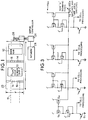
- Figure 1 is a front view of a standard two-channel recording head with the integrated chip mounted between the write/read gaps.
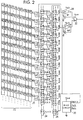
- Figure 2 is a diagram of the tape hole detection arrangement.
- Figure 3 is a diagram of the pixel current copying and summing circuitry.
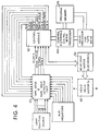
- Figure 4 is a diagram of the control environment for the combined tape edge and the tape hole detector chip.
- Figure 1 shows an integrated CMOS chip 10 mounted on a typical magnetic recording head 20.
- the active surface of the chip 10 is facing a magnetic tape 18 and is mounted on a magnetic recording head 20 using tape automated bonding technology.
- the active surface of the chip 10 is protected by metal layers, and an array of windows is created during metallization. Details of this system are included in co-pending U.S. Patent application, Serial No. , the disclosure of which is fully incorporated herein by reference.
- a light source illuminates the tape 18 and the surface of the chip 10 which is not covered by the tape 18.
- the tape 18 runs in close proximity to the surface of the chip 10 thereby creating a sharply defined boundary between the shadow area and the illuminated area on the active surface of the chip 10.
- the same photodetectors as used for the edge detector in co-pending U.S. Patent application Serial No. are also used for the hole detector.
- the tape hole detector 40 in Figure 4 has a programmable detection threshold level.
- the threshold level is set indirectly by an external controller module 42 as shown in Figure 4.
- the hole detector 40 is, therefore, freely programmable both with respect to threshold level detection and for high spatial resolution used for the location of the holes.
- the position(s) where the defined tape holes or tape hole patterns will appear when the tape is moving is computed.
- Blocks of pixel rows are selected -- for example, one block where the holes are anticipated and one where the holes are not expected to appear.
- Output currents from the individual pixels are summed, and the output from one block is then subtracted from the output of the other block.
- the extent to which such integration is used depends on the parameters of the actual system, and the extent to which ground level noise is present.
- Figure 4 shows the additional signal and clock lines required.
- the tape edge detector array 22 of processing cells is shown in Figure 2. Shaded areas of the cells indicate photosensitive regions of each cell. One extra line per cell is required from each pixel cell to allow for a simple physical mask layout by summing currents from individual pixels on a row-by-row basis. Figure 2 shows 12 row currents on lines R1 to R12.
- FIG. 3 shows the implementation of the array and summation from Figure 2.
- the row N summing node receives input currents from all pixels.
- Phototransistor Q1 of the leftmost cell delivers a current which passes through diode-connected transistors Q2 and Q3 which sets up a logarithmically compressed signal voltage which goes to the local processing cell of the edge detector. A copy of the photo current is then made by Q4. Therefore, the only difficulty faced by integrating the tape hole detection within the tape edge cells is the very small area required for each of the Q4 transistors.
- the Q1 and Q2/Q3 transistors implement the functions of the "PIXEL" and "LOG" blocks shown in the co-pending U.S. Patent application, Serial No. .
- the Q1 phototransistor may equally well be another type of sensor, such as, a PIN-diode. Which type to use will depend on the specific application, illumination levels and response speed requirements.
- Selection of rows for signal and reference currents is performed by clocking in patterns of "zeros" and “ones” on the input lines “RANGE HOLE” and “RANGE TAPE” to two columns of shift registers 24, 26 using clocks “CLK3" and “CLK4", respectively, as indicated in Figure 2.
- the content of the shift registers 24, 26 determines the state of the tape hole switches 25 and the tape area switches 27.
- the currents on rows R1 to R4, in which the light through the tape holes is expected to appear are switched to and summed on the signal current line which goes to the uppermost current sensing amplifier 28.
- the signal node is kept at a constant potential set up on the VREF3 output line from the bias circuit 30 due to feedback from the p-channel transistor Q1.
- a "dark" current mainly resulting from the translucency of the tape medium itself exists. This current comes from four rows where all pixels are covered by the tape medium. This is considered a no-signal current of "4 dark current units.”
- the phototransistors and current mirrors which deliver the individual currents operate in the sub-threshold region, i.e. in the pA or lower nA range when no signal is present. Summing a large number of these currents gives a current in the sub-threshold range, and the gate of transistor Q1 is kept at about 500 mV below the VREF3 voltage.
- the currents on rows R5 to R7 are output to the VREF3 node.
- the switching routes are set up by "not” enabling the corresponding tape hole switches 25 and the tape area switches 27.
- the purpose of this is to discard those currents which are within a tolerance band for the tape hole positions in the area between the tape edge and the holes or in the areas in the chip outside the tape where the photodetectors always respond to the light.
- the last-mentioned rows are not shown in Figure 2. Typically, much more than the three rows which are shown are necessary to account for all variations in tape hole positions.
- the sum of the currents from the five rows R8 to R12 are used as a reference current fed to the lower current sense amplifier 29.
- the states of the corresponding switches 25, 27 are shown in Figure 2.
- the selected number of reference rows must always be greater than the number of signal rows so that the voltage output from the lower current sense amplifier 29 (the voltage on the gate of Q2) is always less than the voltage at the output of the upper current sense amplifier 28 when tape holes are not present. This allows for an inherent “soft" and programmable threshold level for hole detection.
- the light which comes through the tape holes causes a signal current input to the upper current sense amplifier 28.
- this current is greater than the reference current, the voltage on the negative input of a comparator 32 will be lower than the voltage on the positive input, and the output of the comparator 32 goes “high", indicating the presence of a hole.
- This signal is monitored by the signalling from the controller module 42 to a control, filtering and digital servo processor 44 shown in Figure 4. During the loading of the shift registers 24, 26, the voltage on the "HOLE" line may toggle, but this is ignored by the control functions.
- Detection is, therefore, based upon differential sensing of voltages in an inherently noise-immune method. Further, a large dynamic range due to the logarithmic compression performed by the p-channel feedback transistors of the current sense amplifiers 28, 29 ensures that voltage compliance at the input of the comparator 32 is satisfied. The row selection and current switching process takes place without any generation of voltage spikes or charging of stray capacitances. This ensures that a large array of switches may be quickly controlled and set up.
- the tape hole detector 40 may also be used to check the computed position of the edge during the initial static edge location process in addition to comparing the computed tape width with the known tape width range stored in memory 46. This results in an edge resolution that will be coarse, but more than sufficient to allow for tape run-out detection.
- a tape edge detector 40 finds an edge, the tape hole detector 40 looks for the edge by enabling a few rows outside the edge and a few but larger number of rows inside the tape edge. A very small guard-band or no guard-band at all between blocks of rows can be used during this process. Then, the two blocks of rows are shifted up or down so that all active rows are either below or above the tape edge. With a correctly programmed threshold level, no output on the "HOLE" signal line will exist for these two positions of the active blocks.
- a full tape edge search is performed by the controller module 42.
- a self test of the tape hole detector 40 is performed by varying the number of signal rows and reference rows to see that the state of the "HOLE" signal line changes when selecting more signal rows than reference rows and vice-versa.
- the recording head is moved by the head drive motor 48 prior to this process to a mechanical end-stop position so that the active rows can be placed outside the location of the tape.
- Head drive motor electronics 50 receive signals from the controller module 42 to activate positioning of the head with the head drive motor 48.
- the self test is completed, the correct threshold level for edge detection is set up again. Then, the two or three active blocks of rows are moved over the whole operating range of the detector 40. If no tape edge exists, "tape run-out" is reported, and the tape cartridge is ejected for inspection by a user. An error message may then be given to the user.
- holes in the tape include a single hole or a pattern of holes. Also, “holes” include physically punched holes in the tape and holes in the magnetic layer itself, i.e. if there is no hole or holes in the tape substrate.
Landscapes
- Photometry And Measurement Of Optical Pulse Characteristics (AREA)
Applications Claiming Priority (2)
| Application Number | Priority Date | Filing Date | Title |
|---|---|---|---|
| US814840 | 1991-12-31 | ||
| US07/814,840 US5229620A (en) | 1991-12-31 | 1991-12-31 | System for integrated tape hole detection by detecting an edge of the tape and/or a pattern on the tape |
Publications (2)
| Publication Number | Publication Date |
|---|---|
| EP0549845A1 true EP0549845A1 (de) | 1993-07-07 |
| EP0549845B1 EP0549845B1 (de) | 1998-07-08 |
Family
ID=25216131
Family Applications (1)
| Application Number | Title | Priority Date | Filing Date |
|---|---|---|---|
| EP92105131A Expired - Lifetime EP0549845B1 (de) | 1991-12-31 | 1992-03-25 | System für integrierter Lochfeststellung im Band |
Country Status (3)
| Country | Link |
|---|---|
| US (1) | US5229620A (de) |
| EP (1) | EP0549845B1 (de) |
| DE (1) | DE69226159T2 (de) |
Cited By (2)
| Publication number | Priority date | Publication date | Assignee | Title |
|---|---|---|---|---|
| WO1999028909A1 (en) * | 1997-12-01 | 1999-06-10 | Storage Technology Corporation | Optical servo system for a tape drive |
| US7255908B2 (en) | 1997-10-22 | 2007-08-14 | Quantum Corporation | Magnetic tape |
Families Citing this family (15)
| Publication number | Priority date | Publication date | Assignee | Title |
|---|---|---|---|---|
| EP0569610B1 (de) * | 1992-05-13 | 1997-03-05 | Tandberg Data A/S | Methode und Vorrichtung zur Bestimmung der Bandposition für ein Band unter Verwendung eines speziellen Servo-Formates |
| DE19506467A1 (de) * | 1995-02-24 | 1996-08-29 | Koenig & Bauer Albert Ag | Vorrichtung und Verfahren zum Messen einer Lage einer Kante von Bahnen oder Bogen |
| US7029726B1 (en) | 1999-07-27 | 2006-04-18 | Quantum Corporation | Method for forming a servo pattern on a magnetic tape |
| GB2335785B (en) | 1998-03-24 | 2002-09-18 | Quantum Corp | Multi-channel magnetic tape system having optical tracking servo |
| US7153366B1 (en) | 1998-03-24 | 2006-12-26 | Quantum Corporation | Systems and method for forming a servo pattern on a magnetic tape |
| AU2441099A (en) | 1999-02-16 | 2000-09-04 | Quantum Corporation | Method of writing servo signal on magnetic tape |
| WO2000049605A1 (en) | 1999-02-17 | 2000-08-24 | Quantum Corporation | Method of writing servo signal on magnetic tape |
| US6961200B2 (en) * | 1999-07-27 | 2005-11-01 | Quantum Corporation | Optical servo track identification on tape storage media |
| US6558774B1 (en) | 1999-08-17 | 2003-05-06 | Quantum Corporation | Multiple-layer backcoating for magnetic tape |
| US6940676B1 (en) | 2000-06-07 | 2005-09-06 | Quantum Corporation | Triple push-pull optical tracking system |
| US6940681B2 (en) | 2001-08-20 | 2005-09-06 | Quantum Corporation | Optical to magnetic alignment in magnetic tape system |
| US7023650B2 (en) | 2001-11-07 | 2006-04-04 | Quantum Corporation | Optical sensor to recording head alignment |
| US7187515B2 (en) * | 2003-02-05 | 2007-03-06 | Quantum Corporation | Method and system for tracking magnetic media with embedded optical servo tracks |
| US6980390B2 (en) * | 2003-02-05 | 2005-12-27 | Quantum Corporation | Magnetic media with embedded optical servo tracks |
| DE102006043956A1 (de) * | 2006-09-14 | 2008-04-03 | Deutsche Thomson Ohg | Filmabtaster und Erfassungsvorrichtung dafür |
Citations (7)
| Publication number | Priority date | Publication date | Assignee | Title |
|---|---|---|---|---|
| US3637991A (en) * | 1969-04-14 | 1972-01-25 | Tokyo Shibaura Electric Co | Photoelectric readout apparatus |
| US3838291A (en) * | 1973-05-17 | 1974-09-24 | Hewlett Packard Co | Detector indicating availability and position of tape |
| EP0119568A2 (de) * | 1983-03-19 | 1984-09-26 | GRUNDIG E.M.V. Elektro-Mechanische Versuchsanstalt Max Grundig holländ. Stiftung & Co. KG. | Optoelektronische Bandendabschaltung |
| US4802030A (en) * | 1986-06-25 | 1989-01-31 | Hewlett-Packard Company | Head-tape alignment apparatus with a tape edge find operation |
| EP0347074A2 (de) * | 1988-06-17 | 1989-12-20 | Minnesota Mining And Manufacturing Company | Magnetbandkassetten - Identifizierung |
| EP0390555A2 (de) * | 1989-03-31 | 1990-10-03 | Sharp Kabushiki Kaisha | Magnetisches Aufzeichnungs-/Wiedergabegerät |
| US5050017A (en) * | 1989-08-23 | 1991-09-17 | Eastman Kodak Company | Memory guided magnetic tape tracking |
Family Cites Families (13)
| Publication number | Priority date | Publication date | Assignee | Title |
|---|---|---|---|---|
| NL7712418A (nl) * | 1977-11-11 | 1979-05-15 | Philips Nv | Opteken- en/of weergeefinrichting voor een bandvormige magnetische registratiedrager voor- zien van een regelsysteem voor de positionering van de magneetkop. |
| JPS55132522A (en) * | 1979-04-02 | 1980-10-15 | Olympus Optical Co Ltd | Automatic tracking method for magnetic tape |
| JPS56101622A (en) * | 1980-01-18 | 1981-08-14 | Olympus Optical Co Ltd | Autotracking system |
| US4329060A (en) * | 1980-04-14 | 1982-05-11 | Sangamo Weston, Inc. | Non-contacting workpiece gauging system |
| DE3112886A1 (de) * | 1981-03-31 | 1982-10-14 | Tandberg Data A/S, Oslo | Verfahren zum erkennen einer kante eines magnetischen mediums und vorrichtung zur druchfuehrung des verfahrens |
| DE3380538D1 (en) * | 1982-11-29 | 1989-10-12 | Tandberg Data | Arrangement for positioning a magnetic head on several tape tracks |
| DE3347632A1 (de) * | 1983-12-30 | 1985-07-11 | Tandberg Data A/S, Oslo | Anordnung zum positionieren eines wandlers auf mindestens einer spur eines bandfoermigen aufzeichnungstraegers |
| US4662757A (en) * | 1984-05-18 | 1987-05-05 | Rca Corporation | Motion tracking system and method |
| EP0190555B1 (de) * | 1985-02-08 | 1989-01-18 | Tandberg Data A/S | Verfahren und Anordnung zum Positionieren eines Magnetkopfs auf verschiedene Spuren eines Magnetbands |
| JPS63276738A (ja) * | 1987-01-27 | 1988-11-15 | Yamaha Corp | 磁気記録再生装置 |
| US4827141A (en) * | 1987-10-26 | 1989-05-02 | Hughes Aircraft Company | Subresolution element spatial measurement technique |
| US4886976A (en) * | 1988-12-28 | 1989-12-12 | Pitney Bowes Inc. | Driver circuitry for multiple sensors |
| US5107127A (en) * | 1990-08-13 | 1992-04-21 | Eastman Kodak Company | Method and apparatus for precision location of a perforation |
-
1991
- 1991-12-31 US US07/814,840 patent/US5229620A/en not_active Expired - Fee Related
-
1992
- 1992-03-25 DE DE69226159T patent/DE69226159T2/de not_active Expired - Fee Related
- 1992-03-25 EP EP92105131A patent/EP0549845B1/de not_active Expired - Lifetime
Patent Citations (7)
| Publication number | Priority date | Publication date | Assignee | Title |
|---|---|---|---|---|
| US3637991A (en) * | 1969-04-14 | 1972-01-25 | Tokyo Shibaura Electric Co | Photoelectric readout apparatus |
| US3838291A (en) * | 1973-05-17 | 1974-09-24 | Hewlett Packard Co | Detector indicating availability and position of tape |
| EP0119568A2 (de) * | 1983-03-19 | 1984-09-26 | GRUNDIG E.M.V. Elektro-Mechanische Versuchsanstalt Max Grundig holländ. Stiftung & Co. KG. | Optoelektronische Bandendabschaltung |
| US4802030A (en) * | 1986-06-25 | 1989-01-31 | Hewlett-Packard Company | Head-tape alignment apparatus with a tape edge find operation |
| EP0347074A2 (de) * | 1988-06-17 | 1989-12-20 | Minnesota Mining And Manufacturing Company | Magnetbandkassetten - Identifizierung |
| EP0390555A2 (de) * | 1989-03-31 | 1990-10-03 | Sharp Kabushiki Kaisha | Magnetisches Aufzeichnungs-/Wiedergabegerät |
| US5050017A (en) * | 1989-08-23 | 1991-09-17 | Eastman Kodak Company | Memory guided magnetic tape tracking |
Non-Patent Citations (2)
| Title |
|---|
| IBM TECHNICAL DISCLOSURE BULLETIN. vol. 18, no. 1, June 1975, NEW YORK US pages 213 - 215 KELLER ET AL. 'SENSING DEVICE FOR HOLES IN TRAVELLING TAPE' * |
| PATENT ABSTRACTS OF JAPAN vol. 7, no. 180 (P-215)(1325) 9 August 1983 & JP-A-58 083 351 ( NIHON SHIYUUHENKI K.K. ) 19 May 1983 * |
Cited By (6)
| Publication number | Priority date | Publication date | Assignee | Title |
|---|---|---|---|---|
| US7255908B2 (en) | 1997-10-22 | 2007-08-14 | Quantum Corporation | Magnetic tape |
| WO1999028909A1 (en) * | 1997-12-01 | 1999-06-10 | Storage Technology Corporation | Optical servo system for a tape drive |
| US6084740A (en) * | 1997-12-01 | 2000-07-04 | Storage Technology Corporation | Optical servo system for a tape drive |
| US6236529B1 (en) | 1997-12-01 | 2001-05-22 | Storage Technology Corporation | Optical servo system for a tape drive |
| US6480351B2 (en) | 1997-12-01 | 2002-11-12 | Storage Technology Corporation | Optical servo system for a tape drive |
| US6549363B2 (en) | 1997-12-01 | 2003-04-15 | Storage Technology Corporation | Optical servo system for a tape drive |
Also Published As
| Publication number | Publication date |
|---|---|
| DE69226159D1 (de) | 1998-08-13 |
| EP0549845B1 (de) | 1998-07-08 |
| DE69226159T2 (de) | 1998-11-19 |
| US5229620A (en) | 1993-07-20 |
Similar Documents
| Publication | Publication Date | Title |
|---|---|---|
| US5229620A (en) | System for integrated tape hole detection by detecting an edge of the tape and/or a pattern on the tape | |
| EP0549848B1 (de) | Verfahren und Vorrichtung zum Detektieren einer Magnetbandkante und Verwendung der Vorrichtung | |
| JP3581031B2 (ja) | 光検出装置 | |
| JP4027308B2 (ja) | 受光装置信号に対するオフセット除去及び空間周波数帯域フィルタリング回路及び方法 | |
| WO1993018555A1 (en) | Integrated solid state light emitting and detecting array and apparatus employing said array | |
| KR102886690B1 (ko) | 인접-게이트 스위칭 픽셀 센서 | |
| EP1249789A1 (de) | Photodetektorvorrichtung | |
| JPH09233259A (ja) | 光受容回路 | |
| EP0555511B1 (de) | Vorrichtung und Verfahren für die Führung einer Bandkante kompatibel mit einem dafür bestimmten Bandservoformat | |
| US5155353A (en) | High dynamic range integrated opto-electronic sensor and MOSFET amplifiers for pulsed light | |
| US4127781A (en) | Scan mirror position determining system | |
| CA1224255A (en) | Optical end-of-tape detection device | |
| KR20050026704A (ko) | 광 감지 장치 | |
| US6917030B2 (en) | Photo-sensor array with pixel-level signal comparison | |
| EP0604517B1 (de) | Rückgewinnung der tonsignalen von einer optischen aufzeichnung von variabeler breite | |
| US3772662A (en) | Write ring detector for magnetic recorders | |
| CA1289217C (en) | Photodetector having cascaded photoelements | |
| EP1313061B1 (de) | System und Verfahren zur Tastung von einem Photodetektor sowie hiermit ausgerüstete Photozellenschaltungen | |
| US5144286A (en) | Photosensitive switch with circuit for indicating malfunction | |
| US4633346A (en) | Magnetic head positioning device for a flexible disk | |
| JPH0581630A (ja) | 記録再生素子の位置検出装置 | |
| US12196584B2 (en) | Multi-track optical encoder | |
| JP3002120B2 (ja) | 画像処理装置 | |
| SU468270A1 (ru) | След ща система дл устройства считывани графической информации | |
| JPH04334288A (ja) | 監視用vtrシステム |
Legal Events
| Date | Code | Title | Description |
|---|---|---|---|
| PUAI | Public reference made under article 153(3) epc to a published international application that has entered the european phase |
Free format text: ORIGINAL CODE: 0009012 |
|
| AK | Designated contracting states |
Kind code of ref document: A1 Designated state(s): DE FR GB |
|
| 17P | Request for examination filed |
Effective date: 19931210 |
|
| 17Q | First examination report despatched |
Effective date: 19960110 |
|
| GRAG | Despatch of communication of intention to grant |
Free format text: ORIGINAL CODE: EPIDOS AGRA |
|
| GRAG | Despatch of communication of intention to grant |
Free format text: ORIGINAL CODE: EPIDOS AGRA |
|
| GRAH | Despatch of communication of intention to grant a patent |
Free format text: ORIGINAL CODE: EPIDOS IGRA |
|
| GRAH | Despatch of communication of intention to grant a patent |
Free format text: ORIGINAL CODE: EPIDOS IGRA |
|
| RAP1 | Party data changed (applicant data changed or rights of an application transferred) |
Owner name: TANDBERG DATA ASA |
|
| GRAA | (expected) grant |
Free format text: ORIGINAL CODE: 0009210 |
|
| AK | Designated contracting states |
Kind code of ref document: B1 Designated state(s): DE FR GB |
|
| REF | Corresponds to: |
Ref document number: 69226159 Country of ref document: DE Date of ref document: 19980813 |
|
| ET | Fr: translation filed | ||
| PLBE | No opposition filed within time limit |
Free format text: ORIGINAL CODE: 0009261 |
|
| STAA | Information on the status of an ep patent application or granted ep patent |
Free format text: STATUS: NO OPPOSITION FILED WITHIN TIME LIMIT |
|
| 26N | No opposition filed | ||
| PGFP | Annual fee paid to national office [announced via postgrant information from national office to epo] |
Ref country code: FR Payment date: 20000310 Year of fee payment: 9 |
|
| PGFP | Annual fee paid to national office [announced via postgrant information from national office to epo] |
Ref country code: GB Payment date: 20000322 Year of fee payment: 9 |
|
| PG25 | Lapsed in a contracting state [announced via postgrant information from national office to epo] |
Ref country code: GB Free format text: LAPSE BECAUSE OF NON-PAYMENT OF DUE FEES Effective date: 20010325 |
|
| PGFP | Annual fee paid to national office [announced via postgrant information from national office to epo] |
Ref country code: DE Payment date: 20010326 Year of fee payment: 10 |
|
| GBPC | Gb: european patent ceased through non-payment of renewal fee |
Effective date: 20010325 |
|
| PG25 | Lapsed in a contracting state [announced via postgrant information from national office to epo] |
Ref country code: FR Free format text: LAPSE BECAUSE OF NON-PAYMENT OF DUE FEES Effective date: 20011130 |
|
| REG | Reference to a national code |
Ref country code: FR Ref legal event code: ST |
|
| PG25 | Lapsed in a contracting state [announced via postgrant information from national office to epo] |
Ref country code: DE Free format text: LAPSE BECAUSE OF NON-PAYMENT OF DUE FEES Effective date: 20021001 |