EP0550021A2 - Formation auto-alignée à masque unique de CMOS-BICMOS à double-puits avec topographie à surface platte - Google Patents
Formation auto-alignée à masque unique de CMOS-BICMOS à double-puits avec topographie à surface platte Download PDFInfo
- Publication number
- EP0550021A2 EP0550021A2 EP92121935A EP92121935A EP0550021A2 EP 0550021 A2 EP0550021 A2 EP 0550021A2 EP 92121935 A EP92121935 A EP 92121935A EP 92121935 A EP92121935 A EP 92121935A EP 0550021 A2 EP0550021 A2 EP 0550021A2
- Authority
- EP
- European Patent Office
- Prior art keywords
- dielectric
- recited
- substrate
- conductivity type
- mask
- Prior art date
- Legal status (The legal status is an assumption and is not a legal conclusion. Google has not performed a legal analysis and makes no representation as to the accuracy of the status listed.)
- Withdrawn
Links
Images
Classifications
-
- H—ELECTRICITY
- H10—SEMICONDUCTOR DEVICES; ELECTRIC SOLID-STATE DEVICES NOT OTHERWISE PROVIDED FOR
- H10D—INORGANIC ELECTRIC SEMICONDUCTOR DEVICES
- H10D84/00—Integrated devices formed in or on semiconductor substrates that comprise only semiconducting layers, e.g. on Si wafers or on GaAs-on-Si wafers
- H10D84/01—Manufacture or treatment
- H10D84/0123—Integrating together multiple components covered by H10D12/00 or H10D30/00, e.g. integrating multiple IGBTs
- H10D84/0126—Integrating together multiple components covered by H10D12/00 or H10D30/00, e.g. integrating multiple IGBTs the components including insulated gates, e.g. IGFETs
- H10D84/0165—Integrating together multiple components covered by H10D12/00 or H10D30/00, e.g. integrating multiple IGBTs the components including insulated gates, e.g. IGFETs the components including complementary IGFETs, e.g. CMOS devices
- H10D84/0191—Manufacturing their doped wells
-
- H—ELECTRICITY
- H10—SEMICONDUCTOR DEVICES; ELECTRIC SOLID-STATE DEVICES NOT OTHERWISE PROVIDED FOR
- H10D—INORGANIC ELECTRIC SEMICONDUCTOR DEVICES
- H10D84/00—Integrated devices formed in or on semiconductor substrates that comprise only semiconducting layers, e.g. on Si wafers or on GaAs-on-Si wafers
- H10D84/01—Manufacture or treatment
- H10D84/02—Manufacture or treatment characterised by using material-based technologies
- H10D84/03—Manufacture or treatment characterised by using material-based technologies using Group IV technology, e.g. silicon technology or silicon-carbide [SiC] technology
- H10D84/038—Manufacture or treatment characterised by using material-based technologies using Group IV technology, e.g. silicon technology or silicon-carbide [SiC] technology using silicon technology, e.g. SiGe
-
- H—ELECTRICITY
- H10—SEMICONDUCTOR DEVICES; ELECTRIC SOLID-STATE DEVICES NOT OTHERWISE PROVIDED FOR
- H10P—GENERIC PROCESSES OR APPARATUS FOR THE MANUFACTURE OR TREATMENT OF DEVICES COVERED BY CLASS H10
- H10P30/00—Ion implantation into wafers, substrates or parts of devices
- H10P30/20—Ion implantation into wafers, substrates or parts of devices into semiconductor materials, e.g. for doping
- H10P30/22—Ion implantation into wafers, substrates or parts of devices into semiconductor materials, e.g. for doping using masks
-
- H—ELECTRICITY
- H10—SEMICONDUCTOR DEVICES; ELECTRIC SOLID-STATE DEVICES NOT OTHERWISE PROVIDED FOR
- H10D—INORGANIC ELECTRIC SEMICONDUCTOR DEVICES
- H10D84/00—Integrated devices formed in or on semiconductor substrates that comprise only semiconducting layers, e.g. on Si wafers or on GaAs-on-Si wafers
- H10D84/40—Integrated devices formed in or on semiconductor substrates that comprise only semiconducting layers, e.g. on Si wafers or on GaAs-on-Si wafers characterised by the integration of at least one component covered by groups H10D12/00 or H10D30/00 with at least one component covered by groups H10D10/00 or H10D18/00, e.g. integration of IGFETs with BJTs
- H10D84/401—Combinations of FETs or IGBTs with BJTs
-
- H—ELECTRICITY
- H10—SEMICONDUCTOR DEVICES; ELECTRIC SOLID-STATE DEVICES NOT OTHERWISE PROVIDED FOR
- H10D—INORGANIC ELECTRIC SEMICONDUCTOR DEVICES
- H10D84/00—Integrated devices formed in or on semiconductor substrates that comprise only semiconducting layers, e.g. on Si wafers or on GaAs-on-Si wafers
- H10D84/80—Integrated devices formed in or on semiconductor substrates that comprise only semiconducting layers, e.g. on Si wafers or on GaAs-on-Si wafers characterised by the integration of at least one component covered by groups H10D12/00 or H10D30/00, e.g. integration of IGFETs
- H10D84/82—Integrated devices formed in or on semiconductor substrates that comprise only semiconducting layers, e.g. on Si wafers or on GaAs-on-Si wafers characterised by the integration of at least one component covered by groups H10D12/00 or H10D30/00, e.g. integration of IGFETs of only field-effect components
- H10D84/83—Integrated devices formed in or on semiconductor substrates that comprise only semiconducting layers, e.g. on Si wafers or on GaAs-on-Si wafers characterised by the integration of at least one component covered by groups H10D12/00 or H10D30/00, e.g. integration of IGFETs of only field-effect components of only insulated-gate FETs [IGFET]
- H10D84/85—Complementary IGFETs, e.g. CMOS
- H10D84/859—Complementary IGFETs, e.g. CMOS comprising both N-type and P-type wells, e.g. twin-tub
Definitions
- CMOS and BiCMOS technologies employ twin (n and p) wells in order to allow simultaneous optimization of the NMOS and PMOS transistors.
- the conventional twin well formation processes employ one or two microlithography masking steps.
- the two-mask fabrication process has the advantage that it does not degrade the silicon surface planarity or topography. This is an important requirement in advanced sub-0.5 ⁇ m CMOS and BiCMOS technologies where even a small (e.g. a few thousand ⁇ ) step between the n-well and p-well regions can result in gate length variations between the NMOS and PMOS transistors (due to the limited depth-of-focus orDOF budget in advanced photo-lithography tools).
- CMOS transistor gate length variations can degrade manufacturability and yield.
- the process simplicity of the conventional one-mask fabrication process is not a strong and sufficient advantage/improvement to justify its use in sub-0.5 ⁇ m semiconductor technologies since the one-mask process consumes silicon when masking a particular area to provide a well region.
- Such oxidation-induced silicon consumption results in uneven planarity of the PMOS and NMOS gates as shall be explained below.
- the potential gate length variability caused by the nonplanar n and p well surfaces ad DOF limitation imposes the above-mentioned obstacle.
- the surface topography problem in the conventional one-mask fabrication process is generated by a selective thermal oxidation process.
- An oxide/nitride stack is patterned and is used (usually along with the photoresist mask) as an ion implantation mask to define one of the wells.
- an oxidation step is performed which selectively defines an oxide hard mask over the implanted region.
- a second ion implantation step is used to define the second (opposite) well regions.
- a surface topography or step is produced between the n and p well regions due to the silicon consumption by the selective thermal oxidation step.
- CMOS and BiCMOS technologies usually rely on a two-mask (non-self aligned) process to define the n-well and p-well regions.
- patterned photoresist (or hard mask) layers are used as ion implantation masks. No surface step or topography is produced, therefore allowing uniform PMOS and NMOS gate patterning.
- the use of one additional masking process adds to the overall process cost and complexity.
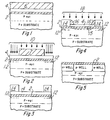
- Figures 1 through 5 illustrate cross-sectional drawings of the resulting structure from the following processing steps.
- a single-mask self-aligned process is disclosed for formation of n and p wells for advanced CMOS and BiCMOS technologies.
- the proposed process forms n-well and p-well regions using a single microlithography masking step along with a selective semiconductor (Si or GeSi) growth (SSG) process without producing surface topography or degrading surface planarity.
- Si or GeSi selective semiconductor growth
- This simple process ensures uniform NMOS and PMOS gate patterning due to fat surface topography.
- the n-to-p well placement is self-aligned due to the use of a disposable SSG hard mask.
- the invention provides a single-mask self-aligned twin well formation process for advanced CMOS and BiCMOS technologies.
- the process is based on the use of a selectively grown semiconductor (or metal) hard mask.
- the process flow for the preferred embodiment of the process flow is as follows:
Landscapes
- Metal-Oxide And Bipolar Metal-Oxide Semiconductor Integrated Circuits (AREA)
Applications Claiming Priority (2)
| Application Number | Priority Date | Filing Date | Title |
|---|---|---|---|
| US814547 | 1991-12-30 | ||
| US07/814,547 US5252501A (en) | 1991-12-30 | 1991-12-30 | Self-aligned single-mask CMOS/BiCMOS twin-well formation with flat surface topography |
Publications (2)
| Publication Number | Publication Date |
|---|---|
| EP0550021A2 true EP0550021A2 (fr) | 1993-07-07 |
| EP0550021A3 EP0550021A3 (en) | 1996-12-27 |
Family
ID=25215385
Family Applications (1)
| Application Number | Title | Priority Date | Filing Date |
|---|---|---|---|
| EP92121935A Withdrawn EP0550021A3 (en) | 1991-12-30 | 1992-12-23 | Self-aligned single-mask cmos/bicmos twin-well formation with flat surface topography |
Country Status (4)
| Country | Link |
|---|---|
| US (1) | US5252501A (fr) |
| EP (1) | EP0550021A3 (fr) |
| JP (1) | JPH06112420A (fr) |
| TW (1) | TW217461B (fr) |
Cited By (3)
| Publication number | Priority date | Publication date | Assignee | Title |
|---|---|---|---|---|
| EP0696062A3 (fr) * | 1994-07-28 | 1996-12-11 | Hitachi Ltd | Dispositif semi-conducteur CMOS et procédé de fabrication associé |
| DE19603794A1 (de) * | 1995-07-26 | 1997-01-30 | Lg Semicon Co Ltd | Verfahren zum Ausbilden einer Doppelsenke für Halbleiteranordnungen |
| WO2007010732A1 (fr) * | 2005-07-19 | 2007-01-25 | Nissan Motor Co., Ltd. | Procédé de fabrication de dispositif à semi-conducteurs |
Families Citing this family (13)
| Publication number | Priority date | Publication date | Assignee | Title |
|---|---|---|---|---|
| US5770492A (en) * | 1995-06-07 | 1998-06-23 | Lsi Logic Corporation | Self-aligned twin well process |
| US5583062A (en) * | 1995-06-07 | 1996-12-10 | Lsi Logic Corporation | Self-aligned twin well process having a SiO2 -polysilicon-SiO2 barrier mask |
| US5763302A (en) * | 1995-06-07 | 1998-06-09 | Lsi Logic Corporation | Self-aligned twin well process |
| US5670393A (en) * | 1995-07-12 | 1997-09-23 | Lsi Logic Corporation | Method of making combined metal oxide semiconductor and junction field effect transistor device |
| US5547894A (en) * | 1995-12-21 | 1996-08-20 | International Business Machines Corporation | CMOS processing with low and high-current FETs |
| US5670395A (en) * | 1996-04-29 | 1997-09-23 | Chartered Semiconductor Manufacturing Pte. Ltd. | Process for self-aligned twin wells without N-well and P-well height difference |
| DE59813593D1 (de) * | 1997-04-29 | 2006-07-27 | Infineon Technologies Ag | Verfahren zur Herstellung einer CMOS-Schaltungsanordnung |
| US5956583A (en) * | 1997-06-30 | 1999-09-21 | Fuller; Robert T. | Method for forming complementary wells and self-aligned trench with a single mask |
| US6307230B1 (en) * | 1999-01-05 | 2001-10-23 | Texas Instruments Incorporated | Transistor having an improved sidewall gate structure and method of construction |
| US6235568B1 (en) * | 1999-01-22 | 2001-05-22 | Intel Corporation | Semiconductor device having deposited silicon regions and a method of fabrication |
| US6207538B1 (en) | 1999-12-28 | 2001-03-27 | Taiwan Semiconductor Manufacturing Company | Method for forming n and p wells in a semiconductor substrate using a single masking step |
| DE10052680C2 (de) * | 2000-10-24 | 2002-10-24 | Advanced Micro Devices Inc | Verfahren zum Einstellen einer Form einer auf einem Substrat gebildeten Oxidschicht |
| US6586296B1 (en) * | 2001-04-30 | 2003-07-01 | Cypress Semiconductor Corp. | Method of doping wells, channels, and gates of dual gate CMOS technology with reduced number of masks |
Family Cites Families (7)
| Publication number | Priority date | Publication date | Assignee | Title |
|---|---|---|---|---|
| US4050965A (en) * | 1975-10-21 | 1977-09-27 | The United States Of America As Represented By The Secretary Of The Air Force | Simultaneous fabrication of CMOS transistors and bipolar devices |
| US4424621A (en) * | 1981-12-30 | 1984-01-10 | International Business Machines Corporation | Method to fabricate stud structure for self-aligned metallization |
| US4527325A (en) * | 1983-12-23 | 1985-07-09 | International Business Machines Corporation | Process for fabricating semiconductor devices utilizing a protective film during high temperature annealing |
| US4558508A (en) * | 1984-10-15 | 1985-12-17 | International Business Machines Corporation | Process of making dual well CMOS semiconductor structure with aligned field-dopings using single masking step |
| JPH01161752A (ja) * | 1987-12-18 | 1989-06-26 | Toshiba Corp | 半導体装置製造方法 |
| US5070029A (en) * | 1989-10-30 | 1991-12-03 | Motorola, Inc. | Semiconductor process using selective deposition |
| US5132241A (en) * | 1991-04-15 | 1992-07-21 | Industrial Technology Research Institute | Method of manufacturing minimum counterdoping in twin well process |
-
1991
- 1991-12-30 US US07/814,547 patent/US5252501A/en not_active Expired - Lifetime
-
1992
- 1992-12-23 EP EP92121935A patent/EP0550021A3/en not_active Withdrawn
-
1993
- 1993-01-04 JP JP5029576A patent/JPH06112420A/ja active Pending
- 1993-04-22 TW TW082103072A patent/TW217461B/zh active
Cited By (8)
| Publication number | Priority date | Publication date | Assignee | Title |
|---|---|---|---|---|
| EP0696062A3 (fr) * | 1994-07-28 | 1996-12-11 | Hitachi Ltd | Dispositif semi-conducteur CMOS et procédé de fabrication associé |
| US6368905B1 (en) | 1994-07-28 | 2002-04-09 | Hitachi, Ltd. | Process for manufacturing a semiconductor wafer, a semiconductor wafer, process for manufacturing a semiconductor integrated circuit device, and semiconductor integrated circuit device |
| US6630375B2 (en) | 1994-07-28 | 2003-10-07 | Hitachi, Ltd. | Process for manufacturing a semiconductor wafer, a semiconductor wafer, process for manufacturing a semiconductor integrated circuit device, and semiconductor integrated circuit device |
| US6806130B2 (en) | 1994-07-28 | 2004-10-19 | Renesas Technology Corp. | Process for manufacturing a semiconductor wafer, a semiconductor wafer, process for manufacturing a semiconductor integrated circuit device, and semiconductor integrated circuit device |
| DE19603794A1 (de) * | 1995-07-26 | 1997-01-30 | Lg Semicon Co Ltd | Verfahren zum Ausbilden einer Doppelsenke für Halbleiteranordnungen |
| DE19603794B4 (de) * | 1995-07-26 | 2004-06-03 | LG Semicon Co., Ltd., Cheongju | Verfahren zum Ausbilden einer Doppelwanne für Halbleiteranordnungen |
| WO2007010732A1 (fr) * | 2005-07-19 | 2007-01-25 | Nissan Motor Co., Ltd. | Procédé de fabrication de dispositif à semi-conducteurs |
| US7749845B2 (en) | 2005-07-19 | 2010-07-06 | Nissan Motor Co., Ltd. | Semiconductor device manufacturing method |
Also Published As
| Publication number | Publication date |
|---|---|
| EP0550021A3 (en) | 1996-12-27 |
| JPH06112420A (ja) | 1994-04-22 |
| TW217461B (fr) | 1993-12-11 |
| US5252501A (en) | 1993-10-12 |
Similar Documents
| Publication | Publication Date | Title |
|---|---|---|
| US5252501A (en) | Self-aligned single-mask CMOS/BiCMOS twin-well formation with flat surface topography | |
| US6930030B2 (en) | Method of forming an electronic device on a recess in the surface of a thin film of silicon etched to a precise thickness | |
| US6294416B1 (en) | Method of fabricating CMOS transistors with self-aligned planarization twin-well by using fewer mask counts | |
| US6245619B1 (en) | Disposable-spacer damascene-gate process for SUB 0.05 μm MOS devices | |
| US20040014292A1 (en) | Sub-micron MOS transistor | |
| US5654213A (en) | Method for fabricating a CMOS device | |
| US6033958A (en) | Method of fabricating dual voltage MOS transistors | |
| JP4751004B2 (ja) | 厚さが異なる領域を有するデバイスまたはデバイス層の製造方法 | |
| JPH10335480A (ja) | 半導体装置およびその製造方法 | |
| US6821836B2 (en) | Disposable spacer | |
| KR100507856B1 (ko) | Mos트랜지스터 제조방법 | |
| JPH02162761A (ja) | Mosfetの製造方法 | |
| US5976952A (en) | Implanted isolation structure formation for high density CMOS integrated circuits | |
| US5612242A (en) | Trench isolation method for CMOS transistor | |
| US5696016A (en) | Process for manufacturing a CMOSFET intergrated circuit | |
| EP0561167B1 (fr) | Méthode et structure d'un petit semi-conducteur | |
| US5714398A (en) | Self-aligned tungsten strapped source/drain and gate technology for deep submicron CMOS | |
| JPH05267331A (ja) | Mos型半導体装置の製造方法 | |
| US6657263B2 (en) | MOS transistors having dual gates and self-aligned interconnect contact windows | |
| US6251744B1 (en) | Implant method to improve characteristics of high voltage isolation and high voltage breakdown | |
| US6110788A (en) | Surface channel MOS transistors, methods for making the same, and semiconductor devices containing the same | |
| US6162714A (en) | Method of forming thin polygates for sub quarter micron CMOS process | |
| US6376293B1 (en) | Shallow drain extenders for CMOS transistors using replacement gate design | |
| EP0434182B1 (fr) | Procédé de fabrication de couches enterrées pour circuits intégrés | |
| US5946579A (en) | Stacked mask integration technique for advanced CMOS transistor formation |
Legal Events
| Date | Code | Title | Description |
|---|---|---|---|
| PUAI | Public reference made under article 153(3) epc to a published international application that has entered the european phase |
Free format text: ORIGINAL CODE: 0009012 |
|
| AK | Designated contracting states |
Kind code of ref document: A2 Designated state(s): DE FR GB IT NL |
|
| PUAL | Search report despatched |
Free format text: ORIGINAL CODE: 0009013 |
|
| AK | Designated contracting states |
Kind code of ref document: A3 Designated state(s): DE FR GB IT NL |
|
| 17P | Request for examination filed |
Effective date: 19970624 |
|
| 17Q | First examination report despatched |
Effective date: 20040824 |
|
| STAA | Information on the status of an ep patent application or granted ep patent |
Free format text: STATUS: THE APPLICATION IS DEEMED TO BE WITHDRAWN |
|
| 18D | Application deemed to be withdrawn |
Effective date: 20050105 |