EP0550974A2 - Méthode pour la fabrication de composants magnétiques multicouches - Google Patents
Méthode pour la fabrication de composants magnétiques multicouches Download PDFInfo
- Publication number
- EP0550974A2 EP0550974A2 EP92311246A EP92311246A EP0550974A2 EP 0550974 A2 EP0550974 A2 EP 0550974A2 EP 92311246 A EP92311246 A EP 92311246A EP 92311246 A EP92311246 A EP 92311246A EP 0550974 A2 EP0550974 A2 EP 0550974A2
- Authority
- EP
- European Patent Office
- Prior art keywords
- magnetic
- regions
- layer
- region
- layers
- Prior art date
- Legal status (The legal status is an assumption and is not a legal conclusion. Google has not performed a legal analysis and makes no representation as to the accuracy of the status listed.)
- Granted
Links
Images


Classifications
-
- H—ELECTRICITY
- H01—ELECTRIC ELEMENTS
- H01F—MAGNETS; INDUCTANCES; TRANSFORMERS; SELECTION OF MATERIALS FOR THEIR MAGNETIC PROPERTIES
- H01F41/00—Apparatus or processes specially adapted for manufacturing or assembling magnets, inductances or transformers; Apparatus or processes specially adapted for manufacturing materials characterised by their magnetic properties
- H01F41/14—Apparatus or processes specially adapted for manufacturing or assembling magnets, inductances or transformers; Apparatus or processes specially adapted for manufacturing materials characterised by their magnetic properties for applying magnetic films to substrates
- H01F41/16—Apparatus or processes specially adapted for manufacturing or assembling magnets, inductances or transformers; Apparatus or processes specially adapted for manufacturing materials characterised by their magnetic properties for applying magnetic films to substrates the magnetic material being applied in the form of particles, e.g. by serigraphy, to form thick magnetic films or precursors therefor
-
- B—PERFORMING OPERATIONS; TRANSPORTING
- B28—WORKING CEMENT, CLAY, OR STONE
- B28B—SHAPING CLAY OR OTHER CERAMIC COMPOSITIONS; SHAPING SLAG; SHAPING MIXTURES CONTAINING CEMENTITIOUS MATERIAL, e.g. PLASTER
- B28B1/00—Producing shaped prefabricated articles from the material
- B28B1/48—Producing shaped prefabricated articles from the material by removing material from solid section preforms for forming hollow articles, e.g. by punching or boring
-
- B—PERFORMING OPERATIONS; TRANSPORTING
- B28—WORKING CEMENT, CLAY, OR STONE
- B28B—SHAPING CLAY OR OTHER CERAMIC COMPOSITIONS; SHAPING SLAG; SHAPING MIXTURES CONTAINING CEMENTITIOUS MATERIAL, e.g. PLASTER
- B28B7/00—Moulds; Cores; Mandrels
- B28B7/34—Moulds, cores, or mandrels of special material, e.g. destructible materials
- B28B7/342—Moulds, cores, or mandrels of special material, e.g. destructible materials which are at least partially destroyed, e.g. broken, molten, before demoulding; Moulding surfaces or spaces shaped by, or in, the ground, or sand or soil, whether bound or not; Cores consisting at least mainly of sand or soil, whether bound or not
-
- Y—GENERAL TAGGING OF NEW TECHNOLOGICAL DEVELOPMENTS; GENERAL TAGGING OF CROSS-SECTIONAL TECHNOLOGIES SPANNING OVER SEVERAL SECTIONS OF THE IPC; TECHNICAL SUBJECTS COVERED BY FORMER USPC CROSS-REFERENCE ART COLLECTIONS [XRACs] AND DIGESTS
- Y10—TECHNICAL SUBJECTS COVERED BY FORMER USPC
- Y10T—TECHNICAL SUBJECTS COVERED BY FORMER US CLASSIFICATION
- Y10T29/00—Metal working
- Y10T29/49—Method of mechanical manufacture
- Y10T29/49002—Electrical device making
- Y10T29/4902—Electromagnet, transformer or inductor
-
- Y—GENERAL TAGGING OF NEW TECHNOLOGICAL DEVELOPMENTS; GENERAL TAGGING OF CROSS-SECTIONAL TECHNOLOGIES SPANNING OVER SEVERAL SECTIONS OF THE IPC; TECHNICAL SUBJECTS COVERED BY FORMER USPC CROSS-REFERENCE ART COLLECTIONS [XRACs] AND DIGESTS
- Y10—TECHNICAL SUBJECTS COVERED BY FORMER USPC
- Y10T—TECHNICAL SUBJECTS COVERED BY FORMER US CLASSIFICATION
- Y10T29/00—Metal working
- Y10T29/49—Method of mechanical manufacture
- Y10T29/49826—Assembling or joining
- Y10T29/49833—Punching, piercing or reaming part by surface of second part
Definitions
- This invention relates to methods for making multilayer magnetic components such as transformers and inductors, and, in particular, to an improved method for making such components employing removable spacer regions to form separated magnetic regions within an insulating body.
- Static magnetic devices such as transformers and inductors are essential elements in a wide variety of circuits requiring energy storage and conversion, impedance matching, filtering, EMI suppression, voltage and current transformation, and resonance. As historically constructed, these devices tended to be bulky, heavy and expensive to fabricate as compared with other circuit components. Manual operations such as winding conductive wire around magnetic cores dominated production costs.
- a new approach to the fabrication of such devices was described in United States Application S.N. 07/695653 entitled “Multilayer Monolithic Magnetic Components and Method of Making Same” filed by Grader et al and assigned to applicants' assignee.
- ceramic powders are mixed with organic binders to form magnetic and insulating (non-magnetic) green ceramic tapes, respectively.
- a magnetic device is made by forming layers having suitable two-dimensional patterns of magnetic and insulating regions and stacking the layers to form a structure with well-defined magnetic and insulating non-magnetic regions.
- Conductors are printed on the insulating regions as needed, and the resulting structure is laminated under low pressure in the range 500-3000 psi at a temperature of 60-80°C.
- the laminated structure is fired at a temperature between 800 to 1400°C to form a co-fired composite structure of the magnetic component.
- the magnetic and the insulating materials must have compatible sintering rates and temperatures. Such compatibility is achieved, for example, by doping the insulating material with metals.
- multilayer magnetic components can be made with reduced cracking and magnetic degradation by forming layers having patterns of magnetic and insulating regions separated by regions that are removable during sintering.
- layers of removable material are disposed between magnetic regions and insulating regions so as to produce upon sintering a magnetic core within an insulating body wherein the core is substantially completely surrounded by a thin layer of free space.
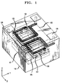
- FIG. 1 is a three-dimensional see-through drawing of an exemplary composite magnetic device.
- This device is constructed as a multiple winding transformer having a toroidal magnetic core.
- the toroidal core comprises four sections 101 to 104, each of which is constructed from a plurality of high magnetic permeability ceramic green tape layers. Sections 102 and 104 are circumscribed by conductive windings 105 and 106, respectively. These windings form the primary and secondary of a transformer. Alternatively, the windings could be connected in series so that the structure functions as a multiple turn inductor.
- Windings 105 and 106 are formed by printing pairs of conductor turns onto a plurality of insulating non-magnetic ceramic green tape layers, each insulating non-magnetic layer having suitable apertures for containing the sections of magnetic green tape layered inserts and peripheral regions of removable material disposed between the non-magnetic material and the magnetic material.
- the turns printed on each layer are connected to turns of the other layers with conductive vias 107 (i.e. through holes filled with conductive material).
- Additional insulating non-magnetic layers are used to contain sections 101 and 103 of the magnetic tape sections and to form the top and bottom structure of the component. In each instance regions of removable material (not shown in FIG. 1) have been provided to separate the magnetic and non-magnetic regions.
- Conductive vias 108 are used to connect the ends of windings 105 and 106 to connector pads 109 on the top surface of the device.
- the insulating non-magnetic regions of the structure are denoted by 110.
- Current excitation of the windings 105 and 106 produces a magnetic flux in the closed magnetic path defined by sections 101-104 of the toroidal core.
- the fluxpath in this embodiment is in a vertical XZ plane.
- the ceramic green tape layers used in the construction of the FIG. 1 device are advantageously those described in the aforementioned Grader et al application.
- the ceramic materials can be spinel ferrites of the form M 1+x Fe 2-y 0 4-z where the values for x, y and z can assume both positive and negative numerical values.
- the M material normally includes at least one of the elements Mn, Ni, Zn, Fe, Cu, Co, Zr, V, Cd, Ti, Cr and Si.
- the high magnetic permeability material can be a MnZn ferrite and the insulating low permeability material can be a Ni ferrite.
- the low permeability Ni ferrite can be doped with copper oxide in an amount between 2 and 5%.
- the ferrites can be mixed in organic binders such as polyvinyl butyral, methyl cellulose or polyvinyl alcohol and formed into removable green tapes having typical thickness in the range 2-15 mils. It is understood that the terms “magnetic and "non-magnetic” as applied to such materials denote high permeability and low permeability materials, respectively.
- Conductors can be printed conductive inks containing particles of palladium or palladium-silver alloy such as are commercially available from Ceronics, Inc., Matawan, New Jersey.
- a removable material is one which dissipates prior to completion of sintering by evaporation, sublimation, oxidation or pyrolysis.
- Such materials include polyethylene, cellulose, starch, nitrocellulose, and graphite. Particles of these materials can be mixed with the same kinds of organic binders as the ferrites and can be formed into tapes of equal thickness.
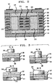
- FIG. 2 is a cross sectional view parallel to the XZ plane of the FIG. 1 device showing the individual tape layers and the spacing between regions.
- Member 201 is an insulating non-magnetic tape layer.
- Member 202 includes layers of non-magnetic tape each having an aperture within which a magnetic section 211 (shown as 101 in FIG. 1) is disposed in spaced apart relation to the insulating tape. The number of layers used to form members 202 and 211 is determined by the required magnetic cross section area.
- Members 203-207 forming the next section includes single layers of insulating non-magnetic tape having apertures for containing magnetic material sections 212 and 213 (shown as members 102 and 104 in FIG. 1).
- Members 203 through 206 contain conductor turns 214 and 216 printed on each individual layer. In this particular illustration a four turn winding is shown. It is to be understood that many added turns are possible by increasing the number of layers and by printing multiple concentric turns on each layer.
- Member 208 is similar to member 202 and includes an insulating non-magnetic tape having an aperture containing a spaced magnetic insert 218.
- the top number 209 is an insulating non-magnetic tape layer. Connector pads 221 are printed on the top surface to facilitate electrical connection to the windings.
- the result of separating the magnetic and non-magnetic green ceramics with regions of removable material is the formation of a high permeability core within the insulating ceramic but physically separated from the insulating material by a spacing regions 223 and 224. This spacing occurs because during the heat treatment, the organic binders which hold the particles in the tapes together are "burned out". During the same heat treatment, the removable tape disintegrates into vapor species and leaves the structure through the pores between the yet unsintered ceramic particles. Since, in some applications, it may be undesirable to have a completely free floating core, a plurality of small posts or tabs (not shown) of non-removable material such as either magnetic or non-magnetic ceramic material can be inserted into the removable tape to anchor the core to the insulating housing. Such posts or tabs can also provide enhanced resistance to collapse. The posts or tabs have areas which are small compared to the areas of the removable material regions in which they are placed, typically each post will be less than 5% of the area.
- FIGS. 3A and 3B illustrate a preliminary step of forming a tape of removable material containing a region of magnetic material.
- a tape of magnetic material 301 is disposed overlying a tape of removable material 302.
- the stacked layers are placed in a punch press comprising a male punch 303 in registration with a female die 304 having a recessed portion 305 with nominally the same width as the punch.
- Punch 303 is adjusted to punch the bottom of layer 301 to the bottom of layer 302.
- FIG. 3A and 3B illustrate a preliminary step of forming a tape of removable material containing a region of magnetic material.
- the stacked layers are placed in a punch press comprising a male punch 303 in registration with a female die 304 having a recessed portion 305 with nominally the same width as the punch.
- Punch 303 is adjusted to punch the bottom of layer 301 to the bottom of layer 302.
- pressure from punch 303 results in the insertion of a region 306 of magnetic material from tape 301 into the removable tape to produce a new two region tape 307.
- the corresponding region 308 of the removable tape is ejected into the recessed portion of die 304.
- the next step shown in FIGS. 3C and 3D involves inserting a portion of two-region tape 307 into a non-magnetic, insulating tape to produce a three-region tape.
- the two region tape 307 is disposed overlying a tape of non-magnetic, insulating material 309.
- a wider punch 310 with die 311 and recessed region 312 is then used to insert into layer 309 the magnetic region 306 and peripheral portions of removable material.
- the result is a multiregion tape 313 consisting of an outer region of non-magnetic material and an inner region of magnetic material separated from the non-magnetic material by removable material.
- the border of removable material preferably provides a spacing in the range 0.003-0.006 inch.
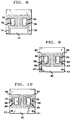
- FIG. 4 shows the bottom member as an insulating non-magnetic layer 41.
- FIG. 5 shows a top view of the next member above layer 41 and comprises an insulating non-magnetic tape 51 with an insert 52 of removable tape material.
- FIG. 6 comprises an insulating non-magnetic tape 61 with an insert 62 of magnetic material spaced from tape 61 by a peripheral layer of removable material 63.
- FIG. 7 comprises an insulating non-magnetic tape 71, a pair of magnetic inserts 73 and 74 and a region of removable material 72 disposed between the insulating material and the magnetic material.
- the next member in the structure is shown in FIG. 8 and comprises the insulating non-magnetic tape layer 701 containing magnetic inserts 705 and 706 separated from tape 701 by peripheral layers of removable material 703 and 704.
- Conductors 707 and 708 are printed onto the top surface of the tape layer 701. These conductors 707 and 708 each comprise a single turn of the transformer windings shown as windings 105 and 106 of FIG. 1. A single turn is shown surrounding each aperture; however multiple turns surrounding each aperture may be printed on each layer.
- the next structural layer shown in FIG. 9 comprises an insulating non-magnetic layer 801 having magnetic inserts 805 and 806 spaced by peripheral regions 802 and 803 of removable material.
- the conductors 807 and 808 are the second set of turns in the windings. They are connected by vias 809 and 810 to the first set of turns printed on the previous layer shown in FIG. 8.
- the vias 813 and 814 which have ring-like pads on the surface of layer 801, connect to the other ends of the windings on layer 701 and correspond to similar vias in the above layers to connect to connector pads on the top surface of the structure.
- the ring-like pads surrounding the vias are included to simplify the alignment of vias in the various layers.
- FIG. 10 shows the construction of the next member and includes an insulating non-magnetic tape layer 901 and magnetic tape inserts 904 and 905 spaced by peripheral regions 902 and 903 of removable material.
- the conductors 906 and 907 are the third set of turns in the windings and are connected by vias 908 and 909 to the second set of turns shown in FIG. 9.
- Vias 910 and 911 connect to the vias 813 and 814 in FIG. 9.
- the next member shown in FIG. 11 includes an insulating non-magnetic tape layer 1001 with two magnetic inserts 1004 and 1005 spaced by peripheral regions of removable material 1002 and 1003.
- the winding turns 1006 and 1007 are the fourth set of turns.
- Vias 1008 and 1009 connect these conductors to the conductors of the previous layer of FIG. 10.
- Vias 1010 and 1011 are part of the conductive path coupling the conductors to the bottom layer with the connector pads on the top surface of the structure. While this is the last layer including windings, it is to be understood that the number of turns is illustrative only and that the structure may contain many additional turns.
- the member illustrated in FIG. 12 includes an insulating non-magnetic layer 1101 with magnetic tape inserts 1104 and 1105 spaced by peripheral regions of removable material 1102 and 1103.
- Conducting vias 1106 and 1107 connect to the conductors shown in FIG. 11 and conducting vias 1108 and 1109 are part of the conductive path coupling the conductors of the bottom layer with the connector pads on the top surface of the structure.
- FIG. 13 is similar to FIG. 7. It includes an insulating non-magnetic layer 130 and inserts of magnetic tape 132 and 133 separated from layer 130 by a removable region 131. This member includes conducting vias 134, 135, 136 and 137 connected to corresponding vias of the adjacent members.
- FIG. 14 is similar to FIG. 6. It includes an insulating non-magnetic layer 1201 and an insert of magnetic tape 1202 spaced by peripheral region of removable material 1203. In addition, this member includes conducting vias 1204, 1205, 1206 and 1207 connected to the corresponding vias of the adjacent members.
- the member of FIG. 15 is similar to FIG. 5. It comprises an insulating non-magnetic layer 1301 and an insert of removable material 1302 to space magnetic tape 1202 of FIG. 14 from subsequent layers.
- Member 13 contains conducting vias 1304, 1305, 1306 and 1307 to connect corresponding underlying vias to the top member.
- the top member shown in FIG. 16 includes an insulating non-magnetic layer 1401 and connector pads 1402 through 1405, each containing a conductive via 1412 to 1415, respectively, which provide connection to the corresponding vias in the previous member of FIG. 15.
- the multiregion tapes shown in FIGS. 4-16 are prepared as illustrated in FIG. 3.
- Conductors having a composition compatible with the materials are printed on the layers of insulating non-magnetic green tape as needed to provide windings, and the successive layers are stacked in registration.
- the stacked structure is laminated under low pressure (500 - 3000 psi) at a temperature of 40 to 80°C, and the laminated structure is fired (sintered) at a temperature between 800 and 1500°C to form the resulting composite structure of the magnetic component.
- the removable material disintegrates, leaving the structure as volatile species.
- the residual precise spacing between the two types of constituent ceramic material alleviates fabrication problems due to different thermal characteristics of the two materials, thereby reducing cracking and degradation due to magnetostriction.
- FIG. 3 An alternative application of the process shown in FIG. 3 to the fabrication of magnetic devices concerns the formation of conductive elements such as vias 108 and windings 105 of FIG. 1.
- conductive elements such as vias 108 and windings 105 of FIG. 1.
- removable material inserts would be substituted for conductive ink as elements 707 and 708 of FIG. 8, elements 807, 808, 809, 810, 813 and 814 of FIG. 9, elements 906 through 911 of FIG. 10, elements 1006 through 1011 of FIG. 11, elements 1106 through 1109 of FIG.
- voids are intentionally open to the surface so that they can then be filled with low melting temperature metal, such as solder, by immersing the structure in a molten bath to fill the empty spaces. After immersion, a vacuum can be drawn over the bath to remove gases in the helical voids and, subsequently, pressure can be applied to the bath to ensure the flow of metal into the voids.
- low melting temperature metal such as solder
Landscapes
- Engineering & Computer Science (AREA)
- Manufacturing & Machinery (AREA)
- Chemical & Material Sciences (AREA)
- Ceramic Engineering (AREA)
- Mechanical Engineering (AREA)
- Power Engineering (AREA)
- Coils Or Transformers For Communication (AREA)
- Manufacturing Cores, Coils, And Magnets (AREA)
Applications Claiming Priority (2)
| Application Number | Priority Date | Filing Date | Title |
|---|---|---|---|
| US07/818,669 US5239744A (en) | 1992-01-09 | 1992-01-09 | Method for making multilayer magnetic components |
| US818669 | 1992-01-09 |
Publications (3)
| Publication Number | Publication Date |
|---|---|
| EP0550974A2 true EP0550974A2 (fr) | 1993-07-14 |
| EP0550974A3 EP0550974A3 (en) | 1993-08-25 |
| EP0550974B1 EP0550974B1 (fr) | 2001-05-16 |
Family
ID=25226114
Family Applications (1)
| Application Number | Title | Priority Date | Filing Date |
|---|---|---|---|
| EP92311246A Expired - Lifetime EP0550974B1 (fr) | 1992-01-09 | 1992-12-10 | Méthode pour la fabrication de composants magnétiques multicouches |
Country Status (4)
| Country | Link |
|---|---|
| US (1) | US5239744A (fr) |
| EP (1) | EP0550974B1 (fr) |
| JP (1) | JP2607023B2 (fr) |
| DE (1) | DE69231827T2 (fr) |
Cited By (4)
| Publication number | Priority date | Publication date | Assignee | Title |
|---|---|---|---|---|
| EP0601779A1 (fr) * | 1992-12-08 | 1994-06-15 | AT&T Corp. | Composants céramiques frittés améliorés et leur procédé de fabrication |
| EP1791139A1 (fr) * | 2005-11-25 | 2007-05-30 | Zarlink Semiconductor Limited | Composant inductif |
| CN103489622A (zh) * | 2012-06-08 | 2014-01-01 | 胜美达集团株式会社 | 磁性元件的制造方法及磁性元件 |
| EP3460812A4 (fr) * | 2016-05-16 | 2019-11-06 | Moda-Innochips Co., Ltd. | Élément de protection de circuit |
Families Citing this family (26)
| Publication number | Priority date | Publication date | Assignee | Title |
|---|---|---|---|---|
| JP3099500B2 (ja) * | 1992-01-31 | 2000-10-16 | 株式会社村田製作所 | 複合積層トランス及びその製造方法 |
| US5690771A (en) * | 1993-03-31 | 1997-11-25 | Taiyo Yuden Kabushiki Kaisha | Electronic parts such as an inductor and method for making same |
| TW265450B (en) | 1994-06-30 | 1995-12-11 | At & T Corp | Devices using metallized magnetic substrates |
| US5619791A (en) * | 1994-06-30 | 1997-04-15 | Lucent Technologies Inc. | Method for fabricating highly conductive vias |
| DE69531980T2 (de) * | 1994-08-23 | 2004-07-29 | At & T Corp. | Metallisierung von keramischen Materialien durch Auftrag einer haftenden reduzierbaren Schicht |
| US5661882A (en) * | 1995-06-30 | 1997-09-02 | Ferro Corporation | Method of integrating electronic components into electronic circuit structures made using LTCC tape |
| AT1045U1 (de) * | 1995-10-03 | 1996-09-25 | Fronius Schweissmasch | Spulenkörper und verfahren zu dessen herstellung für einen transformator |
| US5787569A (en) * | 1996-02-21 | 1998-08-04 | Lucent Technologies Inc. | Encapsulated package for power magnetic devices and method of manufacture therefor |
| US6007758A (en) * | 1998-02-10 | 1999-12-28 | Lucent Technologies Inc. | Process for forming device comprising metallized magnetic substrates |
| JP3621300B2 (ja) * | 1999-08-03 | 2005-02-16 | 太陽誘電株式会社 | 電源回路用積層インダクタ |
| JP2001044037A (ja) * | 1999-08-03 | 2001-02-16 | Taiyo Yuden Co Ltd | 積層インダクタ |
| US6306677B1 (en) * | 2000-03-07 | 2001-10-23 | Delphi Technologies, Inc. | Method and apparatus for punch and place inserts for manufacture of oxygen sensor |
| US7018494B2 (en) * | 2002-08-28 | 2006-03-28 | Kyocera Corporation | Method of producing a composite sheet and method of producing a laminate by using the composite sheet |
| JP2004265898A (ja) * | 2003-01-21 | 2004-09-24 | Tdk Corp | 多層セラミック基板およびその製造方法 |
| JP4071204B2 (ja) | 2004-02-27 | 2008-04-02 | Tdk株式会社 | 多層セラミック基板の製造方法 |
| JP4454390B2 (ja) * | 2004-05-27 | 2010-04-21 | 京セラ株式会社 | グリーンシート積層体、およびセラミック構造体の製造方法 |
| WO2010035559A1 (fr) * | 2008-09-24 | 2010-04-01 | 株式会社村田製作所 | Composant en bobine stratifié |
| US10049799B2 (en) * | 2012-05-10 | 2018-08-14 | Emw Co., Ltd. | Magnetic sheet, method for manufacturing magnetic sheet and antenna comprising the magnetic sheet |
| KR20160032581A (ko) * | 2014-09-16 | 2016-03-24 | 삼성전기주식회사 | 인덕터 어레이 칩 및 그 실장기판 |
| US10468181B1 (en) * | 2015-08-10 | 2019-11-05 | Vlt, Inc. | Self-aligned planar magnetic structure and method |
| US10128764B1 (en) | 2015-08-10 | 2018-11-13 | Vlt, Inc. | Method and apparatus for delivering power to semiconductors |
| US12525885B1 (en) | 2016-04-05 | 2026-01-13 | Vicor Corporation | Planar inductive apparatus and method |
| KR101843260B1 (ko) * | 2016-05-30 | 2018-03-28 | 삼성전기주식회사 | 칩 인덕터 및 그의 제조 방법 |
| US11373803B2 (en) | 2017-08-11 | 2022-06-28 | Applied Materials, Inc. | Method of forming a magnetic core on a substrate |
| WO2019059897A1 (fr) * | 2017-09-20 | 2019-03-28 | Intel Corporation | Ensembles bobine d'inductance/noyau pour circuits intégrés |
| US12336118B1 (en) | 2020-05-19 | 2025-06-17 | Vicor Corporation | Planar inductive apparatus and method |
Citations (2)
| Publication number | Priority date | Publication date | Assignee | Title |
|---|---|---|---|---|
| DE3628021A1 (de) | 1986-08-19 | 1988-02-25 | Siemens Ag | Chip-bauteil mit wenigstens einer spule und verfahren zu dessen herstellung |
| US5349743A (en) | 1991-05-02 | 1994-09-27 | At&T Bell Laboratories | Method of making a multilayer monolithic magnet component |
Family Cites Families (13)
| Publication number | Priority date | Publication date | Assignee | Title |
|---|---|---|---|---|
| GB1041315A (en) * | 1964-08-26 | 1966-09-01 | Ass Elect Ind | Manufacture of ferrite plate |
| US3768144A (en) * | 1971-03-04 | 1973-10-30 | American Lava Corp | Process for ceramic composites |
| US3965552A (en) * | 1972-07-24 | 1976-06-29 | N L Industries, Inc. | Process for forming internal conductors and electrodes |
| US4301580A (en) * | 1977-04-16 | 1981-11-24 | Wallace Clarence L | Manufacture of multi-layered electrical assemblies |
| GB2103422B (en) * | 1981-07-30 | 1985-02-27 | Standard Telephones Cables Ltd | Ceramic capacitors |
| US4584629A (en) * | 1984-07-23 | 1986-04-22 | Avx Corporation | Method of making ceramic capacitor and resulting article |
| JPS61193418A (ja) * | 1985-02-21 | 1986-08-27 | 株式会社村田製作所 | 積層セラミツクコンデンサ |
| ATE82086T1 (de) * | 1986-08-18 | 1992-11-15 | Siemens Ag | Fuellschichtbauteil. |
| ES2023384B3 (es) * | 1986-08-18 | 1992-01-16 | Siemens Ag | Procedimiento para preparar componentes de capas de relleno |
| EP0260427A1 (fr) * | 1986-08-18 | 1988-03-23 | Siemens Aktiengesellschaft | Composant à couches imprégnées et son procédé de fabrication |
| DE3725454A1 (de) * | 1987-07-31 | 1989-02-09 | Siemens Ag | Elektrisches vielschichtbauelement mit einem gesinterten, monolithischen keramikkoerper und verfahren zur herstellung des elektrischen vielschichtbauelementes |
| JPH02172207A (ja) * | 1988-12-23 | 1990-07-03 | Murata Mfg Co Ltd | 積層型インダクター |
| JPH05174649A (ja) * | 1991-12-24 | 1993-07-13 | Tdk Corp | 異質材部を有するセラミックグリーンシート及びその製造方法 |
-
1992
- 1992-01-09 US US07/818,669 patent/US5239744A/en not_active Expired - Fee Related
- 1992-12-10 DE DE69231827T patent/DE69231827T2/de not_active Expired - Fee Related
- 1992-12-10 EP EP92311246A patent/EP0550974B1/fr not_active Expired - Lifetime
-
1993
- 1993-01-11 JP JP5017891A patent/JP2607023B2/ja not_active Expired - Fee Related
Patent Citations (2)
| Publication number | Priority date | Publication date | Assignee | Title |
|---|---|---|---|---|
| DE3628021A1 (de) | 1986-08-19 | 1988-02-25 | Siemens Ag | Chip-bauteil mit wenigstens einer spule und verfahren zu dessen herstellung |
| US5349743A (en) | 1991-05-02 | 1994-09-27 | At&T Bell Laboratories | Method of making a multilayer monolithic magnet component |
Cited By (6)
| Publication number | Priority date | Publication date | Assignee | Title |
|---|---|---|---|---|
| EP0601779A1 (fr) * | 1992-12-08 | 1994-06-15 | AT&T Corp. | Composants céramiques frittés améliorés et leur procédé de fabrication |
| US5389428A (en) * | 1992-12-08 | 1995-02-14 | At&T Corp. | Sintered ceramic components and method for making same |
| EP1791139A1 (fr) * | 2005-11-25 | 2007-05-30 | Zarlink Semiconductor Limited | Composant inductif |
| CN103489622A (zh) * | 2012-06-08 | 2014-01-01 | 胜美达集团株式会社 | 磁性元件的制造方法及磁性元件 |
| CN103489622B (zh) * | 2012-06-08 | 2016-02-03 | 胜美达集团株式会社 | 磁性元件的制造方法及磁性元件 |
| EP3460812A4 (fr) * | 2016-05-16 | 2019-11-06 | Moda-Innochips Co., Ltd. | Élément de protection de circuit |
Also Published As
| Publication number | Publication date |
|---|---|
| EP0550974A3 (en) | 1993-08-25 |
| JP2607023B2 (ja) | 1997-05-07 |
| DE69231827D1 (de) | 2001-06-21 |
| US5239744A (en) | 1993-08-31 |
| EP0550974B1 (fr) | 2001-05-16 |
| DE69231827T2 (de) | 2001-11-22 |
| JPH0684675A (ja) | 1994-03-25 |
Similar Documents
| Publication | Publication Date | Title |
|---|---|---|
| US5239744A (en) | Method for making multilayer magnetic components | |
| US5479695A (en) | Method of making a multilayer monolithic magnetic component | |
| US6094123A (en) | Low profile surface mount chip inductor | |
| US5802702A (en) | Method of making a device including a metallized magnetic substrate | |
| US7295092B2 (en) | Gapped core structure for magnetic components | |
| KR101994722B1 (ko) | 적층형 전자부품 | |
| KR101433838B1 (ko) | 인덕티브 구성요소 및 상기 인덕티브 구성요소를 제조하기 위한 방법 | |
| JP2004500693A (ja) | コア及び巻線構造及びその製造方法 | |
| US4731297A (en) | Laminated components of open magnetic circuit type | |
| JPH08130109A (ja) | 積層部品用非磁性絶縁材料、積層部品およびその製造法 | |
| JPS59132604A (ja) | 積層型インダクタ | |
| JPH05121240A (ja) | インダクタンス部品およびその製造方法 | |
| JP2604022Y2 (ja) | 積層セラミックインダクタ | |
| JPH09199331A (ja) | コイル部品およびその製造方法 | |
| KR0173240B1 (ko) | 전자기적 특성이 양호한 인덕터 칩의 제조방법 | |
| JP2001135548A (ja) | 電子部品およびその製造方法 | |
| JPH09199333A (ja) | コイル部品およびその製造方法 | |
| JPH0590029A (ja) | 積層型コイル及びその製造方法 | |
| JPH08236409A (ja) | 積層複合部品およびその製造方法 | |
| JPH09260142A (ja) | コイル部品およびその製造方法 | |
| JPH09275014A (ja) | コイル部品およびその製造方法 | |
| JPH09190925A (ja) | コイル部品およびその製造方法 | |
| JPH1027718A (ja) | コイル部品およびその製造方法 | |
| JPH09283336A (ja) | 積層型複合インダクタ | |
| JPH09186020A (ja) | コイル部品およびその製造方法 |
Legal Events
| Date | Code | Title | Description |
|---|---|---|---|
| PUAI | Public reference made under article 153(3) epc to a published international application that has entered the european phase |
Free format text: ORIGINAL CODE: 0009012 |
|
| PUAL | Search report despatched |
Free format text: ORIGINAL CODE: 0009013 |
|
| AK | Designated contracting states |
Kind code of ref document: A2 Designated state(s): DE FR GB |
|
| AK | Designated contracting states |
Kind code of ref document: A3 Designated state(s): DE FR GB |
|
| 17P | Request for examination filed |
Effective date: 19940210 |
|
| RAP3 | Party data changed (applicant data changed or rights of an application transferred) |
Owner name: AT&T CORP. |
|
| 17Q | First examination report despatched |
Effective date: 19950828 |
|
| APAB | Appeal dossier modified |
Free format text: ORIGINAL CODE: EPIDOS NOAPE |
|
| APAB | Appeal dossier modified |
Free format text: ORIGINAL CODE: EPIDOS NOAPE |
|
| APAD | Appeal reference recorded |
Free format text: ORIGINAL CODE: EPIDOS REFNE |
|
| APCB | Communication from the board of appeal sent |
Free format text: ORIGINAL CODE: EPIDOS OBAPE |
|
| APCB | Communication from the board of appeal sent |
Free format text: ORIGINAL CODE: EPIDOS OBAPE |
|
| APAB | Appeal dossier modified |
Free format text: ORIGINAL CODE: EPIDOS NOAPE |
|
| GRAG | Despatch of communication of intention to grant |
Free format text: ORIGINAL CODE: EPIDOS AGRA |
|
| GRAH | Despatch of communication of intention to grant a patent |
Free format text: ORIGINAL CODE: EPIDOS IGRA |
|
| GRAH | Despatch of communication of intention to grant a patent |
Free format text: ORIGINAL CODE: EPIDOS IGRA |
|
| GRAA | (expected) grant |
Free format text: ORIGINAL CODE: 0009210 |
|
| AK | Designated contracting states |
Kind code of ref document: B1 Designated state(s): DE FR GB |
|
| REF | Corresponds to: |
Ref document number: 69231827 Country of ref document: DE Date of ref document: 20010621 |
|
| ET | Fr: translation filed | ||
| PG25 | Lapsed in a contracting state [announced via postgrant information from national office to epo] |
Ref country code: GB Free format text: LAPSE BECAUSE OF NON-PAYMENT OF DUE FEES Effective date: 20011210 |
|
| REG | Reference to a national code |
Ref country code: GB Ref legal event code: IF02 |
|
| PLBE | No opposition filed within time limit |
Free format text: ORIGINAL CODE: 0009261 |
|
| 26N | No opposition filed | ||
| PG25 | Lapsed in a contracting state [announced via postgrant information from national office to epo] |
Ref country code: DE Free format text: LAPSE BECAUSE OF NON-PAYMENT OF DUE FEES Effective date: 20020702 |
|
| GBPC | Gb: european patent ceased through non-payment of renewal fee |
Effective date: 20011210 |
|
| PG25 | Lapsed in a contracting state [announced via postgrant information from national office to epo] |
Ref country code: FR Free format text: LAPSE BECAUSE OF NON-PAYMENT OF DUE FEES Effective date: 20020830 |
|
| REG | Reference to a national code |
Ref country code: FR Ref legal event code: ST |
|
| APAH | Appeal reference modified |
Free format text: ORIGINAL CODE: EPIDOSCREFNO |