EP0553733A2 - Appareil électronique et procédé de modification d'une information fixe - Google Patents
Appareil électronique et procédé de modification d'une information fixe Download PDFInfo
- Publication number
- EP0553733A2 EP0553733A2 EP93101008A EP93101008A EP0553733A2 EP 0553733 A2 EP0553733 A2 EP 0553733A2 EP 93101008 A EP93101008 A EP 93101008A EP 93101008 A EP93101008 A EP 93101008A EP 0553733 A2 EP0553733 A2 EP 0553733A2
- Authority
- EP
- European Patent Office
- Prior art keywords
- address
- patch
- program
- patching
- interrupt
- Prior art date
- Legal status (The legal status is an assumption and is not a legal conclusion. Google has not performed a legal analysis and makes no representation as to the accuracy of the status listed.)
- Granted
Links
Images

Classifications
-
- G—PHYSICS
- G06—COMPUTING OR CALCULATING; COUNTING
- G06F—ELECTRIC DIGITAL DATA PROCESSING
- G06F8/00—Arrangements for software engineering
- G06F8/60—Software deployment
- G06F8/65—Updates
- G06F8/66—Updates of program code stored in read-only memory [ROM]
-
- G—PHYSICS
- G06—COMPUTING OR CALCULATING; COUNTING
- G06F—ELECTRIC DIGITAL DATA PROCESSING
- G06F11/00—Error detection; Error correction; Monitoring
- G06F11/07—Responding to the occurrence of a fault, e.g. fault tolerance
- G06F11/08—Error detection or correction by redundancy in data representation, e.g. by using checking codes
-
- G—PHYSICS
- G06—COMPUTING OR CALCULATING; COUNTING
- G06F—ELECTRIC DIGITAL DATA PROCESSING
- G06F9/00—Arrangements for program control, e.g. control units
- G06F9/06—Arrangements for program control, e.g. control units using stored programs, i.e. using an internal store of processing equipment to receive or retain programs
- G06F9/30—Arrangements for executing machine instructions, e.g. instruction decode
- G06F9/32—Address formation of the next instruction, e.g. by incrementing the instruction counter
- G06F9/322—Address formation of the next instruction, e.g. by incrementing the instruction counter for non-sequential address
- G06F9/328—Address formation of the next instruction, e.g. by incrementing the instruction counter for non-sequential address for runtime instruction patching
-
- G—PHYSICS
- G06—COMPUTING OR CALCULATING; COUNTING
- G06F—ELECTRIC DIGITAL DATA PROCESSING
- G06F9/00—Arrangements for program control, e.g. control units
- G06F9/06—Arrangements for program control, e.g. control units using stored programs, i.e. using an internal store of processing equipment to receive or retain programs
- G06F9/30—Arrangements for executing machine instructions, e.g. instruction decode
- G06F9/38—Concurrent instruction execution, e.g. pipeline or look ahead
- G06F9/3861—Recovery, e.g. branch miss-prediction, exception handling
Definitions
- the present invention relates to an electronic apparatus such as a one-chip microcomputer incorporated within electronic devices, for example.
- a one-chip microcomputer incorporated within electronic devices is formed of an electronic apparatus in which a fixed memory means (ROM (read only memory)), a processing means (CPU (central processing unit)), an input means, a variable memory means (RAM (random access memory)), etc., are unitarily integrated.
- ROM read only memory
- CPU central processing unit
- RAM random access memory
- a program for the processing in the processing means (CPU) is stored in the fixed memory means (ROM), for example. That is, a particular processing is executed in accordance with an information (processing program) stored in the fixed memory means (ROM).
- ROM fixed memory means
- Such fixed memory means is formed of, for example, a mask-ROM, then such electronic apparatus can be made inexpensively by means of mass-production.
- the above electronic apparatus are incorporated within electronic devices such as a consumer VTR (video tape recorder) having a built-in camera, a compact video deck or the like.
- electronic devices such as a consumer VTR (video tape recorder) having a built-in camera, a compact video deck or the like.
- the electronic devices are so designed as to have multiple functions in order to discriminate products.
- the amount of information (processing program) stored in the fixed memory means (ROM) is increased and, particularly, the processing program becomes extremely long, which unavoidably causes a defect (bug) to occur.
- a patch information memory means for patching a bug in the electronic apparatus, there are provided a patch information memory means for patching a bug and an access switching means. A bug portion is discriminated on the basis of an information stored in a fixed memory means. At that bug portion, the memory access is switched from the fixed memory means to the patch information memory means.
- an electronic apparatus which comprises a fixed memory means in which an information is stored in a fixed fashion, an address control means for controlling an address, an input means through which an external information is input, a patch information memory means for storing therein a patch information concerning a portion to be changed in the information stored in the fixed memory means, and a switching control means for switching the memory access made by the address control means from the fixed memory means to the patch information memory means.
- the address control means includes a first memory in which there is saved control data for controlling the switching of memory access by the address control means when an interrupt processing is executed so that the control data for controlling the switching of the memory access during the interrupt processing can be set in the switching control means.
- the fixed memory means, the address control means, the input means, the patch information memory means and the switching control means being unitarily integrated in the electronic apparatus
- a fixed information patching method for operation of an electronic apparatus which comprises fixed memory means in which an information is stored in a fixed fashion, address control means for controlling an address, input means through which an external information is input, patch information memory means for storing therein a patch information concerning a portion to be changed in the information stored in the fixed memory means, and switching control means for switching the memory access made by the address control means from the fixed memory means to the patch information memory means at a predetermined address.
- This method comprises the steps of saving the control data for controlling the switching of the memory access by the address control means to a first memory during the beginning of an interrupt processing to the address control means, and setting the control data for controlling the switching of the memory access during the interrupt processing in the switching control means.
- the fixed memory means, the address control means, the input means, the patch information memory means and the switching control means are unitarily integrated in the electronic apparatus.
- the information stored in the fixed memory means is patched by the information from the patch information memory means and the information bug that is discovered after electronic devices were mass-produced can be patched. Also, by saving discriminating data of the patch portion to a stack memory, a bug can be patched during the interrupt processing.
- reference numeral 10 generally designates a one-chip microcomputer serving as an electronic apparatus.
- the electronic apparatus 10 includes a CPU (central processing unit) 1 serving as a processing means, a ROM (read only memory) 2 serving as a fixed memory means, a RAM (random access memory) 3 serving as a patch information memory means, an input means 4, e.g. an input/output (I/O) port or the like.
- the CPU 1, ROM 2, the RAM 3 and the input means 4 are connected to one another via a data bus 5.
- An address output formed by the CPU 1 is supplied through an address bus 6 to the address inputs of the ROM 2 and the RAM 3.
- the CPU 1 includes also interrupt control portions A, B, C, ... for other processing.
- An external storage device 20 is connected to the input means 4.
- the external storage device 20 also is incorporated within the electronic device.
- the external storage device 20 is formed of an EEPROM (electrically erasable and programmable ROM) in which there are generally stored parameters obtained in the adjustment process of electronic device, etc.
- An information from the external storage device 20 is supplied through the input means 4 and then stored in the RAM 4, thereby being utilized in the processing done by the CPU 1.
- a program information for the processing in the CPU 1 is stored in the ROM 2 in a fixed fashion.
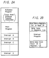
- an activation program shown in FIG. 2A for example.
- the activation program includes a program for initializing the apparatus such as when the RAM 3 is cleared, and a program for transferring the information from the external storage device 20 through the input means 4 to the RAM 3 or the like.
- a main program for executing a main processing and interrupt programs for executing a variety of interruptions A, B, C, ...
- a processing program which writes into the registers 7 and 8, respectively, from the fixed table area 31 of the RAM 3, an address of a first bug portion written in the RAM 3 and vector data representative of a starting position of the patch program for patching the first bug portion.
- each interrupt program As shown in FIG. 2B, there is provided a processing in which data written in the registers 7 and 8 are saved in the RAM 3 at its stack area 32 which will be described later on. This processing is followed by a processing in which an address of a first patching portion corresponding to the interrupt and vector data representative of a starting position of a patch program for patching the bug portion of the interrupt are written in the registers 7 and 8, respectively. At the end of the interrupt program, there is provided a processing in which the data saved in the stack area 32 is written again in the registers 7 and 8.
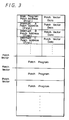
- the external storage device 20 there are stored information used to patch a bug in the information stored in the ROM 2, together with the parameters obtained in the previously described adjustment process.
- the information used to patch the bug is shown in FIG. 3 and includes an address of a first bug portion corresponding to the main program and the interrupt, vector data representative of a starting position a patch program for patching the first bug portion, and the patch program.
- the information from the external storage device 20 is stored in the RAM 3 through the input means 4.
- the patch program is stored in a patch program portion of the RAM 3.
- the main program, the address of the first bug portion corresponding to the interrupt and vector data representative of the starting position of the patch program for patching the first bug portion are written in the fixed table area 31 of the RAM 3.
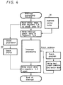
- the address of the first bug portion in the main program and vector data representative of the starting position of the patch program for patching the first bug portion are read out from the fixed table area 31 of the RAM 3 and then written in the registers 7 and 8. Then, when the main program proceeds and the address thereof becomes coincident with the address of the register 7, a signal is supplied to the interrupt control portion X of the CPU 1.
- data of the register 8 is referred to by the CPU 1 in processing of the interrupt control portion X, and a patch program located at the position indicated by the above data is executed. Further, at the end of this patch program, there are provided an address of the next patch portion of the interrupt program, vector data representative of the starting position of the patch program for patching the address, and a processing by which they are written in the registers 7 and 8, respectively. As described above, the patch portions of the main programs are patched sequentially.
- the respective interrupt processings A, B, C, ... are executed.
- data written in the registers 7 and 8 are saved in the stack area 32 of the RAM 3.
- the first patch portion address corresponding to the above interruption and the vector data representative of the starting position of the patch program for patching the address of the patch portion are read out from the fixed table area 31 of the RAM 3 and then written in the registers 7 and 8.
- the interrupt program proceeds and the address becomes coincident with the address of the register 7, then a signal is supplied to the interrupt control portion X of the CPU 1.
- the data in the register 8 is referred to by the CPU 1 for the interrupt processing and then the patch program at the position indicated by that data is executed. Further, at the end of this patch program, there are provided an address of the next patch portion in the interrupt program and vector data representative of the starting position of the patch program for patching the address, and a processing by which they are written in the registers 7 and 8, respectively. In this way, the patch portions of the interrupt programs are sequentially patched. Furthermore, at the end of this interrupt program, data saved in the stack area 32 are written in the registers 7 and 8 one more time.
- the address of the patching portion of the main program and the vector data representative of the starting position of the patch program for patching the address are saved from the registers 7 and 8 to the stack area 32.
- the address of the first patch portion corresponding to the above interrupt and the vector data representative of the starting position of the patch program for patching the address are read out from the fixed table area 31 of the RAM 3 and written in the registers 7 and 8.
- the patch portions of the interrupt programs are patched sequentially.
- the data saved in the stack area 32 are again written in the registers 7 and 8, whereby the patching process of the patch portions in the main program is continuously executed.
- the information stored in the fixed memory means (ROM 2) is patched by the information from the patch information memory means (RAM 3) and the information bug that is discovered when the electronic device was mass-produced can be patched. Also, by saving the discriminating data of the patch information to the stack memory (stack area 32), the bug can be patched during the interrupt.
- the stack area 32 may be arranged as a so-called pushdown stack. If so, then the electronic apparatus of the present invention can be applied to a multiple interrupt in which an interrupt is executed during an interrupt.
- the switching means for switching the memory access from the ROM 2 to the RAM 3 may be modified such that the vector data representative of the starting position of the patch program is replaced with a jump command to that position and the output data of the ROM 2 and the data in the register 8 is switched when the addresses compared by the comparator 9 become coincident with each other.
- address data of the first patch portion corresponding to the interrupt is stored in the fixed table area 31 of the RAM 3 at every processing of various interrupts A, B, C, ... If there is no bug portion in an arbitrary interrupt processing, then corresponding data in the fixed table area 31 must be written in the fixed table area 31 by selecting an address which is not accessed during the interrupt processing.
- the information stored in the fixed memory means is patched by the information from the patch information memory means and the information bug that is discovered after electronic devices were mass-produced can be patched. Also, by saving the discriminating data of the patch portion into the stack memory, a bug can be patched during the interrupt processing.
Landscapes
- Engineering & Computer Science (AREA)
- Theoretical Computer Science (AREA)
- Software Systems (AREA)
- General Engineering & Computer Science (AREA)
- Physics & Mathematics (AREA)
- General Physics & Mathematics (AREA)
- Computer Security & Cryptography (AREA)
- Quality & Reliability (AREA)
- Debugging And Monitoring (AREA)
- Stored Programmes (AREA)
- Storage Device Security (AREA)
Applications Claiming Priority (3)
| Application Number | Priority Date | Filing Date | Title |
|---|---|---|---|
| JP11206/92 | 1992-01-24 | ||
| JP1120692 | 1992-01-24 | ||
| JP01120692A JP3230262B2 (ja) | 1992-01-24 | 1992-01-24 | 電子装置及びその固定情報修正方法 |
Publications (3)
| Publication Number | Publication Date |
|---|---|
| EP0553733A2 true EP0553733A2 (fr) | 1993-08-04 |
| EP0553733A3 EP0553733A3 (en) | 1997-10-15 |
| EP0553733B1 EP0553733B1 (fr) | 2001-12-12 |
Family
ID=11771541
Family Applications (1)
| Application Number | Title | Priority Date | Filing Date |
|---|---|---|---|
| EP93101008A Expired - Lifetime EP0553733B1 (fr) | 1992-01-24 | 1993-01-22 | Appareil électronique et procédé de modification d'une information fixe |
Country Status (6)
| Country | Link |
|---|---|
| US (1) | US6128751A (fr) |
| EP (1) | EP0553733B1 (fr) |
| JP (1) | JP3230262B2 (fr) |
| KR (1) | KR100307857B1 (fr) |
| CA (1) | CA2087696A1 (fr) |
| DE (1) | DE69331292T2 (fr) |
Cited By (11)
| Publication number | Priority date | Publication date | Assignee | Title |
|---|---|---|---|---|
| GB2292470A (en) * | 1994-08-19 | 1996-02-21 | Advanced Risc Mach Ltd | Rom patching |
| GB2309324A (en) * | 1996-01-17 | 1997-07-23 | Motorola Inc | Method for storing repair data in a microprocessor |
| EP0688138A3 (fr) * | 1994-06-15 | 1997-08-20 | Nec Corp | Récepteur d'appels sélectifs |
| EP0871125A1 (fr) * | 1997-04-08 | 1998-10-14 | AITM Associates, Incorporated | Module logique pour des changements du système dans un ordinateur à architecture de type PC |
| EP0883062A1 (fr) * | 1997-06-05 | 1998-12-09 | Alcatel | Dispositif de retouche de programme de commande dans un processeur |
| EP1111510A1 (fr) * | 1999-12-24 | 2001-06-27 | Matsushita Electric Industrial Co., Ltd. | Dispositif de modification de programmes |
| EP0817013A3 (fr) * | 1996-06-28 | 2003-07-16 | NEC Electronics Corporation | Méthode et dispositif de traitement de données |
| US7305712B2 (en) | 2002-11-18 | 2007-12-04 | Arm Limited | Security mode switching via an exception vector |
| CN100504784C (zh) * | 2006-02-17 | 2009-06-24 | 国际商业机器公司 | 用于可选只读存储器表征的方法和装置 |
| US7849310B2 (en) | 2002-11-18 | 2010-12-07 | Arm Limited | Switching between secure and non-secure processing modes |
| CN103268237A (zh) * | 2013-05-10 | 2013-08-28 | 东信和平科技股份有限公司 | 一种掩膜智能卡的补丁功能扩展方法及装置 |
Families Citing this family (14)
| Publication number | Priority date | Publication date | Assignee | Title |
|---|---|---|---|---|
| JP2001256044A (ja) * | 2000-03-14 | 2001-09-21 | Sony Corp | データ処理装置 |
| GB2373888A (en) * | 2001-03-30 | 2002-10-02 | Toshiba Res Europ Ltd | Dynamic vector address allocation for a code patching scheme |
| US20040015939A1 (en) * | 2001-05-16 | 2004-01-22 | Cheah Jonathon Y. | Updateable memory module |
| US6925521B2 (en) * | 2001-09-10 | 2005-08-02 | Texas Instruments Incorporated | Scheme for implementing breakpoints for on-chip ROM code patching |
| JP2004213102A (ja) * | 2002-12-26 | 2004-07-29 | Fujitsu Ltd | マイクロコンピュータ |
| US7269707B2 (en) * | 2003-01-10 | 2007-09-11 | Texas Instruments Incorporated | Multiple patches to on-chip ROM in a processor with a multilevel memory system without affecting performance |
| US7596721B1 (en) * | 2004-01-09 | 2009-09-29 | Maxtor Corporation | Methods and structure for patching embedded firmware |
| US7464248B2 (en) | 2005-04-25 | 2008-12-09 | Mediatek Incorporation | Microprocessor systems and bus address translation methods |
| US7533240B1 (en) * | 2005-06-01 | 2009-05-12 | Marvell International Ltd. | Device with mapping between non-programmable and programmable memory |
| EP1983429A1 (fr) * | 2007-04-19 | 2008-10-22 | Proton World International N.V. | Implémentation de programmes correctifs par une unité de traitement |
| CN101334760B (zh) * | 2007-06-26 | 2010-04-07 | 展讯通信(上海)有限公司 | 监控总线非法操作的方法、装置及包含该装置的系统 |
| US8156486B2 (en) * | 2008-10-29 | 2012-04-10 | Mediatek Inc. | Patching devices and methods thereof for patching firmware functions |
| US9547489B2 (en) * | 2014-03-31 | 2017-01-17 | Qualcomm Incorporated | System and method for modifying a sequence of instructions in a read-only memory of a computing device |
| CN116302627B (zh) * | 2022-09-09 | 2025-09-19 | 珠海市杰理科技股份有限公司 | 一种嵌入式设备及rom程序的修复方法 |
Family Cites Families (51)
| Publication number | Priority date | Publication date | Assignee | Title |
|---|---|---|---|---|
| US4150428A (en) * | 1974-11-18 | 1979-04-17 | Northern Electric Company Limited | Method for providing a substitute memory in a data processing system |
| JPS5721799B2 (fr) * | 1975-02-01 | 1982-05-10 | ||
| JPS5245232A (en) * | 1975-10-08 | 1977-04-09 | Hitachi Ltd | Micro program modification circuit |
| US4028684A (en) * | 1975-10-16 | 1977-06-07 | Bell Telephone Laboratories, Incorporated | Memory patching circuit with repatching capability |
| US4028683A (en) * | 1975-10-16 | 1977-06-07 | Bell Telephone Laboratories, Incorporated | Memory patching circuit with counter |
| US4028678A (en) * | 1975-10-16 | 1977-06-07 | Bell Telephone Laboratories, Incorporated | Memory patching circuit |
| US4218757A (en) * | 1978-06-29 | 1980-08-19 | Burroughs Corporation | Device for automatic modification of ROM contents by a system selected variable |
| US4291375A (en) * | 1979-03-30 | 1981-09-22 | Westinghouse Electric Corp. | Portable programmer-reader unit for programmable time registering electric energy meters |
| US4296470A (en) * | 1979-06-21 | 1981-10-20 | International Business Machines Corp. | Link register storage and restore system for use in an instruction pre-fetch micro-processor interrupt system |
| JPS56136054A (en) * | 1980-03-26 | 1981-10-23 | Hitachi Ltd | Function assigning circuit |
| US4319343A (en) * | 1980-07-16 | 1982-03-09 | Honeywell Inc. | Programmable digital memory circuit |
| US4456966A (en) * | 1981-02-26 | 1984-06-26 | International Business Machines Corporation | Memory system with flexible replacement units |
| JPS57150019A (en) * | 1981-03-13 | 1982-09-16 | Hitachi Ltd | Control system of terminal device |
| JPS57196357A (en) * | 1981-05-29 | 1982-12-02 | Toshiba Corp | Data processor |
| JPS57211651A (en) * | 1981-06-23 | 1982-12-25 | Toshiba Corp | Patch system |
| US4490783A (en) * | 1981-07-02 | 1984-12-25 | Texas Instruments Incorporated | Microcomputer with self-test of microcode |
| US4400798A (en) * | 1981-07-13 | 1983-08-23 | Tektronix, Inc. | Memory patching system |
| JPS5816350A (ja) * | 1981-07-22 | 1983-01-31 | Toshiba Corp | メモリ拡張代替方式 |
| JPS5886648A (ja) * | 1981-11-18 | 1983-05-24 | Mitsubishi Electric Corp | トレ−ス装置 |
| US4542453A (en) * | 1982-02-19 | 1985-09-17 | Texas Instruments Incorporated | Program patching in microcomputer |
| US4490812A (en) * | 1982-09-30 | 1984-12-25 | Mostek Corporation | User reprogrammable programmed logic array |
| US4819154A (en) * | 1982-12-09 | 1989-04-04 | Sequoia Systems, Inc. | Memory back up system with one cache memory and two physically separated main memories |
| US4607332A (en) * | 1983-01-14 | 1986-08-19 | At&T Bell Laboratories | Dynamic alteration of firmware programs in Read-Only Memory based systems |
| US4769767A (en) * | 1984-01-03 | 1988-09-06 | Ncr Corporation | Memory patching system |
| US4610000A (en) * | 1984-10-23 | 1986-09-02 | Thomson Components-Mostek Corporation | ROM/RAM/ROM patch memory circuit |
| FR2573227B1 (fr) * | 1984-11-09 | 1987-01-30 | Palais Decouverte | Dispositif de simulation et de securite pour clavier de saisie de donnees |
| US4745572A (en) * | 1985-11-04 | 1988-05-17 | Step Engineering | Software editing instrument |
| US4709324A (en) * | 1985-11-27 | 1987-11-24 | Motorola, Inc. | Data processor control unit having an interrupt service using instruction prefetch redirection |
| JPS62249231A (ja) * | 1986-04-23 | 1987-10-30 | Pfu Ltd | マイクロプログラム制御処理方式 |
| EP0309447B1 (fr) * | 1986-06-09 | 1992-12-02 | SecuriCrypto AB | Dispositif de chiffrage et de dechiffrage |
| US4751703A (en) * | 1986-09-16 | 1988-06-14 | International Business Machines Corp. | Method for storing the control code of a processor allowing effective code modification and addressing circuit therefor |
| US4831517A (en) * | 1986-10-10 | 1989-05-16 | International Business Machines Corporation | Branch and return on address instruction and methods and apparatus for implementing same in a digital data processing system |
| US4802119A (en) * | 1987-03-17 | 1989-01-31 | Motorola, Inc. | Single chip microcomputer with patching and configuration controlled by on-board non-volatile memory |
| US4942541A (en) * | 1988-01-22 | 1990-07-17 | Oms, Inc. | Patchification system |
| JPS6465633A (en) * | 1987-09-07 | 1989-03-10 | Hitachi Ltd | Microprogram controller |
| JP3023425B2 (ja) * | 1987-10-09 | 2000-03-21 | 株式会社日立製作所 | データ処理装置 |
| JPH0199129A (ja) * | 1987-10-12 | 1989-04-18 | Fujitsu Ltd | マイクロプログラム修正方式 |
| JPH01114941A (ja) * | 1987-10-28 | 1989-05-08 | Fujitsu Ltd | プログラム修正方式 |
| JPH01232447A (ja) * | 1988-03-11 | 1989-09-18 | Mitsubishi Electric Corp | シングル・チップ・マイクロコンピュータ |
| JPH01286029A (ja) * | 1988-05-13 | 1989-11-17 | Nec Corp | マイクロプログラムのパッチ方式 |
| US4905200A (en) * | 1988-08-29 | 1990-02-27 | Ford Motor Company | Apparatus and method for correcting microcomputer software errors |
| US5063499A (en) * | 1989-01-09 | 1991-11-05 | Connectix, Inc. | Method for a correlating virtual memory systems by redirecting access for used stock instead of supervisor stock during normal supervisor mode processing |
| DE68923864T2 (de) * | 1989-04-19 | 1996-05-02 | Ibm | Anordnung zur Speicher- und Peripherie-Bausteinauswahl. |
| JPH03142629A (ja) * | 1989-10-30 | 1991-06-18 | Toshiba Corp | マイクロコントローラ |
| GB9011679D0 (en) * | 1990-05-24 | 1990-07-11 | Schlumberger Ind Ltd | Mask-programmable microprocessors |
| US5199032A (en) * | 1990-09-04 | 1993-03-30 | Motorola, Inc. | Microcontroller having an EPROM with a low voltage program inhibit circuit |
| US5408672A (en) * | 1991-11-18 | 1995-04-18 | Matsushita Electric Industrial Co. | Microcomputer having ROM to store a program and RAM to store changes to the program |
| US5623665A (en) * | 1992-01-13 | 1997-04-22 | Sony Corporation | Electronic apparatus for patching a read-only memory |
| JPH06318261A (ja) * | 1992-09-18 | 1994-11-15 | Sony Corp | 電子装置 |
| JP3810805B2 (ja) * | 1992-09-19 | 2006-08-16 | ソニー株式会社 | 情報修正システム |
| JP3284614B2 (ja) * | 1992-09-19 | 2002-05-20 | ソニー株式会社 | 電子装置 |
-
1992
- 1992-01-24 JP JP01120692A patent/JP3230262B2/ja not_active Expired - Fee Related
-
1993
- 1993-01-15 KR KR1019930000467A patent/KR100307857B1/ko not_active Expired - Fee Related
- 1993-01-20 CA CA002087696A patent/CA2087696A1/fr not_active Abandoned
- 1993-01-22 DE DE69331292T patent/DE69331292T2/de not_active Expired - Fee Related
- 1993-01-22 EP EP93101008A patent/EP0553733B1/fr not_active Expired - Lifetime
-
1995
- 1995-06-06 US US08/469,498 patent/US6128751A/en not_active Expired - Fee Related
Cited By (16)
| Publication number | Priority date | Publication date | Assignee | Title |
|---|---|---|---|---|
| EP0688138A3 (fr) * | 1994-06-15 | 1997-08-20 | Nec Corp | Récepteur d'appels sélectifs |
| US5726641A (en) * | 1994-06-15 | 1998-03-10 | Nec Corporation | Selective calling receiver |
| GB2292470A (en) * | 1994-08-19 | 1996-02-21 | Advanced Risc Mach Ltd | Rom patching |
| GB2309324B (en) * | 1996-01-17 | 2000-09-06 | Motorola Inc | Method for storing repair data in a micro processor system |
| GB2309324A (en) * | 1996-01-17 | 1997-07-23 | Motorola Inc | Method for storing repair data in a microprocessor |
| EP0817013A3 (fr) * | 1996-06-28 | 2003-07-16 | NEC Electronics Corporation | Méthode et dispositif de traitement de données |
| EP0871125A1 (fr) * | 1997-04-08 | 1998-10-14 | AITM Associates, Incorporated | Module logique pour des changements du système dans un ordinateur à architecture de type PC |
| US5983000A (en) * | 1997-06-05 | 1999-11-09 | Alcatel | Apparatus for patching a control program in a processor |
| FR2764407A1 (fr) * | 1997-06-05 | 1998-12-11 | Alsthom Cge Alcatel | Dispositif de retouche de programme de commande dans un processeur |
| EP0883062A1 (fr) * | 1997-06-05 | 1998-12-09 | Alcatel | Dispositif de retouche de programme de commande dans un processeur |
| EP1111510A1 (fr) * | 1999-12-24 | 2001-06-27 | Matsushita Electric Industrial Co., Ltd. | Dispositif de modification de programmes |
| US6715051B2 (en) | 1999-12-24 | 2004-03-30 | Matsushita Electric Industrial Co., Ltd. | Program modification device |
| US7305712B2 (en) | 2002-11-18 | 2007-12-04 | Arm Limited | Security mode switching via an exception vector |
| US7849310B2 (en) | 2002-11-18 | 2010-12-07 | Arm Limited | Switching between secure and non-secure processing modes |
| CN100504784C (zh) * | 2006-02-17 | 2009-06-24 | 国际商业机器公司 | 用于可选只读存储器表征的方法和装置 |
| CN103268237A (zh) * | 2013-05-10 | 2013-08-28 | 东信和平科技股份有限公司 | 一种掩膜智能卡的补丁功能扩展方法及装置 |
Also Published As
| Publication number | Publication date |
|---|---|
| KR930016880A (ko) | 1993-08-30 |
| EP0553733A3 (en) | 1997-10-15 |
| CA2087696A1 (fr) | 1993-07-25 |
| EP0553733B1 (fr) | 2001-12-12 |
| JPH05204630A (ja) | 1993-08-13 |
| DE69331292T2 (de) | 2002-06-13 |
| KR100307857B1 (ko) | 2001-11-30 |
| JP3230262B2 (ja) | 2001-11-19 |
| DE69331292D1 (de) | 2002-01-24 |
| US6128751A (en) | 2000-10-03 |
Similar Documents
| Publication | Publication Date | Title |
|---|---|---|
| EP0553733B1 (fr) | Appareil électronique et procédé de modification d'une information fixe | |
| US5623665A (en) | Electronic apparatus for patching a read-only memory | |
| US5535418A (en) | Information processing system with selection of input/output processing control according to precalculated input/output processing time | |
| US6237120B1 (en) | Program patching of a ROM | |
| US4517643A (en) | Interrupt control apparatus for a data processing system | |
| EP0725333B1 (fr) | Système de contrôle pour processeur | |
| US4652997A (en) | Method and apparatus for minimizing overhead when executing nested do loops | |
| US5159183A (en) | Ic card | |
| US5600807A (en) | Programmable controller capable of updating a user program during operation by switching between user program memories | |
| US6865636B1 (en) | Multitasking processor system for monitoring interrupt events | |
| US20040153751A1 (en) | Data processing apparatus | |
| KR100280590B1 (ko) | 전자 장치 | |
| CA2086883C (fr) | Appareil electronique | |
| US5426759A (en) | On-chip/off-chip memory switching using system configuration bit | |
| EP0577393A1 (fr) | Méthode d'exécution de logiciel | |
| US7203867B2 (en) | Processor system, processor and arithmetic processing method | |
| US5561818A (en) | Microprocessor and data processing system for data transfer using a register file | |
| CA2003821C (fr) | Methode d'enregistrement en double sur une meme puce de memoire au moyen d'un controleur | |
| JP3575052B2 (ja) | 電子装置 | |
| JP2697254B2 (ja) | リアルタイム処理装置 | |
| JP3051014B2 (ja) | データ記憶装置及びデータシステム | |
| US6134577A (en) | Method and apparatus for enabling address lines to access the high memory area | |
| CN114996170B (zh) | 非抢占式实时操作系统的eeprom数据写入处理方法 | |
| CN1292132A (zh) | 载入模块式计算机程序的方法 | |
| JP2501393B2 (ja) | 直接メモリアクセス装置 |
Legal Events
| Date | Code | Title | Description |
|---|---|---|---|
| PUAI | Public reference made under article 153(3) epc to a published international application that has entered the european phase |
Free format text: ORIGINAL CODE: 0009012 |
|
| AK | Designated contracting states |
Kind code of ref document: A2 Designated state(s): DE FR GB IT NL |
|
| PUAL | Search report despatched |
Free format text: ORIGINAL CODE: 0009013 |
|
| AK | Designated contracting states |
Kind code of ref document: A3 Designated state(s): DE FR GB IT NL |
|
| 17P | Request for examination filed |
Effective date: 19980319 |
|
| 17Q | First examination report despatched |
Effective date: 19991208 |
|
| GRAG | Despatch of communication of intention to grant |
Free format text: ORIGINAL CODE: EPIDOS AGRA |
|
| GRAG | Despatch of communication of intention to grant |
Free format text: ORIGINAL CODE: EPIDOS AGRA |
|
| GRAH | Despatch of communication of intention to grant a patent |
Free format text: ORIGINAL CODE: EPIDOS IGRA |
|
| GRAH | Despatch of communication of intention to grant a patent |
Free format text: ORIGINAL CODE: EPIDOS IGRA |
|
| GRAH | Despatch of communication of intention to grant a patent |
Free format text: ORIGINAL CODE: EPIDOS IGRA |
|
| GRAA | (expected) grant |
Free format text: ORIGINAL CODE: 0009210 |
|
| AK | Designated contracting states |
Kind code of ref document: B1 Designated state(s): DE FR GB IT NL |
|
| REG | Reference to a national code |
Ref country code: GB Ref legal event code: IF02 |
|
| PGFP | Annual fee paid to national office [announced via postgrant information from national office to epo] |
Ref country code: FR Payment date: 20020110 Year of fee payment: 10 |
|
| PGFP | Annual fee paid to national office [announced via postgrant information from national office to epo] |
Ref country code: GB Payment date: 20020123 Year of fee payment: 10 |
|
| REF | Corresponds to: |
Ref document number: 69331292 Country of ref document: DE Date of ref document: 20020124 |
|
| PGFP | Annual fee paid to national office [announced via postgrant information from national office to epo] |
Ref country code: NL Payment date: 20020131 Year of fee payment: 10 |
|
| PGFP | Annual fee paid to national office [announced via postgrant information from national office to epo] |
Ref country code: DE Payment date: 20020227 Year of fee payment: 10 |
|
| ET | Fr: translation filed | ||
| PLBE | No opposition filed within time limit |
Free format text: ORIGINAL CODE: 0009261 |
|
| STAA | Information on the status of an ep patent application or granted ep patent |
Free format text: STATUS: NO OPPOSITION FILED WITHIN TIME LIMIT |
|
| 26N | No opposition filed | ||
| PG25 | Lapsed in a contracting state [announced via postgrant information from national office to epo] |
Ref country code: GB Free format text: LAPSE BECAUSE OF NON-PAYMENT OF DUE FEES Effective date: 20030122 |
|
| PG25 | Lapsed in a contracting state [announced via postgrant information from national office to epo] |
Ref country code: NL Free format text: LAPSE BECAUSE OF NON-PAYMENT OF DUE FEES Effective date: 20030801 Ref country code: DE Free format text: LAPSE BECAUSE OF NON-PAYMENT OF DUE FEES Effective date: 20030801 |
|
| GBPC | Gb: european patent ceased through non-payment of renewal fee | ||
| PG25 | Lapsed in a contracting state [announced via postgrant information from national office to epo] |
Ref country code: FR Free format text: LAPSE BECAUSE OF NON-PAYMENT OF DUE FEES Effective date: 20030930 |
|
| NLV4 | Nl: lapsed or anulled due to non-payment of the annual fee |
Effective date: 20030801 |
|
| REG | Reference to a national code |
Ref country code: FR Ref legal event code: ST |
|
| PG25 | Lapsed in a contracting state [announced via postgrant information from national office to epo] |
Ref country code: IT Free format text: LAPSE BECAUSE OF NON-PAYMENT OF DUE FEES;WARNING: LAPSES OF ITALIAN PATENTS WITH EFFECTIVE DATE BEFORE 2007 MAY HAVE OCCURRED AT ANY TIME BEFORE 2007. THE CORRECT EFFECTIVE DATE MAY BE DIFFERENT FROM THE ONE RECORDED. Effective date: 20050122 |