EP0554836A2 - Vorrichtung zur Erzeugung von parabolischen Wellenformen - Google Patents
Vorrichtung zur Erzeugung von parabolischen Wellenformen Download PDFInfo
- Publication number
- EP0554836A2 EP0554836A2 EP93101581A EP93101581A EP0554836A2 EP 0554836 A2 EP0554836 A2 EP 0554836A2 EP 93101581 A EP93101581 A EP 93101581A EP 93101581 A EP93101581 A EP 93101581A EP 0554836 A2 EP0554836 A2 EP 0554836A2
- Authority
- EP
- European Patent Office
- Prior art keywords
- parabolic
- rom
- parabolic waveform
- generating
- aspect ratio
- Prior art date
- Legal status (The legal status is an assumption and is not a legal conclusion. Google has not performed a legal analysis and makes no representation as to the accuracy of the status listed.)
- Granted
Links
Images


Classifications
-
- H—ELECTRICITY
- H04—ELECTRIC COMMUNICATION TECHNIQUE
- H04N—PICTORIAL COMMUNICATION, e.g. TELEVISION
- H04N3/00—Scanning details of television systems; Combination thereof with generation of supply voltages
- H04N3/10—Scanning details of television systems; Combination thereof with generation of supply voltages by means not exclusively optical-mechanical
- H04N3/16—Scanning details of television systems; Combination thereof with generation of supply voltages by means not exclusively optical-mechanical by deflecting electron beam in cathode-ray tube, e.g. scanning corrections
- H04N3/22—Circuits for controlling dimensions, shape or centering of picture on screen
- H04N3/23—Distortion correction, e.g. for pincushion distortion correction, S-correction
- H04N3/233—Distortion correction, e.g. for pincushion distortion correction, S-correction using active elements
- H04N3/2335—Distortion correction, e.g. for pincushion distortion correction, S-correction using active elements with calculating means
Definitions
- This invention relates to a parabolic waveform generating apparatus used for compensating horizontal or vertical deflection distortion in television receivers.
- cathode ray tubes with an aspect ratio (horizontal to vertical size of the image) of (4:3) have typically been used but recently television receivers employing CRT's with a different aspect ratio have been developed.
- the CRT has an aspect ratio of (16:9) on an ordinary CRT with an aspect ratio (4:3), several methods have been considered.
- One method includes a change in the vertical or horizontal deflection size.
- parabolic waveform generating apparatus employed for compensating the horizontal or vertical deflection current in the television receivers, as well as in the other kinds of devices, digital techniques have been adopted in order to reduce the influence of change by year, in order to be able to adjust the circuits easily during production, and so on.
- FIG. 1 is a block diagram of an exemplary parabolic waveform generating apparatus employing digital technique and FIG. 2 illustrates parabolic waveforms generated by the apparatus shown in FIG. 1.
- ROM 1, ROM 2, ROM 3, and ROM 4 are read-only-memories storing the data for generating the first, second, third, and fourth parabolic waveforms, respectively.
- the first, second, third, and fourth parabolic waveforms are those for compensating the deflection distortion of the images with aspect ratios of (4:3), (16:9), (5:3), and (4.5:3), respectively.
- the selector 5 is an electronic switch which selects a data for generating a parabolic waveform for the specified aspect ratio by means of a control signal.
- the waveform (1) is a parabolic waveform converted in the parabolic waveform generating circuit 6 from the data signal which is read out from ROM 1 and selected by the selector 5. Therefore, the waveform (1) is a compensating current waveform for the image with an aspect ratio (16:9).
- the waveforms (2), (3), and (4) are parabolic waveforms converted in the parabolic waveform generating circuit 6 from the data signals which are read out from ROM 2, ROM 3, and ROM 4, respectively, and selected by the selector 5. Therefore, the waveforms (2), (3), and (4) are compensating current waveforms for the images with aspect ratios of (4:3), (4.5:3), and (5:3), respectively.
- the same consideration can be adopted in a parabolic waveform generating apparatus for compensating horizontal deflection distortion as the above-mentioned vertical one.
- parabolic waveform generating devices have typically had several problems. That is, multiple ROMs are typically required to store the data for generating the respective parabolic waveforms for each different aspect ratios. As more kinds of aspect ratios are requested, more ROM's are typically required.
- the present invention relates to a parabolic waveform generating apparatus which includes (1) no more than two groups of data values which are included, for example, in two ROM's or a ROM with no more than two address ports, each of said groups including data necessary for generating parabolic waveforms for compensating the horizontal or vertical deflection distortions of the images of two basic aspect ratios, (2) a logic circuit to calculate data for generating parabolic waveforms corresponding to an arbitrary aspect ratio from the data for generating parabolic waveforms corresponding to the basic aspect ratio which are read out from said each ROM, and (3) a parabolic waveform generating circuit to generate a parabolic waveform from the data corresponding to the arbitrary aspect ratio.
- the data for generating parabolic waveforms corresponding to the two basic aspect ratios are stored in each ROM and an arbitrary aspect ratio is given to the logic circuit, the data for generating the desired parabolic waveform is obtained from the data for generating parabolic waveforms corresponding to the two basic aspect ratios stored in the two ROM's.
- FIG. 3 shows a block diagram of the parabolic waveform generating apparatus.
- ROM 11 is a read-only-memory in which data values are stored for generating the first parabolic waveform
- ROM 12 is a read-only-memory in which data values are stored for generating the second parabolic waveform.
- the data values for generating parabolic waveforms corresponding to the aspect ratios (4:3) and (16:9) are stored in ROM 11 and ROM 12, respectively.
- the outputs of ROM 11 and ROM 12 are applied to the logic circuit 13.
- the logic circuit 13 is a signal processor which calculates data for generating parabolic waveforms corresponding to arbitrary aspect ratios between the above-mentioned two basic aspect ratios, based on the data of ROM 11 and ROM 12.
- the logic circuit 13 is comprised of a coefficient arithmetic logic unit 14, multipliers 15 and 16, and an adder 17.
- arithmetic coefficients a and (1-a) are applied to the multipliers 16 and 15, respectively.
- multiplication of the output signal from ROM 22 and the coefficient (1-a) is done and in the multiplier 16, multiplication of the output signal from ROM 12 and the coefficient a is done.
- the adder 17 is a circuit which adds the products from the multipliers 15 and 16.
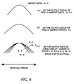
- Exemplary output waveforms of the parabolic waveform generating apparatus of the present invention are shown in FIG. 4.
- FIG. 4(a) and (b) when the data of the parabolic waveforms corresponding to the aspect ratio (16:9) and (4:3) are stored in ROM 11 and ROM 12 respectively and an aspect ratio H/V is applied to the input of the logic circuit 13, the coefficients a and (1-a) are calculated according to the equation (1).
- the two data which designate the amplitudes of the two parabolic waveforms stored in ROM 11 and ROM 12 are read out by the clock signal at each sampling time of one vertical period of the video signal, then these data values are combined according to equation (2) at each sampling time in the logic circuit 13.
- a parabolic waveform corresponding to an arbitrary aspect ratio for example, (5:3) or (4.5:3), is obtained at the output of the parabolic waveform generating circuit 6 as shown in FIG. 4(c).
- any number of parabolic waveforms corresponding to an arbitrary aspect ratio can be generated with only two ROM's.
Landscapes
- Engineering & Computer Science (AREA)
- Multimedia (AREA)
- Signal Processing (AREA)
- Details Of Television Scanning (AREA)
Applications Claiming Priority (2)
| Application Number | Priority Date | Filing Date | Title |
|---|---|---|---|
| JP4047823A JPH05219399A (ja) | 1992-02-03 | 1992-02-03 | パラボラ波形発生回路 |
| JP47823/92 | 1992-02-03 |
Publications (3)
| Publication Number | Publication Date |
|---|---|
| EP0554836A2 true EP0554836A2 (de) | 1993-08-11 |
| EP0554836A3 EP0554836A3 (en) | 1993-09-01 |
| EP0554836B1 EP0554836B1 (de) | 1997-08-20 |
Family
ID=12786077
Family Applications (1)
| Application Number | Title | Priority Date | Filing Date |
|---|---|---|---|
| EP93101581A Expired - Lifetime EP0554836B1 (de) | 1992-02-03 | 1993-02-02 | Vorrichtung zur Erzeugung von parabolischen Wellenformen |
Country Status (4)
| Country | Link |
|---|---|
| US (1) | US5301025A (de) |
| EP (1) | EP0554836B1 (de) |
| JP (1) | JPH05219399A (de) |
| DE (1) | DE69313155T2 (de) |
Cited By (6)
| Publication number | Priority date | Publication date | Assignee | Title |
|---|---|---|---|---|
| WO1996034489A1 (en) * | 1995-04-24 | 1996-10-31 | Rca Thomson Licensing Corporation | Deflection circuits for wide screen displays |
| WO1996036169A3 (en) * | 1995-05-10 | 1997-01-09 | Philips Electronics Nv | Non-linear aspect ratio adaptation |
| EP0765089A3 (de) * | 1995-09-22 | 1997-05-28 | Toshiba Kk | Digitale Konvergenzvorrichtung |
| GB2327583A (en) * | 1997-06-30 | 1999-01-27 | Daewoo Electronics Co Ltd | Parameter setting method for a multimode monitor |
| WO2001047246A1 (en) * | 1999-12-21 | 2001-06-28 | Thomson Licensing S.A. | Display correction waveform generator for multiple scanning frequencies |
| EP1089557A3 (de) * | 1999-09-30 | 2001-07-04 | Deutsche Thomson-Brandt Gmbh | Korrektions-Wellenformgenerator für eine Anzeigevorrichtung mit Mehrfrequenzabtastung |
Families Citing this family (7)
| Publication number | Priority date | Publication date | Assignee | Title |
|---|---|---|---|---|
| GB2269955B (en) * | 1992-08-07 | 1996-02-14 | British Broadcasting Corp | Method of showing 16:9 pictures on 4:3 displays |
| JP2677183B2 (ja) * | 1993-12-10 | 1997-11-17 | 日本電気株式会社 | 撮像表示システム及びその撮像カメラと表示装置 |
| JPH07250256A (ja) * | 1994-03-08 | 1995-09-26 | Sony Corp | 映像機器及び映像非線形処理回路 |
| JP3520551B2 (ja) * | 1994-03-22 | 2004-04-19 | ソニー株式会社 | 電子機器及び映像表示装置 |
| JPH1146309A (ja) * | 1997-07-28 | 1999-02-16 | Mitsubishi Electric Corp | Crtフォーカスの補正方法、crtフォーカス補正回路及びディスプレイ装置 |
| US6621870B1 (en) * | 1999-04-15 | 2003-09-16 | Diva Systems Corporation | Method and apparatus for compressing video sequences |
| US20100123822A1 (en) * | 2008-11-14 | 2010-05-20 | General Instrument Corporation | Method for Converting Between Display Information Scales |
Family Cites Families (16)
| Publication number | Priority date | Publication date | Assignee | Title |
|---|---|---|---|---|
| US3757161A (en) * | 1970-09-03 | 1973-09-04 | Commercials Electronis Inc | Television camera geometric distortion correction system |
| US4551754A (en) * | 1982-02-18 | 1985-11-05 | Rca Corporation | Compatible wide-screen color television system |
| JPS58204675A (ja) * | 1982-05-24 | 1983-11-29 | Sony Corp | 偏向ひずみ補正回路 |
| JPH0771195B2 (ja) * | 1987-05-18 | 1995-07-31 | 株式会社日立製作所 | 偏向歪補正回路 |
| DE3722172A1 (de) * | 1987-07-04 | 1989-01-12 | Thomson Brandt Gmbh | Verfahren und vorrichtung zur ausschnittvergroesserung eines fernsehbildes |
| JPH01282974A (ja) * | 1988-05-09 | 1989-11-14 | Mitsubishi Electric Corp | 上下糸巻き歪み補正回路 |
| JPH0282884A (ja) * | 1988-09-20 | 1990-03-23 | Fujitsu General Ltd | 高画質テレビジョン |
| JP2907868B2 (ja) * | 1989-05-29 | 1999-06-21 | 株式会社日立製作所 | 水平偏向歪自動補正式デイスプレイ |
| DE3927677A1 (de) * | 1989-08-23 | 1991-02-28 | Thomson Brandt Gmbh | Schaltung zur rasterkorrektur in einem fernsehgeraet |
| DE3933950A1 (de) * | 1989-10-11 | 1991-04-18 | Thomson Brandt Gmbh | Einrichtung zur rasterkorrektur in einem fernsehgeraet |
| JPH03179893A (ja) * | 1989-12-08 | 1991-08-05 | Matsushita Electric Ind Co Ltd | デジタルコンバーゼンス装置 |
| JPH03198584A (ja) * | 1989-12-27 | 1991-08-29 | Anritsu Corp | Crtの水平偏向回路 |
| JPH043663A (ja) * | 1990-04-20 | 1992-01-08 | Fujitsu General Ltd | 偏向ひずみ補正回路 |
| JPH07118778B2 (ja) * | 1990-08-20 | 1995-12-18 | 株式会社富士通ゼネラル | ピンクッション波形整形回路 |
| JPH04216274A (ja) * | 1990-12-17 | 1992-08-06 | Matsushita Electric Ind Co Ltd | テレビジョン受像機 |
| JP3327398B2 (ja) * | 1991-03-12 | 2002-09-24 | ソニー株式会社 | 偏向補正波形発生回路 |
-
1992
- 1992-02-03 JP JP4047823A patent/JPH05219399A/ja active Pending
-
1993
- 1993-01-27 US US08/009,894 patent/US5301025A/en not_active Expired - Fee Related
- 1993-02-02 EP EP93101581A patent/EP0554836B1/de not_active Expired - Lifetime
- 1993-02-02 DE DE69313155T patent/DE69313155T2/de not_active Expired - Fee Related
Cited By (15)
| Publication number | Priority date | Publication date | Assignee | Title |
|---|---|---|---|---|
| GB2314494B (en) * | 1995-04-24 | 1999-09-01 | Rca Thomson Licensing Corp | Deflection circuits for wide screen displays |
| CN1108692C (zh) * | 1995-04-24 | 2003-05-14 | Rca汤姆森许可公司 | 宽屏幕显示器的偏转电路 |
| GB2314494A (en) * | 1995-04-24 | 1997-12-24 | Rca Thomson Licensing Corp | Deflection circuits for wide screen displays |
| US5978040A (en) * | 1995-04-24 | 1999-11-02 | Rca Thomson Licensing Corporation | Deflection circuits for wide screen displays |
| WO1996034489A1 (en) * | 1995-04-24 | 1996-10-31 | Rca Thomson Licensing Corporation | Deflection circuits for wide screen displays |
| WO1996036169A3 (en) * | 1995-05-10 | 1997-01-09 | Philips Electronics Nv | Non-linear aspect ratio adaptation |
| US5835029A (en) * | 1995-09-22 | 1998-11-10 | Kabushiki Kaisha Toshiba | Digital convergence apparatus |
| EP0765089A3 (de) * | 1995-09-22 | 1997-05-28 | Toshiba Kk | Digitale Konvergenzvorrichtung |
| GB2327583A (en) * | 1997-06-30 | 1999-01-27 | Daewoo Electronics Co Ltd | Parameter setting method for a multimode monitor |
| EP1089556A3 (de) * | 1999-09-30 | 2001-08-01 | Thomson Licensing S.A. | Korrektions-Wellenformgenerator für eine Anzeigevorrichtung mit Mehrfrequenzabtastung |
| EP1089557A3 (de) * | 1999-09-30 | 2001-07-04 | Deutsche Thomson-Brandt Gmbh | Korrektions-Wellenformgenerator für eine Anzeigevorrichtung mit Mehrfrequenzabtastung |
| US6351086B1 (en) | 1999-09-30 | 2002-02-26 | Thomson Lincensing S. A. | Display correction waveform generator for multiple scanning |
| WO2001047246A1 (en) * | 1999-12-21 | 2001-06-28 | Thomson Licensing S.A. | Display correction waveform generator for multiple scanning frequencies |
| US6774585B2 (en) | 1999-12-21 | 2004-08-10 | Thomson Licensing S.A. | Display correction waveform generator for multiple scanning frequencies |
| CN1310496C (zh) * | 1999-12-21 | 2007-04-11 | 汤姆森特许公司 | 用于多扫描频率的显示校正波形发生器 |
Also Published As
| Publication number | Publication date |
|---|---|
| JPH05219399A (ja) | 1993-08-27 |
| DE69313155T2 (de) | 1997-12-18 |
| EP0554836A3 (en) | 1993-09-01 |
| DE69313155D1 (de) | 1997-09-25 |
| EP0554836B1 (de) | 1997-08-20 |
| US5301025A (en) | 1994-04-05 |
Similar Documents
| Publication | Publication Date | Title |
|---|---|---|
| EP0663768B1 (de) | Verfahren und digitale Schaltung zum Aufheben des Zeilensprungverfahrens während der Darstellung von Videobildern | |
| EP0685829B1 (de) | Verfahren zum senkrechten Filtern bei rasterabgetasteten Anzeigevorrichtungen | |
| US6717622B2 (en) | System and method for scalable resolution enhancement of a video image | |
| US5301025A (en) | Parabolic waveform generating apparatus | |
| EP0194066B1 (de) | Videosignalverarbeitung | |
| KR100416370B1 (ko) | 비디오필드들을순차주사비디오프레임들로디인터레이싱하기위한방법및장치 | |
| KR100342964B1 (ko) | 감마 보정 회로 및 감마 보정 방법 | |
| EP0488542A1 (de) | Schaltung zur Verbesserung der Bildqualität | |
| US5666165A (en) | Video signal compression apparatus for horizontal compression of a video signal | |
| RU2118064C1 (ru) | Способ и устройство для обработки видеокадра | |
| EP0461996A2 (de) | Bildverarbeitungsgerät | |
| US5459525A (en) | Video signal converting device and noise eliminator used therein | |
| WO1997041680A2 (en) | Spline waveform generation | |
| US4620228A (en) | Television signal generator | |
| GB2224410A (en) | Video image magnification system | |
| KR100319878B1 (ko) | 비선형특성보정장치및방법 | |
| JP2552742B2 (ja) | 適応型輪郭補正回路 | |
| KR100922244B1 (ko) | 신호 처리 장치 및 화상 출력 장치 | |
| US5903316A (en) | Information signal processing apparatus | |
| RU2022336C1 (ru) | Устройство для формирования видеосигнала | |
| CN1432979A (zh) | 通过成形统计滤波实现的图像假频抑制 | |
| KR960012484B1 (ko) | 종횡비 변환 출력장치 | |
| EP0970582A1 (de) | Bilinearer dezimator mit fehlerkompensation | |
| KR0174457B1 (ko) | 브이오디용 그래픽 처리방법 | |
| KR100297601B1 (ko) | 고품위디지탈영상을구현하는화질보상회로및그방법 |
Legal Events
| Date | Code | Title | Description |
|---|---|---|---|
| PUAI | Public reference made under article 153(3) epc to a published international application that has entered the european phase |
Free format text: ORIGINAL CODE: 0009012 |
|
| PUAL | Search report despatched |
Free format text: ORIGINAL CODE: 0009013 |
|
| AK | Designated contracting states |
Kind code of ref document: A2 Designated state(s): DE FR GB |
|
| AK | Designated contracting states |
Kind code of ref document: A3 Designated state(s): DE FR GB |
|
| 17P | Request for examination filed |
Effective date: 19931015 |
|
| 17Q | First examination report despatched |
Effective date: 19940215 |
|
| GRAG | Despatch of communication of intention to grant |
Free format text: ORIGINAL CODE: EPIDOS AGRA |
|
| GRAH | Despatch of communication of intention to grant a patent |
Free format text: ORIGINAL CODE: EPIDOS IGRA |
|
| GRAH | Despatch of communication of intention to grant a patent |
Free format text: ORIGINAL CODE: EPIDOS IGRA |
|
| GRAA | (expected) grant |
Free format text: ORIGINAL CODE: 0009210 |
|
| AK | Designated contracting states |
Kind code of ref document: B1 Designated state(s): DE FR GB |
|
| REF | Corresponds to: |
Ref document number: 69313155 Country of ref document: DE Date of ref document: 19970925 |
|
| ET | Fr: translation filed | ||
| PGFP | Annual fee paid to national office [announced via postgrant information from national office to epo] |
Ref country code: GB Payment date: 19980121 Year of fee payment: 6 |
|
| PGFP | Annual fee paid to national office [announced via postgrant information from national office to epo] |
Ref country code: FR Payment date: 19980213 Year of fee payment: 6 |
|
| PGFP | Annual fee paid to national office [announced via postgrant information from national office to epo] |
Ref country code: DE Payment date: 19980331 Year of fee payment: 6 |
|
| PLBE | No opposition filed within time limit |
Free format text: ORIGINAL CODE: 0009261 |
|
| STAA | Information on the status of an ep patent application or granted ep patent |
Free format text: STATUS: NO OPPOSITION FILED WITHIN TIME LIMIT |
|
| 26N | No opposition filed | ||
| PG25 | Lapsed in a contracting state [announced via postgrant information from national office to epo] |
Ref country code: GB Free format text: LAPSE BECAUSE OF NON-PAYMENT OF DUE FEES Effective date: 19990202 |
|
| GBPC | Gb: european patent ceased through non-payment of renewal fee |
Effective date: 19990202 |
|
| PG25 | Lapsed in a contracting state [announced via postgrant information from national office to epo] |
Ref country code: FR Free format text: LAPSE BECAUSE OF NON-PAYMENT OF DUE FEES Effective date: 19991029 |
|
| PG25 | Lapsed in a contracting state [announced via postgrant information from national office to epo] |
Ref country code: DE Free format text: LAPSE BECAUSE OF NON-PAYMENT OF DUE FEES Effective date: 19991201 |
|
| REG | Reference to a national code |
Ref country code: FR Ref legal event code: ST |