EP0558075A2 - Dispositif semi-conducteur en couche mince de polysilicum - Google Patents
Dispositif semi-conducteur en couche mince de polysilicum Download PDFInfo
- Publication number
- EP0558075A2 EP0558075A2 EP93103140A EP93103140A EP0558075A2 EP 0558075 A2 EP0558075 A2 EP 0558075A2 EP 93103140 A EP93103140 A EP 93103140A EP 93103140 A EP93103140 A EP 93103140A EP 0558075 A2 EP0558075 A2 EP 0558075A2
- Authority
- EP
- European Patent Office
- Prior art keywords
- thin film
- size
- polysilicon thin
- semiconductor device
- field effect
- Prior art date
- Legal status (The legal status is an assumption and is not a legal conclusion. Google has not performed a legal analysis and makes no representation as to the accuracy of the status listed.)
- Granted
Links
Images


Classifications
-
- H—ELECTRICITY
- H10—SEMICONDUCTOR DEVICES; ELECTRIC SOLID-STATE DEVICES NOT OTHERWISE PROVIDED FOR
- H10P—GENERIC PROCESSES OR APPARATUS FOR THE MANUFACTURE OR TREATMENT OF DEVICES COVERED BY CLASS H10
- H10P14/00—Formation of materials, e.g. in the shape of layers or pillars
- H10P14/20—Formation of materials, e.g. in the shape of layers or pillars of semiconductor materials
- H10P14/38—Formation of materials, e.g. in the shape of layers or pillars of semiconductor materials characterised by treatments done after the formation of the materials
- H10P14/3802—Crystallisation or recrystallisation of non-monocrystalline semiconductor materials, e.g. regrowth
- H10P14/3808—Crystallisation or recrystallisation of non-monocrystalline semiconductor materials, e.g. regrowth using laser beams
- H10P14/3816—Pulsed laser beam
-
- H—ELECTRICITY
- H10—SEMICONDUCTOR DEVICES; ELECTRIC SOLID-STATE DEVICES NOT OTHERWISE PROVIDED FOR
- H10D—INORGANIC ELECTRIC SEMICONDUCTOR DEVICES
- H10D30/00—Field-effect transistors [FET]
- H10D30/01—Manufacture or treatment
- H10D30/021—Manufacture or treatment of FETs having insulated gates [IGFET]
- H10D30/031—Manufacture or treatment of FETs having insulated gates [IGFET] of thin-film transistors [TFT]
- H10D30/0312—Manufacture or treatment of FETs having insulated gates [IGFET] of thin-film transistors [TFT] characterised by the gate electrodes
- H10D30/0314—Manufacture or treatment of FETs having insulated gates [IGFET] of thin-film transistors [TFT] characterised by the gate electrodes of lateral top-gate TFTs comprising only a single gate
-
- H—ELECTRICITY
- H10—SEMICONDUCTOR DEVICES; ELECTRIC SOLID-STATE DEVICES NOT OTHERWISE PROVIDED FOR
- H10D—INORGANIC ELECTRIC SEMICONDUCTOR DEVICES
- H10D30/00—Field-effect transistors [FET]
- H10D30/01—Manufacture or treatment
- H10D30/021—Manufacture or treatment of FETs having insulated gates [IGFET]
- H10D30/031—Manufacture or treatment of FETs having insulated gates [IGFET] of thin-film transistors [TFT]
- H10D30/0321—Manufacture or treatment of FETs having insulated gates [IGFET] of thin-film transistors [TFT] comprising silicon, e.g. amorphous silicon or polysilicon
-
- H—ELECTRICITY
- H10—SEMICONDUCTOR DEVICES; ELECTRIC SOLID-STATE DEVICES NOT OTHERWISE PROVIDED FOR
- H10D—INORGANIC ELECTRIC SEMICONDUCTOR DEVICES
- H10D30/00—Field-effect transistors [FET]
- H10D30/60—Insulated-gate field-effect transistors [IGFET]
- H10D30/67—Thin-film transistors [TFT]
- H10D30/6729—Thin-film transistors [TFT] characterised by the electrodes
- H10D30/673—Thin-film transistors [TFT] characterised by the electrodes characterised by the shapes, relative sizes or dispositions of the gate electrodes
- H10D30/6731—Top-gate only TFTs
-
- H—ELECTRICITY
- H10—SEMICONDUCTOR DEVICES; ELECTRIC SOLID-STATE DEVICES NOT OTHERWISE PROVIDED FOR
- H10D—INORGANIC ELECTRIC SEMICONDUCTOR DEVICES
- H10D30/00—Field-effect transistors [FET]
- H10D30/60—Insulated-gate field-effect transistors [IGFET]
- H10D30/67—Thin-film transistors [TFT]
- H10D30/674—Thin-film transistors [TFT] characterised by the active materials
- H10D30/6741—Group IV materials, e.g. germanium or silicon carbide
- H10D30/6743—Silicon
- H10D30/6745—Polycrystalline or microcrystalline silicon
-
- H—ELECTRICITY
- H10—SEMICONDUCTOR DEVICES; ELECTRIC SOLID-STATE DEVICES NOT OTHERWISE PROVIDED FOR
- H10P—GENERIC PROCESSES OR APPARATUS FOR THE MANUFACTURE OR TREATMENT OF DEVICES COVERED BY CLASS H10
- H10P14/00—Formation of materials, e.g. in the shape of layers or pillars
- H10P14/20—Formation of materials, e.g. in the shape of layers or pillars of semiconductor materials
- H10P14/29—Formation of materials, e.g. in the shape of layers or pillars of semiconductor materials characterised by the substrates
- H10P14/2901—Materials
- H10P14/2921—Materials being crystalline insulating materials
-
- H—ELECTRICITY
- H10—SEMICONDUCTOR DEVICES; ELECTRIC SOLID-STATE DEVICES NOT OTHERWISE PROVIDED FOR
- H10P—GENERIC PROCESSES OR APPARATUS FOR THE MANUFACTURE OR TREATMENT OF DEVICES COVERED BY CLASS H10
- H10P14/00—Formation of materials, e.g. in the shape of layers or pillars
- H10P14/20—Formation of materials, e.g. in the shape of layers or pillars of semiconductor materials
- H10P14/34—Deposited materials, e.g. layers
- H10P14/3402—Deposited materials, e.g. layers characterised by the chemical composition
- H10P14/3404—Deposited materials, e.g. layers characterised by the chemical composition being Group IVA materials
- H10P14/3411—Silicon, silicon germanium or germanium
-
- H—ELECTRICITY
- H10—SEMICONDUCTOR DEVICES; ELECTRIC SOLID-STATE DEVICES NOT OTHERWISE PROVIDED FOR
- H10P—GENERIC PROCESSES OR APPARATUS FOR THE MANUFACTURE OR TREATMENT OF DEVICES COVERED BY CLASS H10
- H10P14/00—Formation of materials, e.g. in the shape of layers or pillars
- H10P14/20—Formation of materials, e.g. in the shape of layers or pillars of semiconductor materials
- H10P14/34—Deposited materials, e.g. layers
- H10P14/3451—Structure
- H10P14/3452—Microstructure
- H10P14/3456—Polycrystalline
-
- H—ELECTRICITY
- H10—SEMICONDUCTOR DEVICES; ELECTRIC SOLID-STATE DEVICES NOT OTHERWISE PROVIDED FOR
- H10P—GENERIC PROCESSES OR APPARATUS FOR THE MANUFACTURE OR TREATMENT OF DEVICES COVERED BY CLASS H10
- H10P14/00—Formation of materials, e.g. in the shape of layers or pillars
- H10P14/20—Formation of materials, e.g. in the shape of layers or pillars of semiconductor materials
- H10P14/34—Deposited materials, e.g. layers
- H10P14/3466—Crystal orientation
Definitions
- the present invention relates to a semiconductor device, such as a thin-film transistor, having in its main part a polysilicon thin film for transferring carriers.
- a technique of forming a thin-film transistor on an insulating substrate is known in a field of active matrix liquid crystal displays (LCDs).
- the technique allows a semiconductor integrated circuit to be formed on a transparent insulating substrate formed of, for example, glass, or a large insulating substrate which cannot be formed of a monocrystalline semiconductor.
- a thin-film transistor generally includes an active layer made of amorphous silicon or polysilicon. Since amorphous silicon can be formed at a low temperature, it is applicable to an active matrix LCD which must be formed on a glass substrate having a low melting point.
- amorphous silicon has a low electron mobility, it has been used only as a switching element for charging a pixel capacitor electrode to apply an electric field to a liquid crystal.
- An active layer made of polysilicon must be used in a circuit element, e.g., a driver circuit, a ROM, a RAM or a CPU, which must be driven at a high speed.
- a driver circuit of a high-quality, large-screen liquid crystal TV or a high-definition office automation (OA) liquid crystal display panel is driven at a clock frequency of about 10 MHz.
- OA office automation
- a field effect mobility ⁇ FE of 50 cm2/V ⁇ sec or more, preferably 80 cm2/V ⁇ sec or more is required.
- the field effect mobility ⁇ FE of a polysilicon thin-film transistor known to the public at present is at most 30 cm2/V ⁇ sec.
- the semiconductor device of the present invention has a polysilicon thin film in its main part, wherein a grain size is substantially the same as a crystallite size on the (111) plane and the crystallite size is greater than a thickness of the polysilicon thin film (EPC: 180 nm or greater).
- the field effect mobility ⁇ FE of a polysilicon thin-film transistor is determined by grain sizes of silicon crystals constituting an active layer, i.e. a polysilicon thin film.
- a polysilicon thin film there is another determinant such as a trap of carriers which may be caused depending on the state of an interface between the polysilicon thin film and a gate insulating film, it has been considered important to form large and uniform grains, as far as the crystal structure is concerned.
- techniques for an enhancement of the electron mobility by increasing the size and the uniformness of grains have been studied.
- the present inventor discovered throughout his researches that it is difficult to enhance the electron mobility only by increasing the grain size of a polysilicon thin film. According to the inventor's research, the electron mobility was not increased beyond a predetermined value however the grain size is increased, whereas it was satisfactorily increased even when the grain size was not very large.
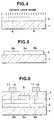
- Figs. 1 to 6 show steps of manufacturing a thin-film transistor according to an embodiment of the present invention.
- the structure of the thin-film transistor and a method of manufacturing the same will now be described with reference to these drawings in sequence.
- an amorphous silicon thin film 2 is deposited on the upper surface of an insulating substrate 1 made of quartz or the like by an LP-CVD (Low Pressure Chemical Vapor Deposition) method at a temperature of 550°C. Thereafter, as shown in Fig. 2, XeCl excimer laser beams are applied to the substrate, thereby polycrystallizing the amorphous silicon thin film 2 into a polysilicon thin film 3 by a liquid-phase growth. The crystal structure of the polysilicon thin film 3 in this state will be described later. Then, as shown in Fig.
- LP-CVD Low Pressure Chemical Vapor Deposition
- a photoresist film 5 is formed on the upper surface of the polysilicon thin film 3, and patterned not to leave on the regions of film 3 which correspond to source and drain forming regions 4.
- impurities such as phosphorus ions or boron ions are injected to a high concentration into the source and drain forming regions 4 of the polysilicon thin film 3, thereby forming impurity-injected regions 6.
- the photoresist film 5 is removed.
- XeCl excimer laser beams are applied to the polysilicon thin film 3 again to activate the impurities injected in the regions 6. Then, as shown in Fig.
- a central portion of the polysilicon thin film 3 serves as a channel region 3a, and side portions thereof as source and drain regions 3b formed of activated impurity regions.
- a gate-insulating film 7 formed of a silicon oxide film and the like is formed on the upper surface of the assembly.
- a gate electrode 8 made of chrome and the like is formed on the upper surface of a portion of the gate insulating film 7 which corresponds to the channel region 3a, by means of a depositing and a patterning.
- a passivating insulating film 9 made of silicon nitride or the like is formed on the entire upper surface of the assembly.
- contact holes 10 are formed in those portions of the passivating insulating film 9 and the gate-insulating film 7 which correspond to the source and drain regions 3b.
- source and drain electrodes 11 made of aluminum and the like are patterned on the passivating insulating film 9 and connected to the source and drain regions 3b through the contact holes 10 are formed on the passivating insulating film 9 and in the holes 10.
- a polysilicon thin film according to an embodiment of the present invention was prepared in the following manner: an amorphous silicon thin film having a thickness of about 500 ⁇ was deposited on the upper surface of a quartz substrate, and XeCl excimer laser beams were applied twice to the amorphous silicon thin film at a temperature of about 250°C under an energy density of about 300 mJ/cm2, so that the amorphous silicon thin film was poly-crystallized in a liquid-phase growth, to obtain a polysilicon thin film.
- a polysilicon thin film according to conventional art was prepared in the following manner: an amorphous silicon thin film having a thickness of about 500 ⁇ was deposited on the upper surface of a quartz substrate; the substrate was heated in a nitrogen atmosphere at a temperature of about 600°C for 48 hours, so that the amorphous silicon thin film was polycrystallized in a solid-phase growth, to obtain a polysilicon thin film.
- the crystal structures were analyzed by using a (Transmission Electron Microscope) and an XD (X-ray Diffractor analysis).
- grain size was measured with JEM-2010 of JEOL (acceleration voltage: 200 kV, magnification: 5 ⁇ 105 to 1.5 ⁇ 106).
- the grain size of the embodiment was 246 nm, whereas the grain size of the prior art was 1.2 ⁇ m, which is 5 times greater than the grain size of the embodiment.
- Each grain size C ⁇ indicated in Table 1 is an average calculated based on the measured values at 30 points.
- RU-200 of Rigaku Denki Company (radiation source: CuKa, maximum output: 12 kW) was used for the measurement.
- step scanning for 2 seconds was performed three times (30 minutes in total) with a rotational angle of 0.01° within a range of ⁇ 1.5° on each of the peak planes, i.e., the (111) plane, the (220) plane, and the (311) plane, under the condition of the incident X-ray intensity 50 kV and the current of 180 mA.
- the crystallite size was calculated from the peak width at half height by use of the following equation of Scherrer.
- D hk1 ⁇ /(B ⁇ cos ⁇ B) where Dhk1 denotes a crystallite size in a direction perpendicular to the (hk1) plane; ⁇ , a wavelength of an X-ray beam; B, a half width; and ⁇ B, a Bragg's angle.
- Table 1 The results of the measurement are shown in Table 1.
- the average values of the crystallite size measured in the three-time measurement were 37 nm on the (111) plane, 23 nm on the (220) plane, and 36 nm on the (311) plane, whereas in the present embodiment, the average values were much greater than in the conventional device, i.e., 202 nm on the (111) plane, 144 nm on the (220) plane, and 103 nm on the (311) plane.
- Coplanar type field effect thin-film transistors as shown in Fig. 6 were manufactured using the thin films of the embodiment and the conventional art, and the field effect mobilities ⁇ FE thereof were measured. As shown in Table 1, the mobility in the conventional thin-film transistor was 30 cm2/V ⁇ sec, whereas the mobility in the thin-film transistor of the present embodiment was 90 cm2/V ⁇ sec, which is three times greater than that of the conventional transistor. The measurement result represents that the field effect mobility ⁇ FE is correlated to the crystallite size rather than the grain size.
- Figs. 9A, 9B, and 10 show results of the measurement.
- the sample indicated in Table 1 includes an amorphous silicon film deposited on the substrate to a thickness of 500 ⁇ by a LPCVD method
- some of the samples indicated in Figs. 9A, 9B, and 10 are formed by a plasma CVD method or have various thicknesses (500 to 3000 ⁇ ).
- Fig. 9A shows the relationship between grain size C ⁇ and field effect mobility ⁇ FE
- Fig. 9B shows the relationship between crystallite size and field effect mobility ⁇ FE on the (111) plane.
- Fig. 9A shows the relationship between grain size C ⁇ and field effect mobility ⁇ FE
- Fig. 9B shows the relationship between crystallite size and field effect mobility ⁇ FE on the (111) plane.
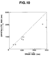
- FIG. 10 shows the relationship between a grain size and a crystallite size on the (111) plane.
- a crystal size measured by a low-angle incidence method must be corrected, the values of the crystallite size indicated in Figs. 9B and 10 are calculated by the equation of Scherrer and uncorrected.
- Fig. 9A there is a specific correlation between the grain size C ⁇ and the field effect mobility ⁇ FE .
- Fig. 9B there is a specific correlation between the crystallite size on the (111) plane and the field effect mobility ⁇ FE .
- Conditions for the correlations can be understood from Fig. 10.
- crystallite size approximates to grain size. In the range that the grain size is 100 nm or smaller, it is substantially the same as the crystallite size. In the range that the grain size is greater than 100 nm, the ratio of the crystallite size to the grain size is slightly smaller than 1. In case that grain size is about 300 nm, the crystallite size is about 60 to 70 % of the grain size. If a thin film having the crystallite size the same as grain size in the range of 200 to 300 nm or greater of the grain size by improving the manufacturing method is obtained, the field effect mobility ⁇ FE can be further increased.
- the crystallite sizes on the (111), (220), and (311) planes of the embodiment are respectively 202 nm, 144 nm, and 103 nm, which are all greater than the thickness of the polysilicon thin film, i.e., 500 ⁇ .
- the crystallite size on the (111) plane i.e. the maximum peak plane, is 37 nm which is smaller than the thickness of the polysilicon thin film, 500 ⁇ .
- the field effect mobility ⁇ FE can be more greatly increased than in the conventional device, if the crystallite size of the polysilicon thin film is greater than the thickness of the polysilicon thin film.
- the thickness of the polysilicon thin film is 500 to 3000 ⁇ , the field effect mobility ⁇ FE of at least 50 cm2/V ⁇ sec is ensured.
- the present invention is not limited to a field effect thin-film transistor, but is applicable to any type of semiconductor device having a polysilicon thin film as its main part to transfer carriers.
- a driver circuit which is operated with a clock frequency of about 10 MHz can be formed using a semiconductor device. Note that when the crystallite size is 60 to 70 % or greater of the grain size, these sizes are considered to be "substantially the same”.
Landscapes
- Thin Film Transistor (AREA)
- Recrystallisation Techniques (AREA)
Applications Claiming Priority (3)
| Application Number | Priority Date | Filing Date | Title |
|---|---|---|---|
| JP4075921A JP2935446B2 (ja) | 1992-02-28 | 1992-02-28 | 半導体装置 |
| JP75921/92 | 1992-02-28 | ||
| JP7592192 | 1992-02-28 |
Publications (3)
| Publication Number | Publication Date |
|---|---|
| EP0558075A2 true EP0558075A2 (fr) | 1993-09-01 |
| EP0558075A3 EP0558075A3 (fr) | 1994-01-19 |
| EP0558075B1 EP0558075B1 (fr) | 2004-08-18 |
Family
ID=13590260
Family Applications (1)
| Application Number | Title | Priority Date | Filing Date |
|---|---|---|---|
| EP93103140A Expired - Lifetime EP0558075B1 (fr) | 1992-02-28 | 1993-02-26 | Méthode pour la fabrication d'un transistor en couche mince de polysilicium |
Country Status (9)
| Country | Link |
|---|---|
| US (1) | US5949091A (fr) |
| EP (1) | EP0558075B1 (fr) |
| JP (1) | JP2935446B2 (fr) |
| KR (1) | KR970004844B1 (fr) |
| CN (1) | CN1026041C (fr) |
| CA (1) | CA2090096C (fr) |
| DE (1) | DE69333592T2 (fr) |
| SG (1) | SG55060A1 (fr) |
| TW (1) | TW335216U (fr) |
Cited By (1)
| Publication number | Priority date | Publication date | Assignee | Title |
|---|---|---|---|---|
| US6670638B2 (en) * | 2000-09-25 | 2003-12-30 | Hitachi, Ltd. | Liquid crystal display element and method of manufacturing the same |
Families Citing this family (9)
| Publication number | Priority date | Publication date | Assignee | Title |
|---|---|---|---|---|
| TW264575B (fr) * | 1993-10-29 | 1995-12-01 | Handotai Energy Kenkyusho Kk | |
| US6059873A (en) | 1994-05-30 | 2000-05-09 | Semiconductor Energy Laboratory Co., Ltd. | Optical processing method with control of the illumination energy of laser light |
| US6100119A (en) * | 1995-08-31 | 2000-08-08 | Lg Electronics Inc. | Thin film transistor and method for fabricating the same |
| JPH11145056A (ja) * | 1997-11-07 | 1999-05-28 | Sony Corp | 半導体材料 |
| JP2000208771A (ja) * | 1999-01-11 | 2000-07-28 | Hitachi Ltd | 半導体装置、液晶表示装置およびこれらの製造方法 |
| JP4437570B2 (ja) * | 1999-07-12 | 2010-03-24 | 株式会社ルネサステクノロジ | 半導体装置及び半導体装置の製造方法 |
| US6229611B1 (en) * | 1999-09-20 | 2001-05-08 | United Microelectronics Corp. | Method of detecting a transparent quartz wafer in a semiconductor equipment |
| JP6941473B2 (ja) * | 2017-04-26 | 2021-09-29 | 株式会社日本製鋼所 | ディスプレイの製造方法、ディスプレイ及び液晶テレビ |
| US11024736B2 (en) * | 2019-08-09 | 2021-06-01 | Micron Technology, Inc. | Transistor and methods of forming integrated circuitry |
Family Cites Families (12)
| Publication number | Priority date | Publication date | Assignee | Title |
|---|---|---|---|---|
| JPS57194517A (en) * | 1981-05-27 | 1982-11-30 | Toshiba Corp | Manufacture of semiconductor crystal film |
| JPH0620122B2 (ja) * | 1982-01-19 | 1994-03-16 | キヤノン株式会社 | 半導体素子 |
| US4649624A (en) * | 1983-10-03 | 1987-03-17 | The United States Of America As Represented By The Secretary Of The Navy | Fabrication of semiconductor devices in recrystallized semiconductor films on electrooptic substrates |
| CA1239706A (fr) * | 1984-11-26 | 1988-07-26 | Hisao Hayashi | Faconnage d'une pellicule semiconductrice en couche mince |
| JPS63292618A (ja) * | 1987-05-26 | 1988-11-29 | Nec Corp | Soi基板の製造方法 |
| JP2880175B2 (ja) * | 1988-11-30 | 1999-04-05 | 株式会社日立製作所 | レーザアニール方法及び薄膜半導体装置 |
| US5200630A (en) * | 1989-04-13 | 1993-04-06 | Sanyo Electric Co., Ltd. | Semiconductor device |
| JP2655924B2 (ja) * | 1990-02-19 | 1997-09-24 | キヤノン株式会社 | 多結晶半導体薄膜形成方法 |
| JP2973492B2 (ja) * | 1990-08-22 | 1999-11-08 | ソニー株式会社 | 半導体薄膜の結晶化方法 |
| EP0499979A3 (en) * | 1991-02-16 | 1993-06-09 | Semiconductor Energy Laboratory Co., Ltd. | Electro-optical device |
| JPH04267517A (ja) * | 1991-02-22 | 1992-09-24 | Toshiba Corp | 半導体薄膜の形成方法 |
| JPH04311038A (ja) * | 1991-04-09 | 1992-11-02 | Toshiba Corp | 薄膜トランジスタの製造方法 |
-
1992
- 1992-02-28 JP JP4075921A patent/JP2935446B2/ja not_active Expired - Lifetime
-
1993
- 1993-02-20 KR KR1019930002385A patent/KR970004844B1/ko not_active Expired - Lifetime
- 1993-02-22 CA CA002090096A patent/CA2090096C/fr not_active Expired - Lifetime
- 1993-02-23 US US08/021,333 patent/US5949091A/en not_active Expired - Lifetime
- 1993-02-25 TW TW084217964U patent/TW335216U/zh unknown
- 1993-02-26 CN CN93101559A patent/CN1026041C/zh not_active Expired - Lifetime
- 1993-02-26 EP EP93103140A patent/EP0558075B1/fr not_active Expired - Lifetime
- 1993-02-26 SG SG1996004011A patent/SG55060A1/en unknown
- 1993-02-26 DE DE69333592T patent/DE69333592T2/de not_active Expired - Lifetime
Cited By (1)
| Publication number | Priority date | Publication date | Assignee | Title |
|---|---|---|---|---|
| US6670638B2 (en) * | 2000-09-25 | 2003-12-30 | Hitachi, Ltd. | Liquid crystal display element and method of manufacturing the same |
Also Published As
| Publication number | Publication date |
|---|---|
| SG55060A1 (en) | 1998-12-21 |
| EP0558075A3 (fr) | 1994-01-19 |
| CN1026041C (zh) | 1994-09-28 |
| CA2090096C (fr) | 1998-08-11 |
| KR970004844B1 (ko) | 1997-04-04 |
| CN1076551A (zh) | 1993-09-22 |
| US5949091A (en) | 1999-09-07 |
| DE69333592D1 (de) | 2004-09-23 |
| DE69333592T2 (de) | 2005-01-05 |
| JPH05243576A (ja) | 1993-09-21 |
| CA2090096A1 (fr) | 1993-08-29 |
| HK1013521A1 (en) | 1999-08-27 |
| JP2935446B2 (ja) | 1999-08-16 |
| EP0558075B1 (fr) | 2004-08-18 |
| KR930018754A (ko) | 1993-09-22 |
| TW335216U (en) | 1998-06-21 |
Similar Documents
| Publication | Publication Date | Title |
|---|---|---|
| EP0459763B1 (fr) | Transistors en couche mince | |
| US5864150A (en) | Hybrid polysilicon/amorphous silicon TFT and method of fabrication | |
| US6492213B1 (en) | Semiconductor device, thin film transistor and method for producing the same, and liquid crystal display apparatus and method for producing the same | |
| US5637515A (en) | Method of making thin film transistor using lateral crystallization | |
| US7238558B2 (en) | Semiconductor device and method of fabricating the same | |
| DE69522370T2 (de) | SiGe-Dünnfilm-Halbleiteranordnung mit SiGe Schichtstruktur und Verfahren zur Herstellung | |
| US6271062B1 (en) | Thin film semiconductor device including a semiconductor film with high field-effect mobility | |
| US5696386A (en) | Semiconductor device | |
| EP0523768B1 (fr) | Fabrication d'un transistor à couches minces | |
| US6338990B1 (en) | Method for fabricating thin-film transistor | |
| KR100229676B1 (ko) | 셀프얼라인 박막트랜지스터 제조방법 | |
| US5231297A (en) | Thin film transistor | |
| US20060105514A1 (en) | Thin film semiconductor device and method of manufacturing the same | |
| US5576229A (en) | Method of fabricating a thin-film transistor and liquid-crystal display apparatus | |
| US5877526A (en) | Semiconductor device having polysilicon thin-film | |
| EP0558075A2 (fr) | Dispositif semi-conducteur en couche mince de polysilicum | |
| EP0459836B1 (fr) | Procédé pour fabriquer des transistors à film mince | |
| US5733793A (en) | Process formation of a thin film transistor | |
| US5937304A (en) | Method for fabricating semiconductor device and method for producing liquid crystal display apparatus | |
| US6639245B2 (en) | Active matrix display device having high intensity and high precision and manufacturing method thereof | |
| JP3347340B2 (ja) | 薄膜トランジスタの製造方法 | |
| JPH04340725A (ja) | 薄膜トランジスタの製造方法 | |
| HK1013521B (en) | Method for fabricating a polysilicon thin film transistor | |
| JPH0888172A (ja) | 多結晶シリコン膜の作製方法 | |
| KR0138874B1 (ko) | 박막 트랜지스터의 제조방법 |
Legal Events
| Date | Code | Title | Description |
|---|---|---|---|
| PUAI | Public reference made under article 153(3) epc to a published international application that has entered the european phase |
Free format text: ORIGINAL CODE: 0009012 |
|
| 17P | Request for examination filed |
Effective date: 19930226 |
|
| AK | Designated contracting states |
Kind code of ref document: A2 Designated state(s): DE FR GB |
|
| PUAL | Search report despatched |
Free format text: ORIGINAL CODE: 0009013 |
|
| AK | Designated contracting states |
Kind code of ref document: A3 Designated state(s): DE FR GB |
|
| 17Q | First examination report despatched |
Effective date: 19960320 |
|
| APAB | Appeal dossier modified |
Free format text: ORIGINAL CODE: EPIDOS NOAPE |
|
| APAB | Appeal dossier modified |
Free format text: ORIGINAL CODE: EPIDOS NOAPE |
|
| APAD | Appeal reference recorded |
Free format text: ORIGINAL CODE: EPIDOS REFNE |
|
| APAB | Appeal dossier modified |
Free format text: ORIGINAL CODE: EPIDOS NOAPE |
|
| RAP1 | Party data changed (applicant data changed or rights of an application transferred) |
Owner name: CASIO COMPUTER CO., LTD. |
|
| RTI1 | Title (correction) |
Free format text: METHOD FOR FABRICATING A POLYSILICON THIN FILM TRANSISTOR |
|
| GRAG | Despatch of communication of intention to grant |
Free format text: ORIGINAL CODE: EPIDOS AGRA |
|
| RIC1 | Information provided on ipc code assigned before grant |
Free format text: 6H 01L 29/04 A, 6H 01L 29/16 B, 6H 01L 21/20 B, 6H 01L 29/786 B |
|
| RTI1 | Title (correction) |
Free format text: METHOD FOR FABRICATING A POLYSILICON THIN FILM TRANSISTOR |
|
| GRAG | Despatch of communication of intention to grant |
Free format text: ORIGINAL CODE: EPIDOS AGRA |
|
| APAB | Appeal dossier modified |
Free format text: ORIGINAL CODE: EPIDOS NOAPE |
|
| APAB | Appeal dossier modified |
Free format text: ORIGINAL CODE: EPIDOS NOAPE |
|
| APAD | Appeal reference recorded |
Free format text: ORIGINAL CODE: EPIDOS REFNE |
|
| APAB | Appeal dossier modified |
Free format text: ORIGINAL CODE: EPIDOS NOAPE |
|
| APBT | Appeal procedure closed |
Free format text: ORIGINAL CODE: EPIDOSNNOA9E |
|
| GRAP | Despatch of communication of intention to grant a patent |
Free format text: ORIGINAL CODE: EPIDOSNIGR1 |
|
| RIC1 | Information provided on ipc code assigned before grant |
Ipc: 7H 01L 29/786 B Ipc: 7H 01L 21/20 B Ipc: 7H 01L 29/16 B Ipc: 7H 01L 29/04 A |
|
| RTI1 | Title (correction) |
Free format text: METHOD FOR FABRICATING A POLYSILICON THIN FILM TRANSISTOR |
|
| RIC1 | Information provided on ipc code assigned before grant |
Ipc: 7H 01L 29/786 B Ipc: 7H 01L 21/20 B Ipc: 7H 01L 29/16 B Ipc: 7H 01L 29/04 A |
|
| RTI1 | Title (correction) |
Free format text: METHOD FOR FABRICATING A POLYSILICON THIN FILM TRANSISTOR |
|
| RIC1 | Information provided on ipc code assigned before grant |
Ipc: 7H 01L 29/786 B Ipc: 7H 01L 21/20 B Ipc: 7H 01L 29/16 B Ipc: 7H 01L 29/04 A |
|
| RTI1 | Title (correction) |
Free format text: METHOD FOR FABRICATING A POLYSILICON THIN FILM TRANSISTOR |
|
| RIC1 | Information provided on ipc code assigned before grant |
Ipc: 7H 01L 29/786 B Ipc: 7H 01L 21/20 B Ipc: 7H 01L 29/16 B Ipc: 7H 01L 29/04 A |
|
| RTI1 | Title (correction) |
Free format text: METHOD FOR FABRICATING A POLYSILICON THIN FILM TRANSISTOR |
|
| GRAS | Grant fee paid |
Free format text: ORIGINAL CODE: EPIDOSNIGR3 |
|
| GRAA | (expected) grant |
Free format text: ORIGINAL CODE: 0009210 |
|
| GRAU | Approval following communication of intention to grant |
Free format text: ORIGINAL CODE: EPIDOSNAGR4 |
|
| AK | Designated contracting states |
Kind code of ref document: B1 Designated state(s): DE FR GB |
|
| REG | Reference to a national code |
Ref country code: GB Ref legal event code: FG4D |
|
| REF | Corresponds to: |
Ref document number: 69333592 Country of ref document: DE Date of ref document: 20040923 Kind code of ref document: P |
|
| GRAN | Information related to approval following communication of intention to grant deleted |
Free format text: ORIGINAL CODE: EPIDOSDAGR4 |
|
| GRAS | Grant fee paid |
Free format text: ORIGINAL CODE: EPIDOSNIGR3 |
|
| REG | Reference to a national code |
Ref country code: HK Ref legal event code: GR Ref document number: 1013521 Country of ref document: HK |
|
| ET | Fr: translation filed | ||
| PLBE | No opposition filed within time limit |
Free format text: ORIGINAL CODE: 0009261 |
|
| STAA | Information on the status of an ep patent application or granted ep patent |
Free format text: STATUS: NO OPPOSITION FILED WITHIN TIME LIMIT |
|
| 26N | No opposition filed |
Effective date: 20050519 |
|
| APAH | Appeal reference modified |
Free format text: ORIGINAL CODE: EPIDOSCREFNO |
|
| PGFP | Annual fee paid to national office [announced via postgrant information from national office to epo] |
Ref country code: FR Payment date: 20120221 Year of fee payment: 20 |
|
| PGFP | Annual fee paid to national office [announced via postgrant information from national office to epo] |
Ref country code: DE Payment date: 20120222 Year of fee payment: 20 |
|
| PGFP | Annual fee paid to national office [announced via postgrant information from national office to epo] |
Ref country code: GB Payment date: 20120222 Year of fee payment: 20 |
|
| REG | Reference to a national code |
Ref country code: DE Ref legal event code: R071 Ref document number: 69333592 Country of ref document: DE |
|
| REG | Reference to a national code |
Ref country code: FR Ref legal event code: TP Owner name: REMSEN INNOVATION, LLC., US Effective date: 20130207 |
|
| REG | Reference to a national code |
Ref country code: GB Ref legal event code: PE20 Expiry date: 20130225 |
|
| REG | Reference to a national code |
Ref country code: GB Ref legal event code: 732E Free format text: REGISTERED BETWEEN 20130314 AND 20130320 |
|
| REG | Reference to a national code |
Ref country code: DE Ref legal event code: R082 Ref document number: 69333592 Country of ref document: DE Representative=s name: GRUENECKER, KINKELDEY, STOCKMAIR & SCHWANHAEUS, DE Effective date: 20130227 Ref country code: DE Ref legal event code: R081 Ref document number: 69333592 Country of ref document: DE Owner name: REMSEN INNOVATION, LLC, US Free format text: FORMER OWNER: CASIO COMPUTER CO., LTD., TOKIO/TOKYO, JP Effective date: 20130227 |
|
| PG25 | Lapsed in a contracting state [announced via postgrant information from national office to epo] |
Ref country code: DE Free format text: LAPSE BECAUSE OF EXPIRATION OF PROTECTION Effective date: 20130227 Ref country code: GB Free format text: LAPSE BECAUSE OF EXPIRATION OF PROTECTION Effective date: 20130225 |