EP0558341A1 - Bildverarbeitungsgerät - Google Patents
Bildverarbeitungsgerät Download PDFInfo
- Publication number
- EP0558341A1 EP0558341A1 EP93301469A EP93301469A EP0558341A1 EP 0558341 A1 EP0558341 A1 EP 0558341A1 EP 93301469 A EP93301469 A EP 93301469A EP 93301469 A EP93301469 A EP 93301469A EP 0558341 A1 EP0558341 A1 EP 0558341A1
- Authority
- EP
- European Patent Office
- Prior art keywords
- judging
- original
- testing
- processing apparatus
- image processing
- Prior art date
- Legal status (The legal status is an assumption and is not a legal conclusion. Google has not performed a legal analysis and makes no representation as to the accuracy of the status listed.)
- Granted
Links
- 238000012545 processing Methods 0.000 title claims abstract description 41
- 238000012360 testing method Methods 0.000 claims abstract description 83
- 238000009826 distribution Methods 0.000 claims description 24
- 238000000034 method Methods 0.000 claims description 11
- 238000010998 test method Methods 0.000 claims 1
- 239000003086 colorant Substances 0.000 abstract description 8
- 238000010586 diagram Methods 0.000 description 35
- 238000010276 construction Methods 0.000 description 19
- 230000008859 change Effects 0.000 description 11
- 230000007274 generation of a signal involved in cell-cell signaling Effects 0.000 description 6
- 238000009499 grossing Methods 0.000 description 6
- 230000008569 process Effects 0.000 description 6
- 238000003705 background correction Methods 0.000 description 2
- 238000012937 correction Methods 0.000 description 2
- 235000010627 Phaseolus vulgaris Nutrition 0.000 description 1
- 244000046052 Phaseolus vulgaris Species 0.000 description 1
- 238000004042 decolorization Methods 0.000 description 1
- 238000001514 detection method Methods 0.000 description 1
- 239000006185 dispersion Substances 0.000 description 1
- 239000004973 liquid crystal related substance Substances 0.000 description 1
- 238000012423 maintenance Methods 0.000 description 1
- 230000000873 masking effect Effects 0.000 description 1
- 238000012546 transfer Methods 0.000 description 1
Images







Classifications
-
- H—ELECTRICITY
- H04—ELECTRIC COMMUNICATION TECHNIQUE
- H04N—PICTORIAL COMMUNICATION, e.g. TELEVISION
- H04N1/00—Scanning, transmission or reproduction of documents or the like, e.g. facsimile transmission; Details thereof
- H04N1/00838—Preventing unauthorised reproduction
- H04N1/0084—Determining the necessity for prevention
- H04N1/00843—Determining the necessity for prevention based on recognising a copy prohibited original, e.g. a banknote
-
- H—ELECTRICITY
- H04—ELECTRIC COMMUNICATION TECHNIQUE
- H04N—PICTORIAL COMMUNICATION, e.g. TELEVISION
- H04N1/00—Scanning, transmission or reproduction of documents or the like, e.g. facsimile transmission; Details thereof
- H04N1/00002—Diagnosis, testing or measuring; Detecting, analysing or monitoring not otherwise provided for
-
- H—ELECTRICITY
- H04—ELECTRIC COMMUNICATION TECHNIQUE
- H04N—PICTORIAL COMMUNICATION, e.g. TELEVISION
- H04N1/00—Scanning, transmission or reproduction of documents or the like, e.g. facsimile transmission; Details thereof
- H04N1/00002—Diagnosis, testing or measuring; Detecting, analysing or monitoring not otherwise provided for
- H04N1/00007—Diagnosis, testing or measuring; Detecting, analysing or monitoring not otherwise provided for relating to particular apparatus or devices
- H04N1/00021—Picture signal circuits
-
- H—ELECTRICITY
- H04—ELECTRIC COMMUNICATION TECHNIQUE
- H04N—PICTORIAL COMMUNICATION, e.g. TELEVISION
- H04N1/00—Scanning, transmission or reproduction of documents or the like, e.g. facsimile transmission; Details thereof
- H04N1/00002—Diagnosis, testing or measuring; Detecting, analysing or monitoring not otherwise provided for
- H04N1/00007—Diagnosis, testing or measuring; Detecting, analysing or monitoring not otherwise provided for relating to particular apparatus or devices
- H04N1/00023—Colour systems
-
- H—ELECTRICITY
- H04—ELECTRIC COMMUNICATION TECHNIQUE
- H04N—PICTORIAL COMMUNICATION, e.g. TELEVISION
- H04N1/00—Scanning, transmission or reproduction of documents or the like, e.g. facsimile transmission; Details thereof
- H04N1/00002—Diagnosis, testing or measuring; Detecting, analysing or monitoring not otherwise provided for
- H04N1/00026—Methods therefor
- H04N1/00031—Testing, i.e. determining the result of a trial
-
- H—ELECTRICITY
- H04—ELECTRIC COMMUNICATION TECHNIQUE
- H04N—PICTORIAL COMMUNICATION, e.g. TELEVISION
- H04N1/00—Scanning, transmission or reproduction of documents or the like, e.g. facsimile transmission; Details thereof
- H04N1/00002—Diagnosis, testing or measuring; Detecting, analysing or monitoring not otherwise provided for
- H04N1/00026—Methods therefor
- H04N1/00045—Methods therefor using a reference pattern designed for the purpose, e.g. a test chart
-
- H—ELECTRICITY
- H04—ELECTRIC COMMUNICATION TECHNIQUE
- H04N—PICTORIAL COMMUNICATION, e.g. TELEVISION
- H04N1/00—Scanning, transmission or reproduction of documents or the like, e.g. facsimile transmission; Details thereof
- H04N1/00002—Diagnosis, testing or measuring; Detecting, analysing or monitoring not otherwise provided for
- H04N1/00026—Methods therefor
- H04N1/00053—Methods therefor out of service, i.e. outside of normal operation
-
- H—ELECTRICITY
- H04—ELECTRIC COMMUNICATION TECHNIQUE
- H04N—PICTORIAL COMMUNICATION, e.g. TELEVISION
- H04N1/00—Scanning, transmission or reproduction of documents or the like, e.g. facsimile transmission; Details thereof
- H04N1/00002—Diagnosis, testing or measuring; Detecting, analysing or monitoring not otherwise provided for
- H04N1/00026—Methods therefor
- H04N1/00063—Methods therefor using at least a part of the apparatus itself, e.g. self-testing
-
- H—ELECTRICITY
- H04—ELECTRIC COMMUNICATION TECHNIQUE
- H04N—PICTORIAL COMMUNICATION, e.g. TELEVISION
- H04N1/00—Scanning, transmission or reproduction of documents or the like, e.g. facsimile transmission; Details thereof
- H04N1/00002—Diagnosis, testing or measuring; Detecting, analysing or monitoring not otherwise provided for
- H04N1/00071—Diagnosis, testing or measuring; Detecting, analysing or monitoring not otherwise provided for characterised by the action taken
- H04N1/00074—Indicating or reporting
- H04N1/00076—Indicating or reporting locally
-
- H—ELECTRICITY
- H04—ELECTRIC COMMUNICATION TECHNIQUE
- H04N—PICTORIAL COMMUNICATION, e.g. TELEVISION
- H04N1/00—Scanning, transmission or reproduction of documents or the like, e.g. facsimile transmission; Details thereof
- H04N1/0035—User-machine interface; Control console
- H04N1/00405—Output means
- H04N1/00408—Display of information to the user, e.g. menus
-
- H—ELECTRICITY
- H04—ELECTRIC COMMUNICATION TECHNIQUE
- H04N—PICTORIAL COMMUNICATION, e.g. TELEVISION
- H04N1/00—Scanning, transmission or reproduction of documents or the like, e.g. facsimile transmission; Details thereof
- H04N1/00838—Preventing unauthorised reproduction
- H04N1/0084—Determining the necessity for prevention
- H04N1/00843—Determining the necessity for prevention based on recognising a copy prohibited original, e.g. a banknote
- H04N1/00848—Determining the necessity for prevention based on recognising a copy prohibited original, e.g. a banknote by detecting a particular original
-
- H—ELECTRICITY
- H04—ELECTRIC COMMUNICATION TECHNIQUE
- H04N—PICTORIAL COMMUNICATION, e.g. TELEVISION
- H04N1/00—Scanning, transmission or reproduction of documents or the like, e.g. facsimile transmission; Details thereof
- H04N1/00838—Preventing unauthorised reproduction
- H04N1/00856—Preventive measures
- H04N1/00859—Issuing an alarm or the like
-
- H—ELECTRICITY
- H04—ELECTRIC COMMUNICATION TECHNIQUE
- H04N—PICTORIAL COMMUNICATION, e.g. TELEVISION
- H04N1/00—Scanning, transmission or reproduction of documents or the like, e.g. facsimile transmission; Details thereof
- H04N1/00838—Preventing unauthorised reproduction
- H04N1/00856—Preventive measures
- H04N1/00875—Inhibiting reproduction, e.g. by disabling reading or reproduction apparatus
Definitions
- the present invention relates to an image processing apparatus and, more particularly, to an image processing apparatus capable of discriminating a specific original from original images.
- the present invention is concerned with providing an image processing apparatus capable of eliminating the aforementioned drawback of the prior art described above, and with providing an image processing apparatus capable of easily testing a function of judging specific originals.
- a feature of the present invention is to provide an image processing apparatus capable of outputting and displaying a message as the result of the testing of the judging function of specific originals.
- the present invention is also concerned with providing an image processing apparatus capable of guaranteeing an accurate operation of the judging function so as not to permit the reading of an original to be copied until the judging function is tested properly.
- the present invention may provide an image processing apparatus comprising of a first mode and second mode according to the original judgment, the first mode has judging means for judging the degree of similarity of the input image data and plurality of specific images, and processing means for processing the image data in accordance with the result of judgment of the judging means, and the second mode has testing means for testing the judging function of the judging means.
- the present invention may provide an image processing apparatus comprising a first mode and second mode according to the original judgment, the first mode has judging means for judging the degree of similarity of input image data and a plurality of specific images and processing means for processing the image data in accordance with the result of judgment of the judging means, and the second mode has testing means for testing the judging function of the judging means, and authorizing/unauthorizing means for authorizing the execution of the first mode in the case where the predetermined test result by the testing means is positive, while unauthorizing the execution in the case where the predetermined test result by the testing means is negative.
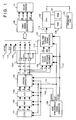
- Fig. 1 is a block diagram illustrating the signal processing of the color image reading apparatus of the first embodiment of the present invention.
- the color image reading apparatus shown in Fig. 1 connects to a color printer 10.
- numeral 101 is a color sensor comprising CCD line sensor of R (red), G (green), B (blue), numeral 102 is an analog amplifier, numeral 103 is an A/D convertor, and numeral 104 is a shading correcting circuit for correcting dispersions of brightness at the reading position of the image signal.
- Numeral 106 is a color-space matching judgment circuit for calculating the degree of similarity between the color distribution of the image data R, G, and B obtained by reading an original and that of the data obtained from the test original or specific originals, such as bank notes or securities, in a three-dimensional color space in real-time. Brightness and color distortion according to the position of the original are corrected by using the color signal after the shading correction by the shading correction circuit 104 and a judgment of the degree of similarity in the color space can be accurately performed regardless of the position where the original is placed.
- Fig. 10 illustrates the relationship between the position of the specific original on the platen and recognition zone. In Fig.
- the recognition zone is located at xb0 - xb1 in the main scanning direction and yb0 - yb1 in the subordinate scanning direction.
- Numeral 105 is a print-signal generation circuit which converts input color signals of R (red), G (green), B (blue) read by the color sensor 101 into signals of Y (yellow), M (magenta), C (cyan), Bk (black).
- Numeral 107 is a real-time change signal generation circuit which generates a real-time change signal f (signal line 113). The input image signal is modulated by the real-time change signal f. For example, where the original on the platen is identified as a specific original, a bitch-black image can be formed by outputting a maximum value with the RGB signals in real-time.
- Numeral 108 is a read-synchronous signal generation circuit which generates a main scanning direction interval signal HSYNC (signal line 109), primary clock signal CLK (signal line 110), and interval signal VSYNC (signal line 112) indicating the effective zone in the subordinate scanning direction.
- Numeral 120 is a CPU which controls the apparatus and control unit 121, and particularly making it possible to display the test result of the judging function.
- Numeral 127 is a ROM which stores a program to operate the CPU 120.
- Numeral 128 is a RAM used as a work area of various programs. The ROM 127 stores the program for testing the judging function to follow the flowchart of Fig. 17 (which will described later).
- Numeral 1601 is a modifying circuit which modifies the RGB signals from the shading circuit 104 by the real-time change signal f indicating the result of judgment whether the original is a specific original.
- Fig. 2 is a block diagram illustrating the construction of the color-space matching judgment circuit 106 according to the first embodiment.
- Fig. 9 is a diagram showing the color distribution formed from the specific original in the R-G-B three-dimensional color space and ROM 204 which stores a set of the input signals RGB and 1-bit judging signal as data of the color distribution in the first embodiment.
- numeral 201 is a R (red) signal which is the data of the five higher order address bits and come from the eight-bit R signal from the shading correcting circuit 104.
- numeral 202 is a five-bit G (green) signal and numeral 203 is a five-bit B (blue) signal.
- Numeral 204 is a ROM which beforehand stores data relating to the colors of a plurality of types (eight types) of specific originals. That is, the data on the eight types of the color distribution shown in Fig. 9 are stored in a single ROM.
- the test original and each type of the specific originals stored as data in the ROM 204 is hereinafter referred to as a "prohibited master".
- the R, G, B signals 201 ⁇ 203 are inputted as addresses A0 through A14. Subsequently, a judgment signal (1 bit ⁇ 8 types) indicating whether the inputted R, G, B signals 201 ⁇ 203 coincide with the colors of the plurality of the prohibited masters is outputted from the output terminals D0 ⁇ D7 as data R0 ⁇ R7.
- the prohibited master corresponding to the "test original" described later is included in the eight types of the prohibited masters.
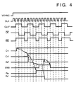
- Numeral 205 is a timing signal generation circuit for generating a timing signal shown in Fig. 4.
- Numeral 206 is a clock signal (CLK'') obtained by frequency division of the CLK signal by four.
- Numeral 207 is a signal to control a write-enable-terminal of an SRAM 209 and numeral 208 is a signal to control an output-enable-terminal of the SRAM 209.
- the data stored in the ROM 204 includes the information related to the colors of the eight types of the prohibited master as shown in Fig. 9. If an input color of the original coincides with the color of the prohibited master, "1" is respectively outputted to output terminals D0 ⁇ D7 as color judgment signals x0 ⁇ x7. While if they do not coincide, "0" is respectively outputted to the output terminals D0 ⁇ D7.
- the color judgment signals "x0 ⁇ x7" are judgment signals respectively corresponding to the eight types of the prohibited masters A through H (obtained from the test original A and specific originals B through H).
- Numerals 271, 272 are selectors
- numeral 270 is an address generator
- numerals 220 ⁇ 227 are smoothing circuits
- numerals 240 ⁇ 247 are color-space judging circuit.
- Fig. 11 is a diagram illustrating the color distribution of the prohibited master A (which contains the same data as that of the "test original" 1801 for testing the judging function) in the color space used in the first embodiment.
- Fig. 18 is a diagram for describing the test original in the first embodiment.
- Fig. 13 is a diagram showing the data, stored in the SRAM 209, on the relationship between the colors of the original on the platen and those of the eight types of the prohibited masters, and the relationship of the bit position of the SRAM 209.
- each of the judgement information R0 ⁇ R7 (signal lines 250 ⁇ 257) relating to the colors of the eight types of the prohibited masters is outputted from the output terminals D0 ⁇ D7 to the inputted image data in parallel.
- the color information (prohibited master A) which is stored in the address bit 0 (corresponding to D0) of the SRAM 209 is the color information relating to the test original 1801 shown in Figs. 11 and 18.
- the smoothing circuits 220 ⁇ 227 perform a smoothing calculation shown in Figs. 7 and 8 by using the signals of the color judging signals x0 ⁇ x7 (signal lines 210 ⁇ 217).
- Fig. 7 is a block diagram illustrating the construction of the smoothing circuits 220 ⁇ 227 in the first embodiment.
- numerals 701 and 702 are multipliers
- numeral 703 is an adder
- numeral 704 is a latch circuit
- numeral 705 is a comparator.
- Figs. 8A and 8B shows the relationship between the input x i and output value y i in the first embodiment. As shown in these figures, if the input value x i continues (Fig. 8A), the value y i is increased (Fig. 8B).
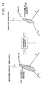
- Fig. 14 is a diagram for conceptually describing the judgement of the degree of similarity of the color distribution of the input color image in the color space and color distribution of the prohibited master.
- the degree of similarity of the prohibited master data in the R, G, B color space and input color signal is calculated in real-time and the color-space similarity judgment signals MK0 ⁇ MK7 (signal lines 260 ⁇ 267) are calculated.
- Fig. 3 is a block diagram illustrating the construction of the color-space judging circuit according to the first embodiment.
- numeral 301 is a 10-bit counter
- numeral 302 is a comparator
- numeral 303 is a register
- numerals 351 ⁇ 354 are inverters
- numerals 361 ⁇ 365 are D-flip flops
- numeral 366 is an AND gate
- numerals 367, 368 are NAND gates
- numeral 369 is a NOR gate
- numeral 370 is a buffer.
- the color-space similarity judgment signal MK0 ⁇ MK7 (signal lines 260 ⁇ 267) is set to "1".
- the selectors 271 and 272 clears the SRAM 209 to "0" when the subordinate scanning interval signal VSYNC (signal line) 112 is "0" (LOW).
- the address generator 270 is a circuit for sequentially generating all addresses of the SRAM 209. When the interval signal VSYNC (signal line) 112 is at LOW, the SRAM 209 is cleared to "0" in accordance with the address signal generated by the address generator 270.
- Figs. 4A and 4B are timing charts relating to reading/writing from/on the SRAM 209.
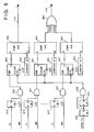
- Fig. 5 is a block diagram illustrating the construction of the real-time change signal generation circuit 107 according to the first embodiment.
- numerals 113 and 114 are signal lines
- numerals 500 ⁇ 507 are 16-bit counters
- numerals 510 ⁇ 517, 550, 551 are D-flip flops
- numerals 530 ⁇ 537 are AND gates
- numeral 552 is a NAND gate
- numerals 520 ⁇ 527 are registers
- numerals 540 ⁇ 547 are comparators
- numerals 553 is an OR gate.
- the real-time change signal f (signal line 113) is set to "1" (HIGH). It should be noted that the data of the prohibited master A is not used to form the real-time signal f.
- Fig. 12 shows the distribution of the prohibited master B in the color space.
- test original judgment signal J (signal line 114) is set to "1" (HIGH).
- Fig. 6 is a block diagram illustrating the construction of the print-signal generation circuit according to the first embodiment.
- numeral 610 is a log converter and numeral 611 is a masking-UCR circuit.
- the log converter 610 converts the R, G, B signals outputted from the correction circuit 1601 to the density signals, Y, M, C, Bk.
- the masking-UCR circuit 611 implements masking and under color removal based upon a density signal and the result is outputted to the color printer 10.
- Fig. 15 is a top plan view illustrating an operational surface of the operation unit 121 according to the first embodiment.
- the operation unit 121 shown in Fig. 15 comprises a test key 1510 for designating to test the original judgment, read-key 1511 for designating reading the original, and liquid crystal display (LCD) 1512 for displaying various messages in the process of testing.
- test key 1510 for designating to test the original judgment
- read-key 1511 for designating reading the original
- LCD liquid crystal display
- the judgement (test for the judging function) using the prohibited master A is started in a judgment function test mode.
- the read-key 1511 is pressed, the original is read in an ordinary copy mode.
- Fig. 16 is a diagram illustrating an example of the first embodiment
- Fig. 17 is a flowchart for describing the operation by the CPU 120 according to the first embodiment.
- the apparatus waits for the moment when the test key 1510 on the operation unit 121 shown in Fig. 15 is pressed by an operator.
- the operator places the test original 1801 on the platen beforehand.
- step S1703 the operation for reading the test original is executed.
- the judgment function test mode it is judged whether the judging function is properly operating by comparing the color distribution of the image data obtained by reading the test original by the color sensor 101 and that of the prohibited master A stored in the ROM 204 beforehand.
- ROM 204 and SRAM 209 are designed so as to deal with the data both of the prohibited master A used in the test mode and prohibited masters B ⁇ H used in the ordinal copy mode, they do not have to be designed separately for the test mode and ordinal copy mode, resulting in simplifying the construction. Furthermore, in the test mode, it is possible to judge whether the functions of the ROM and SRAM are properly operated.
- the judging function can be easily tested by testing the image judging function for detecting the specific original.
- CCD characteristics, image signal, analog processing characteristics can be tested by using the test original and testing relating to the function of the specific original detection can be performed sufficiently.
- the second embodiment is described below.
- the first embodiment is the example where the present invention is applied to the copier. However, it does not impose a limitation upon the present invention.
- the present invention can be applied to the image scanner connecting to a host computer as described below in the second embodiment.
- Fig. 19 is a block diagram illustrating the construction of the color image reading apparatus according to the second embodiment.
- Numeral 1901 denotes a computer.
- the circuits and signals shown in Fig. 19 which are substantially the same as those in Fig. 1 are designated by reference numerals of the numerals of Fig. 1 with an apostrophe ' and descriptions of these corresponding components are deleted.
- the first embodiment differs from the third embodiment in comprising the print-signal generation circuit 105.
- the print-signal generation circuit 105 is necessary. Accordingly, if the color image reading apparatus is designated to output to the computer 1901, a simple arrangement which does not comprise the print-signal generation circuit 105 can be adopted.
- the third embodiment is described below.
- the result of the test in the judgment function is displayed by the message and informed to the operator.
- this does not impose a limitation upon the present invention.
- it can be arranged so that the CPU controls not begin the reading operation until the test in the judging function ends and finds out that the function is operated in the ordinary copy mode.
- Fig. 20 is a block diagram illustrating the construction of the color image reading apparatus according to the third embodiment.
- Numeral 115 is a signal line and numeral 2001 is an OR gate.
- the circuits and signals shown in Fig. 20 which are substantially the same as these in Fig. 1 are designated by reference numerals of the numerals of Fig. 1 with a double-apostorphes '' and descriptions of these corresponding components are deleted.
- the third embodiment of Fig. 20 differs from the first embodiment of Fig. 1 in that, in the OR gate 2001, the modifying circuit 1601'' executes a correction in accordance with a signal obtained by taking an OR of a real-time change signal f and external control signal t, that is, a signal obtained by processing the result of whether the original to be copied is the specific original by the external control signal control signal t.
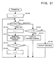
- Fig. 21 is a flowchart for describing the operation by the CPU 120'' according to the third embodiment.
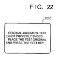
- Fig. 22 is a diagram illustrating an example of display according to the third embodiment.
- the external control signal t (signal line 115) is set to "1" (HIGH) by the CPU'' when the power of the reading apparatus is turned on.
- step S2101 when the test key (corresponding to the test key 1510) is pressed, the processes from steps S2102 ⁇ S2105 are performed, and when the read key (corresponding to the read key 1511) is pressed, the processes from steps S2106 ⁇ S2108 are performed.
- step S2101 When the test key (corresponding to the test key 1510) is pressed, at step S2101, the external control signal t (signal line 115) is set to "1" (HIGH).
- the test original is read.
- the function of the judging operation is assured by not transmitting the image signal to the printer until the test in the judging function ends properly.
- the present invention can be applied to a system constituted by a plurality of devices, or to an apparatus comprising a single device. Furthermore, it goes without saying that the invention is applicable also to a case where the object of the invention is attained by supplying a program to a system or apparatus.
- thermosensitive-transfer printer other than a laser bean printer can be used as image output means.
- a host computer video camera, still-video camera, and film reader for reading color films other than the image scanner which scans the original by the CCD sensor can be used as input means.
Landscapes
- Engineering & Computer Science (AREA)
- Multimedia (AREA)
- Signal Processing (AREA)
- Health & Medical Sciences (AREA)
- Biomedical Technology (AREA)
- General Health & Medical Sciences (AREA)
- Computer Security & Cryptography (AREA)
- Computer Vision & Pattern Recognition (AREA)
- Human Computer Interaction (AREA)
- Facsimile Image Signal Circuits (AREA)
- Image Analysis (AREA)
- Image Processing (AREA)
- Color Image Communication Systems (AREA)
Applications Claiming Priority (2)
| Application Number | Priority Date | Filing Date | Title |
|---|---|---|---|
| JP04389292A JP3260801B2 (ja) | 1992-02-28 | 1992-02-28 | 画像処理装置およびそのテスト方法、並びに、判定回路 |
| JP43892/92 | 1992-02-28 |
Publications (2)
| Publication Number | Publication Date |
|---|---|
| EP0558341A1 true EP0558341A1 (de) | 1993-09-01 |
| EP0558341B1 EP0558341B1 (de) | 1998-10-14 |
Family
ID=12676359
Family Applications (1)
| Application Number | Title | Priority Date | Filing Date |
|---|---|---|---|
| EP93301469A Expired - Lifetime EP0558341B1 (de) | 1992-02-28 | 1993-02-26 | Bildverarbeitungsgerät |
Country Status (5)
| Country | Link |
|---|---|
| US (1) | US5784483A (de) |
| EP (1) | EP0558341B1 (de) |
| JP (1) | JP3260801B2 (de) |
| CA (1) | CA2090449C (de) |
| DE (1) | DE69321500T2 (de) |
Cited By (1)
| Publication number | Priority date | Publication date | Assignee | Title |
|---|---|---|---|---|
| EP1349362A3 (de) * | 2002-03-29 | 2004-12-22 | Fuji Photo Film Co. Ltd. | Diagnostikverfahren für Bildverarbeitung |
Families Citing this family (4)
| Publication number | Priority date | Publication date | Assignee | Title |
|---|---|---|---|---|
| JP3762124B2 (ja) | 1997-12-26 | 2006-04-05 | キヤノン株式会社 | 画像処理装置および画像処理方法およびコンピュータが読み出し可能なプログラムを格納した記憶媒体 |
| JP2000134466A (ja) * | 1998-10-21 | 2000-05-12 | Murata Mach Ltd | 画像処理装置 |
| JP4646419B2 (ja) * | 2001-02-23 | 2011-03-09 | キヤノン株式会社 | インクジェット記録装置及びインクジェット記録装置の制御方法 |
| JP2003067805A (ja) * | 2001-08-28 | 2003-03-07 | Hitachi Ltd | 紙葉の真偽鑑別装置 |
Citations (1)
| Publication number | Priority date | Publication date | Assignee | Title |
|---|---|---|---|---|
| EP0463804A2 (de) * | 1990-06-22 | 1992-01-02 | Canon Kabushiki Kaisha | Vorrichtung und Verfahren zum Verarbeiten von Bildern |
Family Cites Families (8)
| Publication number | Priority date | Publication date | Assignee | Title |
|---|---|---|---|---|
| US3713097A (en) * | 1971-05-14 | 1973-01-23 | Ibm | Test bit pattern generator for pattern recognition machines |
| US4908873A (en) * | 1983-05-13 | 1990-03-13 | Philibert Alex C | Document reproduction security system |
| US4881268A (en) * | 1986-06-17 | 1989-11-14 | Laurel Bank Machines Co., Ltd. | Paper money discriminator |
| KR910001269B1 (ko) * | 1986-07-11 | 1991-02-26 | 로우렐 뱅크 머시인 가부시끼가이샤 | 광센서 조정용 장치 |
| US5321470A (en) * | 1988-05-13 | 1994-06-14 | Canon Kabushiki Kaisha | Apparatus with anti-forgery provision |
| SG120852A1 (en) * | 1989-02-10 | 2006-04-26 | Canon Kk | Apparatus for image reading or processing |
| US5227871A (en) * | 1990-11-30 | 1993-07-13 | Canon Kabushiki Kaisha | Image processing apparatus capable of discriminating a predetermined image |
| US5335291A (en) * | 1991-09-20 | 1994-08-02 | Massachusetts Institute Of Technology | Method and apparatus for pattern mapping system with self-reliability check |
-
1992
- 1992-02-28 JP JP04389292A patent/JP3260801B2/ja not_active Expired - Fee Related
-
1993
- 1993-02-26 EP EP93301469A patent/EP0558341B1/de not_active Expired - Lifetime
- 1993-02-26 CA CA002090449A patent/CA2090449C/en not_active Expired - Lifetime
- 1993-02-26 DE DE69321500T patent/DE69321500T2/de not_active Expired - Lifetime
-
1994
- 1994-12-13 US US08/355,118 patent/US5784483A/en not_active Expired - Lifetime
Patent Citations (1)
| Publication number | Priority date | Publication date | Assignee | Title |
|---|---|---|---|---|
| EP0463804A2 (de) * | 1990-06-22 | 1992-01-02 | Canon Kabushiki Kaisha | Vorrichtung und Verfahren zum Verarbeiten von Bildern |
Cited By (1)
| Publication number | Priority date | Publication date | Assignee | Title |
|---|---|---|---|---|
| EP1349362A3 (de) * | 2002-03-29 | 2004-12-22 | Fuji Photo Film Co. Ltd. | Diagnostikverfahren für Bildverarbeitung |
Also Published As
| Publication number | Publication date |
|---|---|
| DE69321500T2 (de) | 1999-04-08 |
| US5784483A (en) | 1998-07-21 |
| CA2090449C (en) | 1999-04-13 |
| JP3260801B2 (ja) | 2002-02-25 |
| CA2090449A1 (en) | 1993-08-29 |
| EP0558341B1 (de) | 1998-10-14 |
| DE69321500D1 (de) | 1998-11-19 |
| JPH05244413A (ja) | 1993-09-21 |
Similar Documents
| Publication | Publication Date | Title |
|---|---|---|
| EP0733958B2 (de) | Bildverarbeitungsgerät | |
| US5287204A (en) | Image recognition apparatus for judging between monochromic and color originals | |
| JP3517757B2 (ja) | 画像処理装置 | |
| EP0800123B1 (de) | Verfahren und Vorrichtung zur Bilderkennung und Kopier- und Abtastgerät hierfür | |
| US6185404B1 (en) | Image processing apparatus and method for generating a control signal based on a discrimination of whether an input image includes a specific image | |
| CA2090581C (en) | Image processing method and apparatus | |
| CA2090753C (en) | Image processing with anti-forgery provision | |
| US6621922B2 (en) | Image processing system and electronic apparatuses | |
| JPH07264419A (ja) | 画像処理装置 | |
| US5784483A (en) | Image processing apparatus | |
| EP0522768B1 (de) | Bildprozessor | |
| US6346989B1 (en) | Image processing apparatus and method | |
| JP3247446B2 (ja) | 画像処理装置及び画像処理方法 | |
| JP3267341B2 (ja) | 画像処理装置及び画像処理方法 | |
| JP3272739B2 (ja) | 画像処理装置およびその方法 | |
| JPH07182518A (ja) | 画像処理方法及びその装置 | |
| JP3313738B2 (ja) | 画像処理装置及び画像処理方法 | |
| JP3245154B2 (ja) | 画像処理装置 | |
| JP3614229B2 (ja) | 画像処理装置 | |
| JPH0522593A (ja) | 画像処理装置 | |
| JP3109984B2 (ja) | カラー画像処理装置 | |
| JPH07262377A (ja) | カラー画像処理方法及びその装置 | |
| JPH0944669A (ja) | 画像処理方法及びその装置 | |
| JPH05344331A (ja) | 画像処理装置 | |
| JPH07175923A (ja) | 画像処理方法及びその装置 |
Legal Events
| Date | Code | Title | Description |
|---|---|---|---|
| PUAI | Public reference made under article 153(3) epc to a published international application that has entered the european phase |
Free format text: ORIGINAL CODE: 0009012 |
|
| AK | Designated contracting states |
Kind code of ref document: A1 Designated state(s): DE FR GB IT NL |
|
| 17P | Request for examination filed |
Effective date: 19940118 |
|
| 17Q | First examination report despatched |
Effective date: 19960122 |
|
| GRAG | Despatch of communication of intention to grant |
Free format text: ORIGINAL CODE: EPIDOS AGRA |
|
| GRAG | Despatch of communication of intention to grant |
Free format text: ORIGINAL CODE: EPIDOS AGRA |
|
| GRAG | Despatch of communication of intention to grant |
Free format text: ORIGINAL CODE: EPIDOS AGRA |
|
| GRAH | Despatch of communication of intention to grant a patent |
Free format text: ORIGINAL CODE: EPIDOS IGRA |
|
| GRAH | Despatch of communication of intention to grant a patent |
Free format text: ORIGINAL CODE: EPIDOS IGRA |
|
| GRAA | (expected) grant |
Free format text: ORIGINAL CODE: 0009210 |
|
| AK | Designated contracting states |
Kind code of ref document: B1 Designated state(s): DE FR GB IT NL |
|
| REF | Corresponds to: |
Ref document number: 69321500 Country of ref document: DE Date of ref document: 19981119 |
|
| ET | Fr: translation filed | ||
| PLBE | No opposition filed within time limit |
Free format text: ORIGINAL CODE: 0009261 |
|
| STAA | Information on the status of an ep patent application or granted ep patent |
Free format text: STATUS: NO OPPOSITION FILED WITHIN TIME LIMIT |
|
| 26N | No opposition filed | ||
| REG | Reference to a national code |
Ref country code: GB Ref legal event code: IF02 |
|
| PGFP | Annual fee paid to national office [announced via postgrant information from national office to epo] |
Ref country code: NL Payment date: 20090217 Year of fee payment: 17 |
|
| PG25 | Lapsed in a contracting state [announced via postgrant information from national office to epo] |
Ref country code: IT Free format text: LAPSE BECAUSE OF NON-PAYMENT OF DUE FEES Effective date: 20080226 |
|
| PGFP | Annual fee paid to national office [announced via postgrant information from national office to epo] |
Ref country code: IT Payment date: 20090205 Year of fee payment: 16 |
|
| PGFP | Annual fee paid to national office [announced via postgrant information from national office to epo] |
Ref country code: FR Payment date: 20090223 Year of fee payment: 17 |
|
| REG | Reference to a national code |
Ref country code: NL Ref legal event code: V1 Effective date: 20100901 |
|
| REG | Reference to a national code |
Ref country code: FR Ref legal event code: ST Effective date: 20101029 |
|
| PG25 | Lapsed in a contracting state [announced via postgrant information from national office to epo] |
Ref country code: NL Free format text: LAPSE BECAUSE OF NON-PAYMENT OF DUE FEES Effective date: 20100901 Ref country code: FR Free format text: LAPSE BECAUSE OF NON-PAYMENT OF DUE FEES Effective date: 20100301 |
|
| PGFP | Annual fee paid to national office [announced via postgrant information from national office to epo] |
Ref country code: DE Payment date: 20110228 Year of fee payment: 19 |
|
| PGFP | Annual fee paid to national office [announced via postgrant information from national office to epo] |
Ref country code: GB Payment date: 20110224 Year of fee payment: 19 |
|
| GBPC | Gb: european patent ceased through non-payment of renewal fee |
Effective date: 20120226 |
|
| REG | Reference to a national code |
Ref country code: DE Ref legal event code: R119 Ref document number: 69321500 Country of ref document: DE Effective date: 20120901 |
|
| PG25 | Lapsed in a contracting state [announced via postgrant information from national office to epo] |
Ref country code: GB Free format text: LAPSE BECAUSE OF NON-PAYMENT OF DUE FEES Effective date: 20120226 |
|
| PG25 | Lapsed in a contracting state [announced via postgrant information from national office to epo] |
Ref country code: DE Free format text: LAPSE BECAUSE OF NON-PAYMENT OF DUE FEES Effective date: 20120901 |