EP0560393A1 - Mikroprozessor und Datenverarbeitungsanlage mit Registerspeicher - Google Patents
Mikroprozessor und Datenverarbeitungsanlage mit Registerspeicher Download PDFInfo
- Publication number
- EP0560393A1 EP0560393A1 EP93104091A EP93104091A EP0560393A1 EP 0560393 A1 EP0560393 A1 EP 0560393A1 EP 93104091 A EP93104091 A EP 93104091A EP 93104091 A EP93104091 A EP 93104091A EP 0560393 A1 EP0560393 A1 EP 0560393A1
- Authority
- EP
- European Patent Office
- Prior art keywords
- bank
- microprocessor
- register file
- address
- peripheral device
- Prior art date
- Legal status (The legal status is an assumption and is not a legal conclusion. Google has not performed a legal analysis and makes no representation as to the accuracy of the status listed.)
- Granted
Links
Images
Classifications
-
- G—PHYSICS
- G06—COMPUTING OR CALCULATING; COUNTING
- G06F—ELECTRIC DIGITAL DATA PROCESSING
- G06F12/00—Accessing, addressing or allocating within memory systems or architectures
- G06F12/02—Addressing or allocation; Relocation
-
- G—PHYSICS
- G06—COMPUTING OR CALCULATING; COUNTING
- G06F—ELECTRIC DIGITAL DATA PROCESSING
- G06F9/00—Arrangements for program control, e.g. control units
- G06F9/06—Arrangements for program control, e.g. control units using stored programs, i.e. using an internal store of processing equipment to receive or retain programs
- G06F9/46—Multiprogramming arrangements
- G06F9/461—Saving or restoring of program or task context
- G06F9/462—Saving or restoring of program or task context with multiple register sets
Definitions
- This invention relates to a microprocessor, which has a bank structure, and a data processing system in which said microprocessor is incorporated.
- this invention relates to a microprocessor which has a structure to conduct data processings by connecting a particular memory (bank RAM), which is mapped on an address map of a data processing system, with a group of registers contained in this microprocessor, and the data processing system itself.
- MPU general purpose registers in the microprocessor
- the word 'bank' means a group of registers which are mainly used for operations in the MPU.
- the number of banks for one task is determined according to the MPU program.
- a group of registers, that is, a bank is switched into another.
- the number of banks incorporated in the MPU is limited according to the chip size of this MPU. Therefore, many banks cannot be incorporated in the MPU.
- a system having an external memory In order to increase the number of banks which can be utilized by the MPU, a system having an external memory is proposed. In this system, banks are saved in areas of a special memory (bank RAM) mapped on the address map of this MPU. When a particular bank saved in a certain area of the bank RAM is recalled by the MPU, the data in said area is taken out from the memory and loaded on the bank in the MPU. In this case, if the data transfer between a bank inside the MPU and the bank RAM outside the MPU is carried out through external buses, the MPU must stop for a long time until the bank exchange is completed. Therefore, the data transfer between the bank in the MPU and the bank RAM is conducted through a dedicated bus at a high speed.
- bank RAM special memory
- bank exchange between the bank RAM outside the MPU and the bank in the MPU is conducted through the dedicated high speed bus, instead of external buses.
- the device does not recognize whether the content in the accessed area of the bank RAM is now in use by the MPU as a bank or not. Only the MPU recognizes whether the content accessed by said peripheral device is now in use by itself, or not. Accordingly, when the MPU uses the bank RAM as a bank, the peripheral device is able to access only the old information of the bank RAM. In other words, when the MPU uses the bank RAM as a bank, the Peripheral device cannot access the newest information in the bank RAM.
- This invention has been made to overcome the above mentioned disadvantage of the prior art microprocessor and data processing system.
- the first objective of the present invention is to provide a microprocessor which can be incorporated in a data processing system having a bank structure and has a function to effectively control the data transfer between itself and an external memory, in order that a peripheral device is able to access the newest information in said external memory.
- Another objective of the present invention is to provide a data processing system having said microprocessor and a memory, the system in which the data transfer inside this system can be controlled effectively so that a peripheral device in this system can access the newest information in said memory.
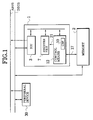
- the first feature of the present invention provides a microprocessor which is comprised of the following as shown in Fig. 1: a register file 7; and means 12 for controlling the data transfer between said register file 7 and an external memory 2 which is connected to the present microprocessor 1 itself through a dedicated bus 17; wherein said means 12 has a function to control a data transfer between said register file 7 and a peripheral device 30, which is connected to said external memory 2 through an external data bus DBUS, or the microprocessor 1 itself, instead of a data transfer between said external memory 2 and peripheral device 30 or the microprocessor, when a particular address area in said external memory 2, the area which corresponds to the bank now in use in register file 7, is accessed by said peripheral device 30 or the microprocessor 1 itself through said external data bus DBUS.
- control means 12 has a pointer 10 to hold a first address of an memory area in which the bank now in use in register file 7 is stored.
- control means 12 has an adder-subtracter 25 (or an adder, shown in Fig. 2) in addition to said pointer 10, so as to compare the address information input, from peripheral device 30 or microprocessor 1, with the content in said pointer 10.
- the fourth feature of the present invention provides a data processing system, which is comprised of the following as shown in Fig. 1: a microprocessor 1 which has the structure having said first, second, or third feature; memory 2 which is mapped on the address map of this data processing system; at least one peripheral device 30; data bus DBUS which connects among microprocessor 1, peripheral device 30, and memory 2; address bus ABUS which connects between microprocessor 1 and peripheral device 30; and dedicated bus 17 which connects microprocessor 1 with memory 2.
- control means 12 has a function to find if peripheral device 30 or microprocessor 1 itself has accessed said address area, which corresponds to the bank now in use, in said memory 2 or not.
- control means 12 finds that the accessed area in memory 2 corresponds to the address area in which the bank now in use is stored, it controls a data transfer between register file 7 and peripheral device 30 or microprocessor 1, instead of controlling a data transfer between memory 2 and peripheral device 30 or microprocessor 1. This is because the newest information concerning about the accessed area in memory 2 is now in said register file.
- control means 12 finds that the accessed area in memory 2 does not correspond to said address area in which the bank now in use in register file 7 is stored, it controls a data transfer between memory 2 and peripheral device 30 or microprocessor 1 itself.
- peripheral device 30 or the microprocessor 1 can always obtain the newest information concerning about the accessed area in memory 2, even in the case where the area is used as the bank now in use in register file 7.
- pointer 10 holds the first address of an memory area in which the bank now in use in register file is stored. Therefore, by comparing the address information, accessed by peripheral device 30 or microprocessor 1, with the content in said pointer 10, control means 12 can easily find if said address information corresponds to said address area, in which the bank now in use in register file is stored, or not. When it corresponds to said address area, means 12 controls a data transfer between register file 7 and peripheral device 30 or microprocessor 1, instead of controlling a data transfer between memory 2 and peripheral device 30 or microprocessor 1.
- control means 12 can easily find if said address information corresponds to said address area in which the bank now in use in register file 7 is stored.
- memory 2 is combined with register file 7 contained in microprocessor 1, so as to operate register file 7 as a bank.
- the data transfer between register file 7 and memory 2 is controlled through dedicated bus 17, so that the data transfer can be controlled at a high speed.
- microprocessor 1 has a function to find if they have accessed a particular area in said memory 2, the area which is now in use as a bank in said register 7.
- peripheral device 30 or microprocessor 1 controls the data transfer between said register file 7 and peripheral device 30 or microprocessor 1, instead of controlling the data transfer between memory 2 and peripheral device 30 or microprocessor 1. So, peripheral device 30 or microprocessor 1 can always access the newest information in memory 2, even in the case where the accessed area is now in use as a bank in register file 7.
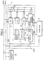
- Fig. 2 shows the structure of a microprocessor according to one embodiment of the present invention, and a data processing system in which said microprocessor is incorporated.
- the data processing system is comprised of a microprocessor (referred to as MPU, below) 1, bank RAM 2, an external address bus ABUS, an external data bus DBUS, an external control bus CBUS, and at least one peripheral device 30.
- MPU 1 is connected with said buses as shown in Fig. 2.
- bank RAM 2 is connected with data bus DBUS.
- This bank RAM 2 is also connected with MPU 1 through dedicated high-speed bus 17 and bank RAM address control signal 18.
- at least one peripheral device 30, such as an I/O, a ROM, and a RAM, each of which is mapped on the address map of MPU 1 through external address bus ABUS, data bus DBUS, and control bus CBUS, is connected to MPU 1.
- MPU 1 is comprised of the following: a bus interface unit (BIU) 3; an instruction queue 4; a micro-ROM 5; an arithmetic and logical unit (ALU) 6; a register file (REG) 7; a bank interface unit 8; and a bank control unit 9.
- BIU bus interface unit
- ALU arithmetic and logical unit
- REG register file
- bank interface unit 8 a bank control unit 9.
- the signal connection among bus interface unit 3, instruction queue 4, micro-ROM 5, arithmetic and logical unit 6, and register file 7 is very complicated. However, this connection is not related to the main purpose of this invention, so that it is shown briefly.
- Bank RAM 2 is connected with bus interface unit 8 in MPU 1 through dedicated high-speed bus 17. However, bank RAM 2 is controlled by MPU 1 or peripheral device 30 through bank RAM address control signal 18 which is output from bank control unit 9 in MPU 1. Bank RAM 2 is also connected with external data bus DBUS in order to exchange data with MPU 1 or peripheral device 30, in the similar manner as that of a ROM and a RAM (not shown) which are mapped on the address map of the data processing system.
- Bank interface unit 8 contains a current bank pointer (CBP) 10 and a previous bank pointer (PBP) 11.
- Current bank pointer 10 holds the data (or the address itself) indicating a particular address area of bank RAM 2, the area which is now in use as a bank in register file 7.
- previous bank pointer (PBP) 11 holds the data (or the address itself) indicating another particular address area of bank RAM 2, the area which is the return area of another bank to be recalled by register file 7 at the completion of the task under operation.
- Bank control unit 9 contains an adder-subtracter 25 which controls arithmetic operations between the data from current bank pointer 10 and external address bus ABUS. These operations in adder-subtracter 25 are carried out in order to find if peripheral device 30 accesses the address area of the bank, now in use by MPU 1, in bank RAM 2, as well as to transfer data between register file 7 and bank RAM 2 at a high speed using dedicated bus 17, which has the maximum data width between register file 7 and bank RAM 2. Such a high-speed data transfer takes place when bank exchange between register file 7 and bank RAM 2 is required. Because a subtraction can be carried out by an addition, an adder is used instead of said adder-subtracter 25.
- register file 7 transfers data with MPU 1 itself, or peripheral device 30 through bank interface unit 3, which is connected with register file 7 via internal X bus 14, Y bus 15, and Z bus 16.
- bank interface unit 8 the data transfer between bank RAM 2 and register file 7 is controlled through bank interface unit 8.
- peripheral device 30 the data transfer between external data bus DBUS and register file 7 is controlled through bank interface unit 8.
- bank RAM 2 In an ordinary occasion, the data transfer between bank RAM 2 and external data bus DBUS is executed under the control by bank RAM address control signal 18 from bank control unit 9. This control by signal 18 is based on instructions obtained from peripheral device 30 through external address bus ABUS and control bus CBUS.
- Bank RAM 2 also has a function to connect external DBUS with dedicated high speed bus 17, when said instructions obtained through external address bus ABUS and control bus CBUS are concerned about the return area of a bank in bank RAM 2, the bank which is now in use in register file 7.
- Bank RAM 2 has another function to exchange data with register file 7 through dedicated high speed bus 17, when MPU 1 itself requires high-speed bank exchange.
- the process (2) or (3) is executed when a peripheral device accesses bank RAM 2.
- either one of said operations is executed when an address to specify bank RAM 2 is supplied on external address bus and when signals contained in external control bus CBUS, such as a bus start signal, a chip select signal, and a data read-write signal, become active.
- both current bank pointer 10 and previous bank pointer 11 have 8 bits
- register file 7 has 32 bytes
- external address bus ABUS has 24 bits (address 000000H to FFFFFFH, H means the hexadecimal representation)
- the address map of bank RAM 2 has 0 to 2K bytes (address 000000H to 0007FFH)
- external data bus DBUS has 16 bits
- dedicated high-speed bus 17 has 64 bits.
- external control bus CBUS has a bus start signal to indicate the beginning of a bus cycle, a read-write signal to indicate that data are input to or output from external data bus DBUS, and a chip select signal to activate a ROM or a RAM, which are provided around MPU 1.
- the 8 bit data which are obtained by shifting the 3 bits of current bank pointer 10 to the left, are set at the higher 8 bits, and the 3 bit data '000' are set at the lower 3 bits, thus providing 11 bit data. These data indicate the lower 11 bits of the first address of an address area in bank RAM 2, the area which corresponds to the bank now in use by MPU 1.
- the data transfer between register file 7 and bank RAM 2 for the exchange of banks is carried out as follows.
- the 8 bit data, which are obtained by shifting the 3 bits of current bank pointer 10 to the left, are incremented to produce 8 byte address signals. These address signals are supplied into bank RAM 2 through bank RAM address control signal 18. Then, the data are transferred four times by 64 bit width through dedicated high-speed bus 17 between bank RAM 2 and register file 7.
- the address for register file 7 is incremented four times by 8 bytes.
- the continuous data of bank RAM 2 beginning from said 11 bit address are loaded on the bank.
- Said 11 bit address data are produced as follows.
- the 8 bit data, which are obtained by shifting the 3 bits of current bank pointer 10 to the left, are set at the higher 8 bits, and the 3 bit data '000' are set at the lower 3 bits, thus providing said 11 bit address data.
- Bank control unit 9 in MPU 1 monitors the lower 11 bits of external address bus ABUS and external control bus CBUS.
- adder-subtracter 25 in bank control unit 9 conducts a subtraction between the higher 8 bits of the lower 11 bits of external address bus ABUS and the 8 bits of current bank pointer 10. If the result of said subtraction is between 0 to 3, it means that the content in bank RAM 2 accessed by the peripheral device is now in use in register file 7 as a bank. If the result is not between 0 to 3, the content in bank RAM 2 accessed by the peripheral device is not in use in register file 7.
- bank control unit 9 When the content in bank RAM 2 accessed by the peripheral device is not in use by MPU 1 as a bank, bank control unit 9 outputs the lower 11 bits of external address bus ABUS to bank RAM 2 without a change. Also, bank control unit 9 processes the bus start signal, read-write signal, and chip select signal contained in external control bus CBUS, and then, outputs the resulting signal as bank RAM address control signal 18. Thus, the content in bank RAM 2 is transferred into peripheral unit 30 through external data bus DBUS.
- bank control unit 9 outputs register file address control signal 21 to register file 7.
- This signal 21 is produced from external control bus CBUS and a 5 bit address signal, in which the higher 2 bits of the operation result in adder-subtracter 25 are placed in its higher part, and the lower 3 bits of external address bus ABUS are placed in its lower part.
- bank interface unit 8 connects the data bus from register file 7 with dedicated high-speed bus 17.
- bank control unit 9 also controls bank RAM 2 using bank RAM address control signal 18, so that dedicated high speed bus 17 is connected with external data bus DBUS.
- the bus width of dedicated high-speed bus 17 deferes from that of external data bus DBUS. Accordingly, in order to connect high-speed bus 17 with data bus DBUS, the essential 16 bits data are taken out from dedicated high-speed bus 17 using the higher 2 bits among the lower 3 bits of external address bus ABUS. Then, said 16 bit data are made to run on external data bus DBUS. In this case, the content in bank RAM 2 is not accessed at all.
- register file 7 is accessed instead of bank RAM 2.
- bank wait signal 23 notifies MPU 1 that register file 7 is now being accessed.
- the operation of MPU 1 is not influenced by said operation of the peripheral device.
- the data processing system of this embodiment stores, into current bank pointer 10, of information concerning about the first address of an address area in bank RAM 2, the area which corresponds to the bank now in use in register file 7.
- the content in current bank pointer 10 is, then, compared with the address information which is input from peripheral device 30, so as to find if peripheral device 30 accesses a particular area in bank RAM 2, the area which corresponds to the bank now in use in register file 7, or not.
- the area in bank RAM 2 accessed by peripheral device 30 is found to correspond to the address area of the bank now in use in register file 7, data access is executed for register file 7 instead of bank RAM 2.
- peripheral device can always access the newest information in bank RAM 2.
- control means contained in the microprocessor of this invention has a function to find if a peripheral device or the microprocessor itself accesses a particular area in an external memory, the area which corresponds to the bank now in use by this microprocessor itself, or not.
- the control means controls a data transfer between a register file (bank) and said peripheral device or the microprocessor itself, instead of a data transfer between said external memory (bank RAM) and said peripheral device or the microprocessor itself.
- the microprocessor itself or said peripheral device can access the newest information in said external memory, even in the case where said area, corresponding to the bank now in use by this microprocessor, is accessed by them.
- this invention can provide a microprocessor and a data processing system, in which the newest information in an external memory can be correctly and efficiently accessed by a peripheral device or the microprocessor itself.
Landscapes
- Engineering & Computer Science (AREA)
- Theoretical Computer Science (AREA)
- Software Systems (AREA)
- Physics & Mathematics (AREA)
- General Engineering & Computer Science (AREA)
- General Physics & Mathematics (AREA)
- Executing Machine-Instructions (AREA)
- Memory System (AREA)
Applications Claiming Priority (3)
| Application Number | Priority Date | Filing Date | Title |
|---|---|---|---|
| JP5373592 | 1992-03-12 | ||
| JP4053735A JP2568017B2 (ja) | 1992-03-12 | 1992-03-12 | マイクロプロセッサ及びそれを使用したデータ処理システム |
| JP53735/92 | 1992-03-12 |
Publications (2)
| Publication Number | Publication Date |
|---|---|
| EP0560393A1 true EP0560393A1 (de) | 1993-09-15 |
| EP0560393B1 EP0560393B1 (de) | 2000-06-21 |
Family
ID=12951088
Family Applications (1)
| Application Number | Title | Priority Date | Filing Date |
|---|---|---|---|
| EP93104091A Expired - Lifetime EP0560393B1 (de) | 1992-03-12 | 1993-03-12 | Mikroprozessor und Datenverarbeitungsanlage mit Registerspeicher |
Country Status (5)
| Country | Link |
|---|---|
| US (1) | US5561818A (de) |
| EP (1) | EP0560393B1 (de) |
| JP (1) | JP2568017B2 (de) |
| KR (1) | KR960012354B1 (de) |
| DE (1) | DE69328883T2 (de) |
Cited By (3)
| Publication number | Priority date | Publication date | Assignee | Title |
|---|---|---|---|---|
| EP0697651A3 (de) * | 1994-08-12 | 1997-07-23 | Nec Corp | Mikroprozessor mit Registerspeicher |
| GB2402759A (en) * | 2003-06-12 | 2004-12-15 | Advanced Risc Mach Ltd | Transferring data files between a register file and a memory |
| CN109144725A (zh) * | 2018-08-02 | 2019-01-04 | 北京达佳互联信息技术有限公司 | 文件处理方法、装置、电子设备及存储介质 |
Families Citing this family (2)
| Publication number | Priority date | Publication date | Assignee | Title |
|---|---|---|---|---|
| US5842041A (en) * | 1994-05-20 | 1998-11-24 | Advanced Micro Devices, Inc. | Computer system employing a control signal indicative of whether address is within address space of devices on processor local bus |
| US6003112A (en) * | 1997-06-30 | 1999-12-14 | Intel Corporation | Memory controller and method for clearing or copying memory utilizing register files to store address information |
Citations (2)
| Publication number | Priority date | Publication date | Assignee | Title |
|---|---|---|---|---|
| US4352157A (en) * | 1977-05-19 | 1982-09-28 | Tokyo Shibaura Electric Co., Ltd. | Data-processing apparatus having improved interrupt handling processor |
| US4905200A (en) * | 1988-08-29 | 1990-02-27 | Ford Motor Company | Apparatus and method for correcting microcomputer software errors |
Family Cites Families (10)
| Publication number | Priority date | Publication date | Assignee | Title |
|---|---|---|---|---|
| US3771137A (en) * | 1971-09-10 | 1973-11-06 | Ibm | Memory control in a multipurpose system utilizing a broadcast |
| FR2479532B1 (fr) * | 1980-04-01 | 1986-09-19 | Bull Sa | Procede et dispositif pour gerer les transferts d'informations entre un ensemble memoire et les differentes unites de traitement d'un systeme de traitement numerique de l'information |
| US4410944A (en) * | 1981-03-24 | 1983-10-18 | Burroughs Corporation | Apparatus and method for maintaining cache memory integrity in a shared memory environment |
| US4466098A (en) * | 1982-06-11 | 1984-08-14 | Siemens Corporation | Cross channel circuit for an electronic system having two or more redundant computers |
| JPS58225443A (ja) * | 1982-06-25 | 1983-12-27 | Nec Corp | 高速デ−タ処理装置 |
| US4858111A (en) * | 1983-07-29 | 1989-08-15 | Hewlett-Packard Company | Write-back cache system using concurrent address transfers to setup requested address in main memory before dirty miss signal from cache |
| US4928225A (en) * | 1988-08-25 | 1990-05-22 | Edgcore Technology, Inc. | Coherent cache structures and methods |
| US5131081A (en) * | 1989-03-23 | 1992-07-14 | North American Philips Corp., Signetics Div. | System having a host independent input/output processor for controlling data transfer between a memory and a plurality of i/o controllers |
| US5119485A (en) * | 1989-05-15 | 1992-06-02 | Motorola, Inc. | Method for data bus snooping in a data processing system by selective concurrent read and invalidate cache operation |
| US5263144A (en) * | 1990-06-29 | 1993-11-16 | Digital Equipment Corporation | Method and apparatus for sharing data between processors in a computer system |
-
1992
- 1992-03-12 JP JP4053735A patent/JP2568017B2/ja not_active Expired - Fee Related
-
1993
- 1993-03-11 KR KR1019930003598A patent/KR960012354B1/ko not_active Expired - Fee Related
- 1993-03-12 US US08/031,200 patent/US5561818A/en not_active Expired - Lifetime
- 1993-03-12 DE DE69328883T patent/DE69328883T2/de not_active Expired - Fee Related
- 1993-03-12 EP EP93104091A patent/EP0560393B1/de not_active Expired - Lifetime
Patent Citations (2)
| Publication number | Priority date | Publication date | Assignee | Title |
|---|---|---|---|---|
| US4352157A (en) * | 1977-05-19 | 1982-09-28 | Tokyo Shibaura Electric Co., Ltd. | Data-processing apparatus having improved interrupt handling processor |
| US4905200A (en) * | 1988-08-29 | 1990-02-27 | Ford Motor Company | Apparatus and method for correcting microcomputer software errors |
Non-Patent Citations (1)
| Title |
|---|
| MICROPROCESSORS AND MICROSYSTEMS, vol. 13, no. 9, November 1989, LONDON, GB; I.HAY ET AL 'TRON-Compatible 16/32-Bit Microprocessor' * |
Cited By (6)
| Publication number | Priority date | Publication date | Assignee | Title |
|---|---|---|---|---|
| EP0697651A3 (de) * | 1994-08-12 | 1997-07-23 | Nec Corp | Mikroprozessor mit Registerspeicher |
| US5713038A (en) * | 1994-08-12 | 1998-01-27 | Nec Corporation | Microprocessor having register file |
| GB2402759A (en) * | 2003-06-12 | 2004-12-15 | Advanced Risc Mach Ltd | Transferring data files between a register file and a memory |
| GB2402759B (en) * | 2003-06-12 | 2005-12-21 | Advanced Risc Mach Ltd | Data processing apparatus and method for transferring data values between a register file and a memory |
| CN109144725A (zh) * | 2018-08-02 | 2019-01-04 | 北京达佳互联信息技术有限公司 | 文件处理方法、装置、电子设备及存储介质 |
| CN109144725B (zh) * | 2018-08-02 | 2020-11-17 | 北京达佳互联信息技术有限公司 | 文件处理方法、装置、电子设备及存储介质 |
Also Published As
| Publication number | Publication date |
|---|---|
| JP2568017B2 (ja) | 1996-12-25 |
| JPH0635800A (ja) | 1994-02-10 |
| KR930020267A (ko) | 1993-10-19 |
| DE69328883T2 (de) | 2000-12-07 |
| US5561818A (en) | 1996-10-01 |
| EP0560393B1 (de) | 2000-06-21 |
| KR960012354B1 (ko) | 1996-09-18 |
| DE69328883D1 (de) | 2000-07-27 |
Similar Documents
| Publication | Publication Date | Title |
|---|---|---|
| EP0569969B1 (de) | Mikrocomputer mit Befehlsspeicher für Befehle zum Auslesen interner Bedingungen | |
| US4514808A (en) | Data transfer system for a data processing system provided with direct memory access units | |
| JP2829091B2 (ja) | データ処理システム | |
| JP2586833B2 (ja) | データプロセッサ | |
| US4715013A (en) | Coprocessor instruction format | |
| EP0511674A2 (de) | Ein-Chip-Mikrorechner | |
| US4729094A (en) | Method and apparatus for coordinating execution of an instruction by a coprocessor | |
| KR960705283A (ko) | 데이터 흐름 제어 및 다중 처리 유니트를 가진 상 압축 코프로세서(image compression coprocessor with data flow control and multiple processing units) | |
| US4731736A (en) | Method and apparatus for coordinating execution of an instruction by a selected coprocessor | |
| US4750110A (en) | Method and apparatus for executing an instruction contingent upon a condition present in another data processor | |
| JPH09330236A (ja) | マイクロプロセッサ及びその周辺装置 | |
| US5021991A (en) | Coprocessor instruction format | |
| US5757685A (en) | Data processing system capable of processing long word data | |
| US5125095A (en) | System using microprocessor address lines for coprocessor selection within a multi-coprocessor apparatus | |
| US4914578A (en) | Method and apparatus for interrupting a coprocessor | |
| US4758950A (en) | Method and apparatus for selectively delaying an interrupt of a coprocessor | |
| EP0139254A2 (de) | Vorrichtung und Verfahren für direkte Datenübertragung vom Speicher an das Peripheriegerät und vom Peripheriegerät an den Speicher | |
| US5481756A (en) | DMA controller mailing auto-initialize halting unit | |
| US4314332A (en) | Memory control system | |
| US5561818A (en) | Microprocessor and data processing system for data transfer using a register file | |
| US5742842A (en) | Data processing apparatus for executing a vector operation under control of a master processor | |
| EP0385136B1 (de) | Mikroprozessor, der mit einem Coprozessor zusammenarbeitet | |
| US4814977A (en) | Apparatus and method for direct memory to peripheral and peripheral to memory data transfers | |
| US4758978A (en) | Method and apparatus for selectively evaluating an effective address for a coprocessor | |
| EP0795827A1 (de) | Speicheranordnung und Verfahren zum Zugreifen auf die Speicher der Speicheranordnung |
Legal Events
| Date | Code | Title | Description |
|---|---|---|---|
| PUAI | Public reference made under article 153(3) epc to a published international application that has entered the european phase |
Free format text: ORIGINAL CODE: 0009012 |
|
| 17P | Request for examination filed |
Effective date: 19930312 |
|
| AK | Designated contracting states |
Kind code of ref document: A1 Designated state(s): DE GB |
|
| 17Q | First examination report despatched |
Effective date: 19970630 |
|
| GRAG | Despatch of communication of intention to grant |
Free format text: ORIGINAL CODE: EPIDOS AGRA |
|
| GRAG | Despatch of communication of intention to grant |
Free format text: ORIGINAL CODE: EPIDOS AGRA |
|
| GRAH | Despatch of communication of intention to grant a patent |
Free format text: ORIGINAL CODE: EPIDOS IGRA |
|
| GRAH | Despatch of communication of intention to grant a patent |
Free format text: ORIGINAL CODE: EPIDOS IGRA |
|
| GRAA | (expected) grant |
Free format text: ORIGINAL CODE: 0009210 |
|
| AK | Designated contracting states |
Kind code of ref document: B1 Designated state(s): DE GB |
|
| REF | Corresponds to: |
Ref document number: 69328883 Country of ref document: DE Date of ref document: 20000727 |
|
| EN | Fr: translation not filed | ||
| PLBE | No opposition filed within time limit |
Free format text: ORIGINAL CODE: 0009261 |
|
| 26N | No opposition filed | ||
| REG | Reference to a national code |
Ref country code: GB Ref legal event code: IF02 |
|
| PGFP | Annual fee paid to national office [announced via postgrant information from national office to epo] |
Ref country code: GB Payment date: 20080312 Year of fee payment: 16 |
|
| PGFP | Annual fee paid to national office [announced via postgrant information from national office to epo] |
Ref country code: DE Payment date: 20080306 Year of fee payment: 16 |
|
| GBPC | Gb: european patent ceased through non-payment of renewal fee |
Effective date: 20090312 |
|
| PG25 | Lapsed in a contracting state [announced via postgrant information from national office to epo] |
Ref country code: DE Free format text: LAPSE BECAUSE OF NON-PAYMENT OF DUE FEES Effective date: 20091001 |
|
| PG25 | Lapsed in a contracting state [announced via postgrant information from national office to epo] |
Ref country code: GB Free format text: LAPSE BECAUSE OF NON-PAYMENT OF DUE FEES Effective date: 20090312 |