EP0561418A2 - Verfahren zur Herstellung einer Ladungverschiebanordnung - Google Patents
Verfahren zur Herstellung einer Ladungverschiebanordnung Download PDFInfo
- Publication number
- EP0561418A2 EP0561418A2 EP93104545A EP93104545A EP0561418A2 EP 0561418 A2 EP0561418 A2 EP 0561418A2 EP 93104545 A EP93104545 A EP 93104545A EP 93104545 A EP93104545 A EP 93104545A EP 0561418 A2 EP0561418 A2 EP 0561418A2
- Authority
- EP
- European Patent Office
- Prior art keywords
- region
- charge
- charge transfer
- conductivity type
- coupled device
- Prior art date
- Legal status (The legal status is an assumption and is not a legal conclusion. Google has not performed a legal analysis and makes no representation as to the accuracy of the status listed.)
- Withdrawn
Links
Images


Classifications
-
- H—ELECTRICITY
- H10—SEMICONDUCTOR DEVICES; ELECTRIC SOLID-STATE DEVICES NOT OTHERWISE PROVIDED FOR
- H10D—INORGANIC ELECTRIC SEMICONDUCTOR DEVICES
- H10D84/00—Integrated devices formed in or on semiconductor substrates that comprise only semiconducting layers, e.g. on Si wafers or on GaAs-on-Si wafers
- H10D84/01—Manufacture or treatment
- H10D84/0198—Integrating together multiple components covered by H10D44/00, e.g. integrating charge coupled devices
-
- H—ELECTRICITY
- H10—SEMICONDUCTOR DEVICES; ELECTRIC SOLID-STATE DEVICES NOT OTHERWISE PROVIDED FOR
- H10D—INORGANIC ELECTRIC SEMICONDUCTOR DEVICES
- H10D84/00—Integrated devices formed in or on semiconductor substrates that comprise only semiconducting layers, e.g. on Si wafers or on GaAs-on-Si wafers
- H10D84/01—Manufacture or treatment
- H10D84/02—Manufacture or treatment characterised by using material-based technologies
- H10D84/03—Manufacture or treatment characterised by using material-based technologies using Group IV technology, e.g. silicon technology or silicon-carbide [SiC] technology
- H10D84/038—Manufacture or treatment characterised by using material-based technologies using Group IV technology, e.g. silicon technology or silicon-carbide [SiC] technology using silicon technology, e.g. SiGe
-
- H—ELECTRICITY
- H10—SEMICONDUCTOR DEVICES; ELECTRIC SOLID-STATE DEVICES NOT OTHERWISE PROVIDED FOR
- H10F—INORGANIC SEMICONDUCTOR DEVICES SENSITIVE TO INFRARED RADIATION, LIGHT, ELECTROMAGNETIC RADIATION OF SHORTER WAVELENGTH OR CORPUSCULAR RADIATION
- H10F39/00—Integrated devices, or assemblies of multiple devices, comprising at least one element covered by group H10F30/00, e.g. radiation detectors comprising photodiode arrays
- H10F39/10—Integrated devices
- H10F39/12—Image sensors
- H10F39/15—Charge-coupled device [CCD] image sensors
- H10F39/153—Two-dimensional or three-dimensional array CCD image sensors
-
- H—ELECTRICITY
- H10—SEMICONDUCTOR DEVICES; ELECTRIC SOLID-STATE DEVICES NOT OTHERWISE PROVIDED FOR
- H10W—GENERIC PACKAGES, INTERCONNECTIONS, CONNECTORS OR OTHER CONSTRUCTIONAL DETAILS OF DEVICES COVERED BY CLASS H10
- H10W10/00—Isolation regions in semiconductor bodies between components of integrated devices
- H10W10/01—Manufacture or treatment
- H10W10/031—Manufacture or treatment of isolation regions comprising PN junctions
-
- H—ELECTRICITY
- H10—SEMICONDUCTOR DEVICES; ELECTRIC SOLID-STATE DEVICES NOT OTHERWISE PROVIDED FOR
- H10W—GENERIC PACKAGES, INTERCONNECTIONS, CONNECTORS OR OTHER CONSTRUCTIONAL DETAILS OF DEVICES COVERED BY CLASS H10
- H10W10/00—Isolation regions in semiconductor bodies between components of integrated devices
- H10W10/30—Isolation regions comprising PN junctions
Definitions
- the present invention relates to a method for fabricating a charge-coupled device, and more particularly to a method for forming an element isolation region in cell portions of the charge-coupled device.
- Plan views of a conventional charge-coupled device are given in Figs. 1A, 1B and 1C, and sectional views thereof taken along the lines A - A in Figs. 1A(a), 1B(a) and 1C(a) are given in Figs. 1A(b), 1B(b) and 1C(b), respectively, for illustrating sequential steps for fabricating such a charge-coupled device.
- a plan view and a potential profile diagram of the charge-coupled device thus formed are given in Figs. 2A and 2B, respectively.
- a p-type well 2 is formed on an n-type semiconductor substrate 1.
- An n-type region 3 to serve as a photoelectric conversion region and an n-type region 4 to serve as a charge transfer region are formed within a surface region of the p-type well 2 by selectively introducing n-type impurities.
- a p+-type region 5 is formed selectively within the p-type well 2 by highly doping with p-type impurities, thus defining the n-type region 3 and the n-type region 4. (see Figs.
- an object of the present invention to provide a method for fabricating a charge-coupled device which overcomes the problems existing in the conventional method of the kind to which the present invention relates, and to provide an improved method for fabricating a charge-coupled device in which the uniform channel width at a charge transfer region effectively suppresses the occurrence of potential dips caused by narrow channel effects so that efficiency of charge transfer is enhanced.
- a method for fabricating a charge-coupled device comprising the steps of: forming a photoelectric conversion region and a charge transfer region within a semiconductor layer of a first conductivity type by introducing impurities of a second conductivity type; forming an element isolation region by introducing impurities of the first conductivity type into the semiconductor layer by using a mask pattern, the element isolation region defining the photoelectric conversion region and the charge transfer region and also defining a charge-read-out gate region for reading out a signal charge to the charge transfer region from the photoelectron conversion region, and the mask pattern for introducing the impurities of the first conductivity type being set back from an edge line of the charge transfer region which edge line is at a side of the charge-read-out gate region.
- Fig. 3A is a plan view showing a charge-coupled device fabricated according to a first embodiment of the invention and Fig. 3B is a diagram showing a potential profile at a cross-sectional plane taken along the line C - C in Fig. 3A.
- n-type regions 3 and 4 are formed within the p-type well and, thereafter, a highly doped p+-type region 5 is formed followed by the formation of charge transfer electrodes 7 and 8.
- the mask pattern (the portion shown by thick solid lines in Fig. 3A) used for the formation of the p+-type region 5 has a pattern which takes into account the lateral diffusion which develops during the thermal process applied after the formation of the p+-type region 5 and is thus set back from an edge of the n-type region 4 which serves as the charge transfer region.
- the diffusion region 10 shown in dash lines outside the p+-type region 5 is formed.
- the front line of the diffusion region 10 coincides with an edge of the charge-read-out gate region 9 at a portion in contact with the charge transfer region (n-type region 4). That is, according to this embodiment, the channel width of the charge transfer region is made the same all the way through so as to suppress the occurrence of potentials dips.
- the potential profile shown in Fig. 3B there occurs no potential dip unlike in the prior art as shown in Fig. 2B.
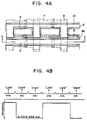
- Fig. 4A is a plan view of a charge-coupled device fabricated according to a second embodiment of the invention and Fig. 4B is a diagram showing a potential profile developed at a given time in the section taken along the line D - D in Fig. 4A.
- the diffusion front formed when the thermal process of the p+-type region 5 is completed stays within the p-type region 9a which is integrally formed with the gate region 9.
- the channel width of the channel transfer region is the same all the way through without the occurrence of a wide portion or a narrow portion.
- the mask pattern used for the formation of the p+-type region 5 has a pattern which takes into account in advance the lateral diffusion which develops during the thermal process in the p+-type region to become the element isolation region and which maintains a predetermined distance between the p+-type region and the n-type region to become the charge transfer region.
- the channel width of the charge transfer region is uniform which has made it possible to enhance the charge transfer efficiency due to the suppression of the occurrence of potential dips ⁇ ch which may be caused by narrow channel effects.
Landscapes
- Solid State Image Pick-Up Elements (AREA)
- Element Separation (AREA)
Applications Claiming Priority (2)
| Application Number | Priority Date | Filing Date | Title |
|---|---|---|---|
| JP93713/92 | 1992-03-19 | ||
| JP4093713A JP2910394B2 (ja) | 1992-03-19 | 1992-03-19 | 固体撮像素子およびその製造方法 |
Publications (2)
| Publication Number | Publication Date |
|---|---|
| EP0561418A2 true EP0561418A2 (de) | 1993-09-22 |
| EP0561418A3 EP0561418A3 (en) | 1994-04-27 |
Family
ID=14090069
Family Applications (1)
| Application Number | Title | Priority Date | Filing Date |
|---|---|---|---|
| EP19930104545 Withdrawn EP0561418A3 (en) | 1992-03-19 | 1993-03-19 | Method for fabricating charge-coupled device |
Country Status (3)
| Country | Link |
|---|---|
| US (1) | US5340766A (de) |
| EP (1) | EP0561418A3 (de) |
| JP (1) | JP2910394B2 (de) |
Cited By (1)
| Publication number | Priority date | Publication date | Assignee | Title |
|---|---|---|---|---|
| GB2319133A (en) * | 1996-11-07 | 1998-05-13 | Umax Data Systems Inc | Colour scanner using nonsquare CCD elements |
Families Citing this family (3)
| Publication number | Priority date | Publication date | Assignee | Title |
|---|---|---|---|---|
| EP0746034A3 (de) * | 1995-05-29 | 1998-04-29 | Matsushita Electronics Corporation | Festkörper-Bildaufnahmevorrichtung und Verfahren zur dessen Herstellung |
| JP4092409B2 (ja) * | 1999-08-18 | 2008-05-28 | 富士フイルム株式会社 | 固体撮像素子 |
| US7145122B2 (en) * | 2004-06-14 | 2006-12-05 | Omnivision Technologies, Inc. | Imaging sensor using asymmetric transfer transistor |
Family Cites Families (8)
| Publication number | Priority date | Publication date | Assignee | Title |
|---|---|---|---|---|
| JPS54114922A (en) * | 1978-02-27 | 1979-09-07 | Nec Corp | Two dimentional pick up element and its drive |
| US4216574A (en) * | 1978-06-29 | 1980-08-12 | Raytheon Company | Charge coupled device |
| US4276099A (en) * | 1978-10-11 | 1981-06-30 | The Secretary Of State For Defence In Her Britannic Majesty's Government Of The United Kingdom Of Great Britain And Northern Ireland | Fabrication of infra-red charge coupled devices |
| JPS5875382A (ja) * | 1981-07-20 | 1983-05-07 | Sony Corp | 固体撮像装置 |
| JPS6045057A (ja) * | 1983-08-23 | 1985-03-11 | Toshiba Corp | 固体撮像装置の製造方法 |
| US4683637A (en) * | 1986-02-07 | 1987-08-04 | Motorola, Inc. | Forming depthwise isolation by selective oxygen/nitrogen deep implant and reaction annealing |
| JPH02278874A (ja) * | 1989-04-20 | 1990-11-15 | Hitachi Ltd | 固体撮像素子及びその製造方法 |
| KR940009648B1 (ko) * | 1991-10-15 | 1994-10-15 | 금성일렉트론 주식회사 | 전하결합소자의 제조방법 |
-
1992
- 1992-03-19 JP JP4093713A patent/JP2910394B2/ja not_active Expired - Fee Related
-
1993
- 1993-03-17 US US08/032,147 patent/US5340766A/en not_active Expired - Lifetime
- 1993-03-19 EP EP19930104545 patent/EP0561418A3/en not_active Withdrawn
Cited By (1)
| Publication number | Priority date | Publication date | Assignee | Title |
|---|---|---|---|---|
| GB2319133A (en) * | 1996-11-07 | 1998-05-13 | Umax Data Systems Inc | Colour scanner using nonsquare CCD elements |
Also Published As
| Publication number | Publication date |
|---|---|
| US5340766A (en) | 1994-08-23 |
| JPH05267633A (ja) | 1993-10-15 |
| JP2910394B2 (ja) | 1999-06-23 |
| EP0561418A3 (en) | 1994-04-27 |
Similar Documents
| Publication | Publication Date | Title |
|---|---|---|
| US4844776A (en) | Method for making folded extended window field effect transistor | |
| US4845046A (en) | Process for producing semiconductor devices by self-alignment technology | |
| KR100260577B1 (ko) | 자기정렬형 콘택 형성방법 | |
| US4231051A (en) | Process for producing minimal geometry devices for VSLI applications utilizing self-aligned gates and self-aligned contacts, and resultant structures | |
| US4584761A (en) | Integrated circuit chip processing techniques and integrated chip produced thereby | |
| KR100218849B1 (ko) | 고체촬상소자의제조방법 | |
| US4686759A (en) | Method of manufacturing a semiconductor device | |
| US20070184653A1 (en) | Integrated circuit with a very small-sized reading diode | |
| EP0561418A2 (de) | Verfahren zur Herstellung einer Ladungverschiebanordnung | |
| US5447883A (en) | Method of manufacturing semiconductor device | |
| US4504333A (en) | Method of making field oxide regions | |
| JPH11330262A (ja) | 半導体装置の製造方法 | |
| US5627096A (en) | Manufacturing method of electric charge transferring devices | |
| JPS59181062A (ja) | Mos型半導体装置の製造方法 | |
| US4731318A (en) | Integrated circuit comprising MOS transistors having electrodes of metallic silicide and a method of fabrication of said circuit | |
| US3874915A (en) | Silicon nitride on silicon oxide coatings for semiconductor devices | |
| KR19990013587A (ko) | 고체 상태 화상 감지 장치 및 그 제조 방법 | |
| US5770464A (en) | Method for fabricating semiconductor devices having lightly doped drain | |
| JPS61176152A (ja) | ゲートと自己整合するコンタクト窓を有するダイオードの製造方法 | |
| KR100272558B1 (ko) | 고체 촬상 소자의 제조방법 | |
| KR100200697B1 (ko) | 가드링을 구비하는 반도체장치 및 이를 이용한 콘택트 형성방법 | |
| KR100218311B1 (ko) | 반도체장치의 소자격리구조 및 그 제조방법 | |
| KR950000853B1 (ko) | 반도체소자 제조방법 | |
| KR0123782B1 (ko) | Eprom반도체 장치 및 이의 형성방법 | |
| KR19990018373A (ko) | 랜딩 패드를 이용한 반도체소자의 콘택 형성방법 |
Legal Events
| Date | Code | Title | Description |
|---|---|---|---|
| PUAI | Public reference made under article 153(3) epc to a published international application that has entered the european phase |
Free format text: ORIGINAL CODE: 0009012 |
|
| AK | Designated contracting states |
Kind code of ref document: A2 Designated state(s): DE FR GB |
|
| PUAL | Search report despatched |
Free format text: ORIGINAL CODE: 0009013 |
|
| PUAF | Information related to the publication of a search report (a3 document) modified or deleted |
Free format text: ORIGINAL CODE: 0009199SEPU |
|
| PUAF | Information related to the publication of a search report (a3 document) modified or deleted |
Free format text: ORIGINAL CODE: 0009199SEPU |
|
| AK | Designated contracting states |
Kind code of ref document: A3 Designated state(s): DE FR GB |
|
| D17D | Deferred search report published (deleted) | ||
| D17D | Deferred search report published (deleted) | ||
| PUAL | Search report despatched |
Free format text: ORIGINAL CODE: 0009013 |
|
| AK | Designated contracting states |
Kind code of ref document: A3 Designated state(s): DE FR GB |
|
| 17P | Request for examination filed |
Effective date: 19940526 |
|
| 17Q | First examination report despatched |
Effective date: 19951107 |
|
| 18D | Application deemed to be withdrawn |
Effective date: 19960518 |