EP0568733B1 - Feuille de cuivre à bas profil et procédé pour fabriquer des feuilles métalliques aptes au laminage - Google Patents
Feuille de cuivre à bas profil et procédé pour fabriquer des feuilles métalliques aptes au laminage Download PDFInfo
- Publication number
- EP0568733B1 EP0568733B1 EP92121918A EP92121918A EP0568733B1 EP 0568733 B1 EP0568733 B1 EP 0568733B1 EP 92121918 A EP92121918 A EP 92121918A EP 92121918 A EP92121918 A EP 92121918A EP 0568733 B1 EP0568733 B1 EP 0568733B1
- Authority
- EP
- European Patent Office
- Prior art keywords
- foil
- electrolyte
- cathode
- copper
- electrodeposition
- Prior art date
- Legal status (The legal status is an assumption and is not a legal conclusion. Google has not performed a legal analysis and makes no representation as to the accuracy of the status listed.)
- Expired - Lifetime
Links
Images




Classifications
-
- C—CHEMISTRY; METALLURGY
- C25—ELECTROLYTIC OR ELECTROPHORETIC PROCESSES; APPARATUS THEREFOR
- C25D—PROCESSES FOR THE ELECTROLYTIC OR ELECTROPHORETIC PRODUCTION OF COATINGS; ELECTROFORMING; APPARATUS THEREFOR
- C25D1/00—Electroforming
- C25D1/04—Wires; Strips; Foils
-
- H—ELECTRICITY
- H05—ELECTRIC TECHNIQUES NOT OTHERWISE PROVIDED FOR
- H05K—PRINTED CIRCUITS; CASINGS OR CONSTRUCTIONAL DETAILS OF ELECTRIC APPARATUS; MANUFACTURE OF ASSEMBLAGES OF ELECTRICAL COMPONENTS
- H05K3/00—Apparatus or processes for manufacturing printed circuits
- H05K3/38—Improvement of the adhesion between the insulating substrate and the metal
- H05K3/382—Improvement of the adhesion between the insulating substrate and the metal by special treatment of the metal
- H05K3/384—Improvement of the adhesion between the insulating substrate and the metal by special treatment of the metal by plating
-
- H—ELECTRICITY
- H05—ELECTRIC TECHNIQUES NOT OTHERWISE PROVIDED FOR
- H05K—PRINTED CIRCUITS; CASINGS OR CONSTRUCTIONAL DETAILS OF ELECTRIC APPARATUS; MANUFACTURE OF ASSEMBLAGES OF ELECTRICAL COMPONENTS
- H05K2201/00—Indexing scheme relating to printed circuits covered by H05K1/00
- H05K2201/03—Conductive materials
- H05K2201/0332—Structure of the conductor
- H05K2201/0335—Layered conductors or foils
- H05K2201/0355—Metal foils
-
- H—ELECTRICITY
- H05—ELECTRIC TECHNIQUES NOT OTHERWISE PROVIDED FOR
- H05K—PRINTED CIRCUITS; CASINGS OR CONSTRUCTIONAL DETAILS OF ELECTRIC APPARATUS; MANUFACTURE OF ASSEMBLAGES OF ELECTRICAL COMPONENTS
- H05K2203/00—Indexing scheme relating to apparatus or processes for manufacturing printed circuits covered by H05K3/00
- H05K2203/03—Metal processing
- H05K2203/0307—Providing micro- or nanometer scale roughness on a metal surface, e.g. by plating of nodules or dendrites
-
- H—ELECTRICITY
- H05—ELECTRIC TECHNIQUES NOT OTHERWISE PROVIDED FOR
- H05K—PRINTED CIRCUITS; CASINGS OR CONSTRUCTIONAL DETAILS OF ELECTRIC APPARATUS; MANUFACTURE OF ASSEMBLAGES OF ELECTRICAL COMPONENTS
- H05K2203/00—Indexing scheme relating to apparatus or processes for manufacturing printed circuits covered by H05K3/00
- H05K2203/07—Treatments involving liquids, e.g. plating, rinsing
- H05K2203/0703—Plating
- H05K2203/0723—Electroplating, e.g. finish plating
-
- H—ELECTRICITY
- H05—ELECTRIC TECHNIQUES NOT OTHERWISE PROVIDED FOR
- H05K—PRINTED CIRCUITS; CASINGS OR CONSTRUCTIONAL DETAILS OF ELECTRIC APPARATUS; MANUFACTURE OF ASSEMBLAGES OF ELECTRICAL COMPONENTS
- H05K3/00—Apparatus or processes for manufacturing printed circuits
- H05K3/22—Secondary treatment of printed circuits
- H05K3/24—Reinforcing of the conductive pattern
- H05K3/241—Reinforcing of the conductive pattern characterised by the electroplating method; means therefor, e.g. baths or apparatus
Definitions
- This invention relates to an electrolytic process for producing metal foil according to claim 1, and to a copper foil produced accordingly and, more particularly, to a process for producing a copper foil for fabrication of printed circuit boards for electronic applications.
- the first step, fabrication of the base foil, or "core” is primarily responsible for imparting to the bulk of the foil the combination of physical, metallurgical and electrical properties desired in the printed circuit industry, and obviously, those properties are determined by the microstructure of the bulk of the foil, which in turn is determined by purity and conditions of the plating process.
- Typical properties of the core of the foil sought by printed circuit board manufacturers are suitable tensile strength, yield stress, elongation, ductility and resistance to fatigue. Many of properties relate to the maximum load the material may withstand before failure, and are usually derived from stress-strain curves.
- conductivity is considered an important property of copper foil. All these properties of copper foil depend on the foil's microstructure, but particularly on the microstructure of the core of the foil.
- an electrodeposit of metal e.g., copper
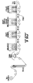
- the electrodeposited copper is continuously stripped from the rotating drum outer surface 23 (since the adhesion between copper electrodeposit and the drum surface is low) in the form of thin foil 34.
- a metal ion-containing electrolyte 33 is pumped into the gap 26 through one or more feed lines 33a from a dissolving tank 58, and the drum 21 is at least partially immersed in the electrolyte.
- the foil 34 at this stage has a matte side (the side facing the electrolyte) and a shiny side (the side facing the drum).
- foil 34 is rendered cathodic by means of contact rollers 37 and 38 and passes in a serpentine fashion through tanks 39 and 40, facing the rectangular anodes 41, 42, 43 and 44 as shown.
- Each tank has its own supply, respectively, of an appropriate barrier layer electrolyte and a stain-proofing electrolyte and its direct current power source(s) 45, 46 and 47. Between the tanks, the foil is thoroughly rinsed on both sides in baths 48 and 49.
- the matte side of the foil can be sprayed with a dilute solution (e.g., about 0.3% or 0.5%) of a primer or coupling agent (not shown).
- a dilute solution e.g., about 0.3% or 0.5%) of a primer or coupling agent (not shown).
- “Coupling agent” represents the best name and description a variety of chemically reactive bodies which are used in the glass-reinforced plastic industry. (See page 194, Adhesion And The Formulation Of Adhesives , William C. Wake, Elsevier Publishers).
- Refining agents used in electroplating are usually macro-molecular, water soluble colloids and polymers. Most popular are organic inhibitors such as gelatin, animal glue, cellulose ethers, polyacrylamide, and the like. They can be used separately, but mixtures are preferred, since mixtures can impart to electrodeposits properties impossible to obtain using a single inhibitor.
- a mixture of gelatin having a low molecular weight (less than 10,000), a higher molecular weight gelatin and a hydroxyalkyl cellulose such as hydroxyethyl cellulose has been found to be highly effective in obtaining a matte structure that is characterized by high bond and low profile height.
- FIG. 3 illustrates in greater detail the terminal portion 25a of primary exit anode 25 which is spaced apart and electrically insulated from secondary anode 27.
- the turbulent electrolyte flows upwardly in gap 26a, exits the first zone through a main solution exit 61 and is returned to the main body of electrolyte in tank 54.
- the solution leaving gap 26a at exit 61 takes with it the oxygen bubbles generated at the primary anode in the course of the electrodeposition of the core foil.
- the main solution exit 61 is a slot formed in an insulator block formed of a dielectric, e.g. an insulating resin such as polypropylene, which separates and electrically insulates anodes 25 and 27.
- the second zone ends and the bonding treatment is completed, with the combined height of the matte side and the treatment being about 7,6 ⁇ m (300 microinches) in the embodiment described herein.
- This product is referred to as low profile copper foil.
- the present invention also offers an advantage in terms of quality.
- the described drum-treatment due to its low-profile and the absence of breaking off, or transfer, of the nodules, or microprojections, is better than the traditional treatment.
- the region of depleted metal concentration does not extend very far from the cathode. Most of the concentration changes occur within a thin layer of solution adjacent to the cathode. It is called the cathode film or, more accurately, the diffusion, or boundary, layer. An understanding of the nature of this diffusion layer is of primary importance in applying diffusion theory to electroplating.
- Electrodeposits are "crystalline", i.e., are composed of "building units”, each of which is an arrangement of atoms repeated in three mutually perpendicular directions. Crystals which touch each other in a continuous fashion to make up metallic body are called grains. Grain size and orientation of electrodeposits vary widely causing variation of the deposit's "texture” or "morphology”, e.g., variation of the deposit's macroscopic and microscopic crystallographic characteristics.
- crystal growth consists first of the formation of nuclei or minute new crystals followed by the growth of existing crystals. Any "plating condition" that increases the rate of formation of nuclei tend to increase the number of crystals, while the opposing conditions inhibit the increase.
- the diffusion layer is very thin and the difference between copper concentration in the bulk of the electrolyte and the liquid-solid interface, is quite low.
- Copper plated under such conditions and in addition in the presence of refining agents has a micro-structure that consists of finegrained and densely packed, base-oriented crystallites. As a result of such micro-structure the core of the foil is endowed with excellent mechanical and metallurgical properties, indispensable in printed circuit industry.
- the outer surface of the 'core' is composed of dense, conical, micro-peaks and micro-valleys.
- the electrolyte is the same as in the first zone, the other conditions that determine mass-transfer are deliberately arranged and maintained as to have a poor mass transfer. Accordingly, such conditions encourage electrodeposition of field-oriented micro-structures deposited densely over the micro-peaks of the surface of 'core' deposit formed in the preceding (first) electrodeposition zone.
- Field-oriented growth habit is a result of poor mass transfer and attendant high concentration polarization. These conditions, in turn, are the result of high current density and laminar flow of the electrolyte (i.e., condition of natural convection, as opposed to forced convection in the first electrodeposition zone). Consequently, the diffusion layer is thick and the difference between copper concentration in the bulk of the electrolyte and the liquid-solid interface is high, while the J/Jdl ratio is low. Under such conditions, and in addition in the presence of refining agents the copper electrodeposit consists of dense, spherical micro-projections, distributed densely over the micro-peaks of the surface of the 'core' deposit formed in the preceding (first) electrodeposition zone.
- This coating of spherical micro-projections constitutes a 'bonding treatment' on the matte side of the foil, since it greatly enhances surface area available for bonding to the polymeric materials.
- the second electrodeposition zone produces on the matte side of the foil a deposit characterized by a roughness factor (a ratio of the true area to the apparent area) that is best for bonding copper foil to the polymeric substrates.
- the present invention also takes advantage of anomalous behavior of refining agents in respect to the influence these agents have on the microstructure and therefore on the properties and functional applications of electrodeposits.
- Refining agents in combination with excellent mass transfer conditions (as represented by J/Jdl ratio) in the first electrodeposition zone diminish the grain size of the deposit and thus help to produce base oriented, fine grained and compact electrodeposit -- in short, a structure which assures that the properties and functions of the 'core' of the foil (formed in first electrodeposition zone) are very good.
- refining agents combined with poor mass transfer conditions, as in the second electrodeposition zone help to produce field oriented micronodular deposits whose individual particles project outward from the surface of the foil and are micro-spherical in shape. Such spherical microdeposits function excellently as a 'bonding treatment' between copper foil and polymeric substrates.
- the electrocrystallization (crystal habit) of electrodeposited metal is affected by the mass transfer of the metal ions to the cathode.
- this mass transfer can be characterized by the ratio of the current density and the bulk concentration of the metal ions (C).
- the ratio of current density and the limiting current density also called diffusion limiting current density, Jdl
- J Jdl diffusion limiting current density
- a shift from one type of electrodeposit's structure to another type of structure can be achieved by shifting the J/Jdl ratio, or the J/C ratio.
- inhibitors sometimes called refining agents
- refining agents The role of inhibitors, sometimes called refining agents, is perhaps one of the most important factors that influences electrodeposition and treatment process.
- Temperature is extremely important in the mass transfer since it influences diffusion dramatically. However, temperature influences mass transfer in a manner similar to the copper concentration. Increased temperature changes the microstructure of the deposit somewhat similarly to the increase in Cu concentration; the reverse is also true. It is advantageous to keep the temperature constant, most preferably at about 65°C, although the temperature selected may vary in accordance with other process parameters.
- the electrolyte velocity is instrumental in achieving uniform and low profile, high bond micro-structures. Turbulent flow thins down the diffusion layer and thus moves the limiting current density to much higher values.
- the drum-treater apparatus of the present invention should be equipped with pumps capable of generating an electrolyte velocity in the first zone of up to 3 m/sec. Moving to higher velocity values improves the chances of accommodating, at the same time, criteria of high peel-strength and the uniformity of Rz and appearance of the copper foil.
- gelatin An extremely low concentration of gelatin greatly influences the structure and thus, the properties of the foil. It appears that one molecule of gelatin may and does influence a very large number of copper ions. There is little doubt that adsorption of the gelatin is essential to its mode of moderating the copper deposition process and the formation of the bonding surface. Since the gelatin molecules in our electrolyte are charged positively, it is likely that gelatin is subject to electrosorption at the cathode. Adsorption of gelatin tends to reduce the size of the crystals in the deposit. It may be that gelatin behaves as an inhibitor of deposition (on local scale), decreasing the local deposition rate and increasing polarization. Such effects enhance formation of new crystal nuclei on the metal surface and suppress growth of existing crystallites, thus resulting in a finer crystal structure. It follows, then, that on a micro-scale gelatin has a leveling effect on copper deposits.
- the boundary of the diffusion layer does not follow the profile contour of the cathode (matte side of the growing foil), but lies farther from the depth of the valleys than from the peaks.
- the effective thickness of diffusion layer shows, therefore, variations which result in variations of local concentration polarization. Since the potential of the cathode is uniform, differences in the local rate of metal deposition will depend on the diffusion rate of copper ions and molecules of gelatin.
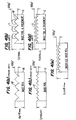
- FIG. 5 shows the active deposition phenomenon at an operating cathode (matte side of the foil 34 in electrolyte bath 33) with gelatin 71 accumulated at peaks 34a because the diffusion rate is relatively rapid over the short distance from the diffusion layer boundary, while at valleys 34b diffusion is too slow to keep up with consumption of gelatin. Copper deposition is relatively inhibited at the peaks but not in the valleys, and thus a smoother surface results.
- a 0,3 kg/m 2 (1 oz.) copper foil was made in accordance with the present invention on a plating machine of the type described above and as illustrated in Figs. 1 and 3 employing the most preferred plating parameters, refining agents and electrolyte described above.
- the foil was stain proofed by electrodepositing a chromate layer, followed by spray application of glycidoxy silane on the matte surface of the foil.
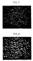
- Fig. 7 is a photomicrograph (1000x), taken at an incident angle of 45°, showing the matte surface of the resulting foil.
- the resulting foil was then laminated to an epoxy/glass fiber prepreg, and the peel strength was measured and found to be (11 lbs/in) 19,3 ⁇ 10 2 N/m.
Landscapes
- Engineering & Computer Science (AREA)
- Chemical & Material Sciences (AREA)
- Chemical Kinetics & Catalysis (AREA)
- Electrochemistry (AREA)
- Materials Engineering (AREA)
- Metallurgy (AREA)
- Organic Chemistry (AREA)
- Manufacturing & Machinery (AREA)
- Microelectronics & Electronic Packaging (AREA)
- Electroplating Methods And Accessories (AREA)
- Electrolytic Production Of Metals (AREA)
- Parts Printed On Printed Circuit Boards (AREA)
Claims (5)
- Procédé électrolytique pour produire une feuille métallique ayant une surface traitée à profil bas, lequel procédé comprend des phases consistant :(a) à faire passer un courant électrique dans une solution d'électrolyte, ledit électrolyte contenant une concentration d'ions métalliques et un agent d'affinage des grains se composant d'un mélange au moins d'une gélatine et d'un éther cellulosique, d'une anode principale à une cathode espacée de ladite anode dans une première zone d'électrodéposition ayant une première densité de courant comprise entre 20 A/DCM2 environ et 100 A/DCM2 environ, tout en faisant circuler ledit électrolyte entre ladite cathode et ladite anode principale dans des conditions d'écoulement turbulent ayant une vitesse d'au moins 0,8 m/s pour déposer par électrolyse, sur ladite cathode, une feuille principale de métal ayant une surface mate ; et(b) à faire passer un courant électrique dans ladite solution d'électrolyte, depuis une anode secondaire isolée électriquement de ladite anode principale et espacée de ladite cathode jusqu'à ladite cathode dans une seconde zone d'électrodéposition ayant une seconde densité de courant qui est supérieure à celle dans ladite première zone d'électrodéposition et qui est au moins de 100 A/DCM2 environ mais non supérieure à la densité de courant limite, tout en faisant circuler l'électrolyte dans ladite seconde zone entre ladite cathode et ladite anode secondaire dans des conditions d'écoulement laminaire ayant une vitesse d'environ 0,1 m/s ou moins pour déposer par électrolyse des micro-nodules dudit métal sur ladite surface mate.
- Procédé selon la revendication 1, dans lequel ledit électrolyte dans ladite seconde zone d'électrodéposition contient un mélange de gélatines ayant différents poids moléculaires et d'hydroxyalkylcellulose.
- Procédé selon la revendication 1, dans lequel(a) ladite cathode est une cathode de tambour rotatif au moins immergée partiellement dans ledit électrolyte ; et(b) l'électrolyte, circulé dans chacune desdites première et seconde zones d'électrodéposition, comprend une solution de sulfate de cuivre et d'acide sulfurique ayant une concentration en cuivre comprise entre 30 g/l et 100 g/l, une concentration en acide sulfurique comprise entre 40 g/l et 150 g/l, contient un agent d'affinage des grains de gélatine/éther cellulosique, et est maintenu à une température comprise entre 38°C et 82°C (entre 100°F et 180°F).
- Feuille de cuivre produite par le procédé selon la revendication 1.
- Feuille de cuivre produite par le procédé selon la revendication 3.
Applications Claiming Priority (2)
| Application Number | Priority Date | Filing Date | Title |
|---|---|---|---|
| US878973 | 1992-05-06 | ||
| US07/878,973 US5215646A (en) | 1992-05-06 | 1992-05-06 | Low profile copper foil and process and apparatus for making bondable metal foils |
Publications (3)
| Publication Number | Publication Date |
|---|---|
| EP0568733A2 EP0568733A2 (fr) | 1993-11-10 |
| EP0568733A3 EP0568733A3 (en) | 1994-05-11 |
| EP0568733B1 true EP0568733B1 (fr) | 1997-11-12 |
Family
ID=25373190
Family Applications (1)
| Application Number | Title | Priority Date | Filing Date |
|---|---|---|---|
| EP92121918A Expired - Lifetime EP0568733B1 (fr) | 1992-05-06 | 1992-12-23 | Feuille de cuivre à bas profil et procédé pour fabriquer des feuilles métalliques aptes au laminage |
Country Status (4)
| Country | Link |
|---|---|
| US (1) | US5215646A (fr) |
| EP (1) | EP0568733B1 (fr) |
| JP (1) | JPH0681186A (fr) |
| DE (1) | DE69223135T2 (fr) |
Cited By (1)
| Publication number | Priority date | Publication date | Assignee | Title |
|---|---|---|---|---|
| WO2023117126A1 (fr) * | 2021-12-24 | 2023-06-29 | Circuit Foil Luxembourg | Feuille de cuivre électrolytique à double couche et son procédé de fabrication |
Families Citing this family (41)
| Publication number | Priority date | Publication date | Assignee | Title |
|---|---|---|---|---|
| US5431803A (en) | 1990-05-30 | 1995-07-11 | Gould Electronics Inc. | Electrodeposited copper foil and process for making same |
| US5447619A (en) * | 1993-11-24 | 1995-09-05 | Circuit Foil Usa, Inc. | Copper foil for the manufacture of printed circuit boards and method of producing the same |
| US5509557A (en) * | 1994-01-24 | 1996-04-23 | International Business Machines Corporation | Depositing a conductive metal onto a substrate |
| AUPM694694A0 (en) * | 1994-07-21 | 1994-08-11 | M.I.M. Holdings Limited | Prevention of cathode corrosion during electrowinning |
| US6344131B1 (en) * | 1994-08-30 | 2002-02-05 | Fuji Photo Film Co., Ltd. | Method of producing aluminum support for planographic printing plate |
| JP3587574B2 (ja) * | 1994-11-30 | 2004-11-10 | 株式会社日立グローバルストレージテクノロジーズ | 磁気ディスク装置 |
| JP3155920B2 (ja) * | 1996-01-16 | 2001-04-16 | 三井金属鉱業株式会社 | プリント配線板用電解銅箔及びその製造方法 |
| JP3388693B2 (ja) * | 1996-12-04 | 2003-03-24 | 日本ステンレス工材株式会社 | 電着ドラム |
| JPH10330983A (ja) * | 1997-05-30 | 1998-12-15 | Fukuda Metal Foil & Powder Co Ltd | 電解銅箔及びその製造方法 |
| US5863410A (en) * | 1997-06-23 | 1999-01-26 | Circuit Foil Usa, Inc. | Process for the manufacture of high quality very low profile copper foil and copper foil produced thereby |
| US6270645B1 (en) | 1997-09-26 | 2001-08-07 | Circuit Foil Usa, Inc. | Simplified process for production of roughened copper foil |
| JP3784528B2 (ja) * | 1998-03-05 | 2006-06-14 | 三菱伸銅株式会社 | 表面処理金属材料およびその製造方法 |
| DE19857157A1 (de) * | 1998-12-11 | 2000-06-15 | Bolta Werke Gmbh | Verfahren zur Herstellung einer selbsttragenden Metallfolie |
| US6183607B1 (en) * | 1999-06-22 | 2001-02-06 | Ga-Tek Inc. | Anode structure for manufacture of metallic foil |
| JP3458781B2 (ja) * | 1999-07-06 | 2003-10-20 | ダイソー株式会社 | 金属箔の製造方法 |
| DE60042976D1 (de) * | 1999-08-06 | 2009-10-29 | Ibiden Co Ltd | Lösung für die elektrochemische abscheidung, methode, eine leiterplatte unter verwendung dieser lösung herzustellen und mehrschichtige leiterplatte |
| DE19937843C1 (de) * | 1999-08-13 | 2001-02-08 | Bolta Werke Gmbh | Verfahren zur Herstellung einer selbsttragenden Kupferfolie |
| US6270648B1 (en) | 1999-10-22 | 2001-08-07 | Yates Foil Usa, Inc. | Process and apparatus for the manufacture of high peel-strength copper foil useful in the manufacture of printed circuit boards, and laminates made with such foil |
| DE10037521C2 (de) * | 1999-11-18 | 2002-04-25 | Saxon Screens Rotationsschablo | Verfahren zur elektrolytischen Herstellung von Rotationssiebdruckformen |
| JP3670186B2 (ja) * | 2000-01-28 | 2005-07-13 | 三井金属鉱業株式会社 | プリント配線板用表面処理銅箔の製造方法 |
| JP3670185B2 (ja) * | 2000-01-28 | 2005-07-13 | 三井金属鉱業株式会社 | プリント配線板用表面処理銅箔の製造方法 |
| JP2001284797A (ja) * | 2000-03-28 | 2001-10-12 | Kyocera Corp | 多層配線基板及びその製造方法 |
| US6361673B1 (en) | 2000-06-27 | 2002-03-26 | Ga-Tek Inc. | Electroforming cell |
| KR100454270B1 (ko) * | 2002-11-29 | 2004-10-26 | 엘지전선 주식회사 | 저조도 전해동박의 제조방법 및 전해동박 |
| TW200424359A (en) | 2003-02-04 | 2004-11-16 | Furukawa Circuit Foil | Copper foil for high frequency circuit, method of production and apparatus for production of same, and high frequency circuit using copper foil |
| KR100694382B1 (ko) * | 2005-05-02 | 2007-03-12 | 엘에스전선 주식회사 | 고강도를 갖는 저조도 전해동박의 제조방법, 이 방법에의해 제조된 전해동박, 및 이 전해동박을 사용하여 제작한전자 부품 |
| TW200738913A (en) * | 2006-03-10 | 2007-10-16 | Mitsui Mining & Smelting Co | Surface treated elctrolytic copper foil and process for producing the same |
| KR100730834B1 (ko) * | 2006-03-15 | 2007-06-20 | 엘에스전선 주식회사 | 전해 동박 제조용 드럼의 버핑장치 및 버핑방법 |
| KR101390507B1 (ko) * | 2011-08-30 | 2014-04-30 | 니시 코교 가부시키가이샤 | 천공박 전해 석출 장치 |
| KR102136784B1 (ko) * | 2015-07-24 | 2020-07-22 | 케이씨에프테크놀로지스 주식회사 | 리튬 이차전지용 전해동박 및 이를 포함하는 리튬 이차전지 |
| KR102029139B1 (ko) * | 2015-11-09 | 2019-10-07 | 케이씨에프테크놀로지스 주식회사 | 전해동박, 그것을 포함하는 전극, 그것을 포함하는 이차전지, 및 그것의 제조방법 |
| US9673646B1 (en) * | 2016-08-19 | 2017-06-06 | Chang Chun Petrochemical Co., Ltd. | Surface-treated electrolytic copper foil and method for wireless charging of flexible printed circuit board |
| CN108425135B (zh) * | 2017-02-15 | 2020-02-07 | 金居开发股份有限公司 | 电解铜箔的生产设备及其电流调整控制装置 |
| KR200494838Y1 (ko) * | 2017-09-11 | 2022-01-06 | 에스케이넥실리스 주식회사 | 전해동박 제조장치 |
| DE102020107907B4 (de) | 2020-03-23 | 2023-10-26 | Jacob Zimmermann | Vorrichtung zur elektrochemischen Herstellung dünner Folien und Verfahren zur elektrochemischen Herstellung dünner Folien |
| CN113699571B (zh) * | 2021-10-29 | 2022-01-18 | 苏州睿锂物联科技有限公司 | 一种可提高材料性能的锂电池铜箔表面预处理装置 |
| CN114032586A (zh) * | 2021-11-11 | 2022-02-11 | 浙江花园新能源股份有限公司 | 一种提升电解铜箔m面颗粒均匀性的电解液、生产工艺及产品 |
| CN114045536B (zh) * | 2021-12-13 | 2023-05-23 | 南开大学 | 一种兼具高强度和高延性的梯度超薄铜箔制备方法 |
| CN114438574A (zh) * | 2022-03-21 | 2022-05-06 | 中山大学 | 一种梯度结构多孔表面的电沉积制备装置和方法 |
| CN116497427A (zh) * | 2023-05-16 | 2023-07-28 | 广东嘉元科技股份有限公司 | 一种铜箔电镀试验装置 |
| CN120575302B (zh) * | 2025-08-04 | 2025-12-16 | 蓝帆新材料技术(广州)有限公司 | 电解铜箔及其制备方法、复合铜箔及集流体 |
Family Cites Families (9)
| Publication number | Priority date | Publication date | Assignee | Title |
|---|---|---|---|---|
| US3625844A (en) * | 1969-06-05 | 1971-12-07 | Circult Foll Corp | Stainproofing process and products resulting therefrom |
| US3674656A (en) * | 1969-06-19 | 1972-07-04 | Circuit Foil Corp | Bonding treatment and products produced thereby |
| SU461655A1 (ru) * | 1970-07-07 | 1976-05-05 | Государственный научно-исследовательский институт цветных металлов | Способ электролитического получени медной фольги |
| US3857681A (en) * | 1971-08-03 | 1974-12-31 | Yates Industries | Copper foil treatment and products produced therefrom |
| GB1373577A (en) * | 1972-05-10 | 1974-11-13 | Gnii Tsvetnykh Metallov | Electrolytic production of metal bands |
| US3853716A (en) * | 1972-09-08 | 1974-12-10 | Yates Industries | Electrolytic copper stainproofing process |
| US4572768A (en) * | 1985-06-28 | 1986-02-25 | Square D Company | Treatment for copper foil |
| FI873643A0 (fi) * | 1985-12-24 | 1987-08-24 | Gould Inc | Foerfarande och anlaeggning foer galvanisering av kopparfilm. |
| EP0442187B1 (fr) * | 1990-02-16 | 1994-02-02 | Furukawa Circuit Foil Co., Ltd. | Procédé de fabrication d'une feuille de cuivre par électrodéposition |
-
1992
- 1992-05-06 US US07/878,973 patent/US5215646A/en not_active Expired - Lifetime
- 1992-12-21 JP JP4340767A patent/JPH0681186A/ja active Pending
- 1992-12-23 DE DE69223135T patent/DE69223135T2/de not_active Expired - Fee Related
- 1992-12-23 EP EP92121918A patent/EP0568733B1/fr not_active Expired - Lifetime
Cited By (2)
| Publication number | Priority date | Publication date | Assignee | Title |
|---|---|---|---|---|
| WO2023117126A1 (fr) * | 2021-12-24 | 2023-06-29 | Circuit Foil Luxembourg | Feuille de cuivre électrolytique à double couche et son procédé de fabrication |
| EP4202084A3 (fr) * | 2021-12-24 | 2023-10-04 | Circuit Foil Luxembourg | Feuille de cuivre électrolytique à double couche et son procédé de fabrication |
Also Published As
| Publication number | Publication date |
|---|---|
| US5215646A (en) | 1993-06-01 |
| DE69223135D1 (de) | 1997-12-18 |
| EP0568733A2 (fr) | 1993-11-10 |
| EP0568733A3 (en) | 1994-05-11 |
| DE69223135T2 (de) | 1998-03-05 |
| JPH0681186A (ja) | 1994-03-22 |
Similar Documents
| Publication | Publication Date | Title |
|---|---|---|
| US5215646A (en) | Low profile copper foil and process and apparatus for making bondable metal foils | |
| US5863410A (en) | Process for the manufacture of high quality very low profile copper foil and copper foil produced thereby | |
| AU640169B2 (en) | Electrodeposited foil with controlled properties for printed circuit board applications and procedures and electrolyte bath solutions for preparing the same | |
| US4898647A (en) | Process and apparatus for electroplating copper foil | |
| CA2233329C (fr) | Procede de depot de couches metalliques par voie electrolytique | |
| KR100407732B1 (ko) | 결절상구리/니켈합금피막을포함하는복합호일,이를포함하는인쇄회로기판및결절상구리/니켈합금피막의전착방법 | |
| JP3281783B2 (ja) | プリント配線板用銅箔、その製造法及び電解装置 | |
| WO2007082112A2 (fr) | Procédé d'électrodéposition d'étain et d'alliage d'étain avec contrainte interne et granulométrie commandées de la déposition obtenue | |
| US3769179A (en) | Copper plating process for printed circuits | |
| CN114574911A (zh) | 一种高厚径比线路板通孔电镀工艺 | |
| EP0250195A2 (fr) | Feuille de cuivre ayant un fini mat des deux côtés | |
| JPH0424439B2 (fr) | ||
| US6270648B1 (en) | Process and apparatus for the manufacture of high peel-strength copper foil useful in the manufacture of printed circuit boards, and laminates made with such foil | |
| TWI683931B (zh) | 電解鍍銅用陽極及使用其之電解鍍銅裝置 | |
| JPS5867886A (ja) | 濃度勾配を有する鉄一亜鉛合金めつき層で被覆された鋼材およびその製造方法 | |
| Lee et al. | Evaluating and monitoring nucleation and growth in copper foil | |
| EP0181430A1 (fr) | Systèmes pour la fabrication d'une feuille métallique électroplaquée et/ou traitée | |
| JPH05140795A (ja) | 金属板に支持された電解銅箔の製造方法 | |
| JPS6324088A (ja) | 電着銅箔及びその製造方法 | |
| JP2629018B2 (ja) | 粗化めっき方法 | |
| Amadi | Agitation for the electrodeposition of printed circuit boards | |
| KR20210131832A (ko) | 합금도금층을 포함한 금속판 제조 방법 | |
| JPS62177193A (ja) | パラジウム・ニツケル合金メツキ液及びメツキ法 | |
| CN104718319A (zh) | 具有合金镀层的金属板的制造方法 | |
| EP1354077B1 (fr) | Dispositif et procede pour le depot en continu d'une couche contenant du nickel sur une feuille metallique |
Legal Events
| Date | Code | Title | Description |
|---|---|---|---|
| PUAI | Public reference made under article 153(3) epc to a published international application that has entered the european phase |
Free format text: ORIGINAL CODE: 0009012 |
|
| AK | Designated contracting states |
Kind code of ref document: A2 Designated state(s): BE DE FR GB IT LU NL SE |
|
| PUAL | Search report despatched |
Free format text: ORIGINAL CODE: 0009013 |
|
| AK | Designated contracting states |
Kind code of ref document: A3 Designated state(s): BE DE FR GB IT LU NL SE |
|
| 17P | Request for examination filed |
Effective date: 19941109 |
|
| 17Q | First examination report despatched |
Effective date: 19950428 |
|
| GRAG | Despatch of communication of intention to grant |
Free format text: ORIGINAL CODE: EPIDOS AGRA |
|
| GRAH | Despatch of communication of intention to grant a patent |
Free format text: ORIGINAL CODE: EPIDOS IGRA |
|
| GRAH | Despatch of communication of intention to grant a patent |
Free format text: ORIGINAL CODE: EPIDOS IGRA |
|
| GRAA | (expected) grant |
Free format text: ORIGINAL CODE: 0009210 |
|
| AK | Designated contracting states |
Kind code of ref document: B1 Designated state(s): BE DE FR GB IT LU NL SE |
|
| REF | Corresponds to: |
Ref document number: 69223135 Country of ref document: DE Date of ref document: 19971218 |
|
| ITF | It: translation for a ep patent filed | ||
| ET | Fr: translation filed | ||
| PLBE | No opposition filed within time limit |
Free format text: ORIGINAL CODE: 0009261 |
|
| STAA | Information on the status of an ep patent application or granted ep patent |
Free format text: STATUS: NO OPPOSITION FILED WITHIN TIME LIMIT |
|
| 26N | No opposition filed | ||
| REG | Reference to a national code |
Ref country code: GB Ref legal event code: IF02 |
|
| PGFP | Annual fee paid to national office [announced via postgrant information from national office to epo] |
Ref country code: FR Payment date: 20021127 Year of fee payment: 11 |
|
| PGFP | Annual fee paid to national office [announced via postgrant information from national office to epo] |
Ref country code: NL Payment date: 20021128 Year of fee payment: 11 |
|
| PGFP | Annual fee paid to national office [announced via postgrant information from national office to epo] |
Ref country code: SE Payment date: 20021129 Year of fee payment: 11 |
|
| PGFP | Annual fee paid to national office [announced via postgrant information from national office to epo] |
Ref country code: LU Payment date: 20021216 Year of fee payment: 11 |
|
| PGFP | Annual fee paid to national office [announced via postgrant information from national office to epo] |
Ref country code: GB Payment date: 20021218 Year of fee payment: 11 |
|
| PGFP | Annual fee paid to national office [announced via postgrant information from national office to epo] |
Ref country code: DE Payment date: 20021230 Year of fee payment: 11 |
|
| PGFP | Annual fee paid to national office [announced via postgrant information from national office to epo] |
Ref country code: BE Payment date: 20030108 Year of fee payment: 11 |
|
| PG25 | Lapsed in a contracting state [announced via postgrant information from national office to epo] |
Ref country code: LU Free format text: LAPSE BECAUSE OF NON-PAYMENT OF DUE FEES Effective date: 20031223 Ref country code: GB Free format text: LAPSE BECAUSE OF NON-PAYMENT OF DUE FEES Effective date: 20031223 |
|
| PG25 | Lapsed in a contracting state [announced via postgrant information from national office to epo] |
Ref country code: SE Free format text: LAPSE BECAUSE OF NON-PAYMENT OF DUE FEES Effective date: 20031224 |
|
| PG25 | Lapsed in a contracting state [announced via postgrant information from national office to epo] |
Ref country code: BE Free format text: LAPSE BECAUSE OF NON-PAYMENT OF DUE FEES Effective date: 20031231 |
|
| BERE | Be: lapsed |
Owner name: *CIRCUIT FOIL U.S.A. INC. Effective date: 20031231 |
|
| PG25 | Lapsed in a contracting state [announced via postgrant information from national office to epo] |
Ref country code: NL Free format text: LAPSE BECAUSE OF NON-PAYMENT OF DUE FEES Effective date: 20040701 Ref country code: DE Free format text: LAPSE BECAUSE OF NON-PAYMENT OF DUE FEES Effective date: 20040701 |
|
| EUG | Se: european patent has lapsed | ||
| GBPC | Gb: european patent ceased through non-payment of renewal fee |
Effective date: 20031223 |
|
| PG25 | Lapsed in a contracting state [announced via postgrant information from national office to epo] |
Ref country code: FR Free format text: LAPSE BECAUSE OF NON-PAYMENT OF DUE FEES Effective date: 20040831 |
|
| NLV4 | Nl: lapsed or anulled due to non-payment of the annual fee |
Effective date: 20040701 |
|
| REG | Reference to a national code |
Ref country code: FR Ref legal event code: ST |
|
| PG25 | Lapsed in a contracting state [announced via postgrant information from national office to epo] |
Ref country code: IT Free format text: LAPSE BECAUSE OF NON-PAYMENT OF DUE FEES;WARNING: LAPSES OF ITALIAN PATENTS WITH EFFECTIVE DATE BEFORE 2007 MAY HAVE OCCURRED AT ANY TIME BEFORE 2007. THE CORRECT EFFECTIVE DATE MAY BE DIFFERENT FROM THE ONE RECORDED. Effective date: 20051223 |