EP0569858A2 - Dispositif de mémoire - Google Patents
Dispositif de mémoire Download PDFInfo
- Publication number
- EP0569858A2 EP0569858A2 EP93107377A EP93107377A EP0569858A2 EP 0569858 A2 EP0569858 A2 EP 0569858A2 EP 93107377 A EP93107377 A EP 93107377A EP 93107377 A EP93107377 A EP 93107377A EP 0569858 A2 EP0569858 A2 EP 0569858A2
- Authority
- EP
- European Patent Office
- Prior art keywords
- data
- address
- memory device
- memory
- ccd array
- Prior art date
- Legal status (The legal status is an assumption and is not a legal conclusion. Google has not performed a legal analysis and makes no representation as to the accuracy of the status listed.)
- Ceased
Links
Images


Classifications
-
- G—PHYSICS
- G11—INFORMATION STORAGE
- G11C—STATIC STORES
- G11C7/00—Arrangements for writing information into, or reading information out from, a digital store
- G11C7/22—Read-write [R-W] timing or clocking circuits; Read-write [R-W] control signal generators or management
-
- G—PHYSICS
- G11—INFORMATION STORAGE
- G11C—STATIC STORES
- G11C11/00—Digital stores characterised by the use of particular electric or magnetic storage elements; Storage elements therefor
- G11C11/56—Digital stores characterised by the use of particular electric or magnetic storage elements; Storage elements therefor using storage elements with more than two stable states represented by steps, e.g. of voltage, current, phase, frequency
- G11C11/5621—Digital stores characterised by the use of particular electric or magnetic storage elements; Storage elements therefor using storage elements with more than two stable states represented by steps, e.g. of voltage, current, phase, frequency using charge storage in a floating gate
-
- G—PHYSICS
- G11—INFORMATION STORAGE
- G11C—STATIC STORES
- G11C27/00—Electric analogue stores, e.g. for storing instantaneous values
- G11C27/04—Shift registers
-
- G—PHYSICS
- G11—INFORMATION STORAGE
- G11C—STATIC STORES
- G11C8/00—Arrangements for selecting an address in a digital store
- G11C8/06—Address interface arrangements, e.g. address buffers
-
- G—PHYSICS
- G11—INFORMATION STORAGE
- G11C—STATIC STORES
- G11C11/00—Digital stores characterised by the use of particular electric or magnetic storage elements; Storage elements therefor
- G11C11/56—Digital stores characterised by the use of particular electric or magnetic storage elements; Storage elements therefor using storage elements with more than two stable states represented by steps, e.g. of voltage, current, phase, frequency
-
- G—PHYSICS
- G11—INFORMATION STORAGE
- G11C—STATIC STORES
- G11C2211/00—Indexing scheme relating to digital stores characterized by the use of particular electric or magnetic storage elements; Storage elements therefor
- G11C2211/56—Indexing scheme relating to G11C11/56 and sub-groups for features not covered by these groups
- G11C2211/564—Miscellaneous aspects
- G11C2211/5644—Multilevel memory comprising counting devices
-
- G—PHYSICS
- G11—INFORMATION STORAGE
- G11C—STATIC STORES
- G11C27/00—Electric analogue stores, e.g. for storing instantaneous values
Definitions
- the present invention relates to a memory device, especially to that effective for storing analog data or multilevel data.
- the present invention solves the above-mentioned problems and has an object to provide a memory device for realizing an analog memory or a multilevel memory easy to produce and of small scale circuit.
- a memory device realizes the small scale cell by means of storing analog data by circulating data on a plural number of linear CCD arrays, makes it possible to access in high speed by reading and writing data through cache memory, and by registering on an address register the address of the data in cache memory.
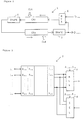
- Figure 1 shows a block diagram of an embodiment of a memory device according to the present invention.
- Figure 2 shows a block diagram of a loop array of a CCD of the embodiment in Figure 1.
- Figure 3 shows a block diagram of a cache memory of the embodiment in Figure 1.
- Figure 4 shows an image of an address register of the embodiment in Figure 1.
- Figure 1 shows the whole circuit of the memory device. Main memory 1 and cache memory 2 are comprised in it.
- main memory 1 a plural number of looped CCD array "L” are connected in parallel.
- the CCD array is connected CCD array CAa by looping.
- the groups of CCD array CAa and CAb are expressed by CAa' and CAb', respectively, in Figure 1.
- CCD array CAa transmits data to the end direction in keeping it, and CCD array CAb returns data to the start point in keeping it. Therefore, the CCD array keeps data in the whole of the circular root and has the capacity for twice scale of data than that for storing data in one way. It is also possible to simplify the circuit by forming the return root by simple conductor.
- CCD array CAa and CAb connects shaping circuits 3 and 4, respectively, on their ends. Deteriorated data is restored by A/D converting function of these shaping circuits.
- the output of shaping circuit 3 is connected to CCD array CAb through multiplexer 5 for 2 inputs and new data can be written from Din.
- Branch Dout is set on the output of shaping circuit 3.
- Data can be read from the branch Dout. It is shown in Figure 1 by "DATA".
- DATA Generally, a CCD has more simpler structure than a cell of an usual DRAM. The necessary area for the storage of 1 datum is small and analog data can be stored in a cell. Therefore it is possible to realize a memory with more larger capacity than that of general DRAM.
- Cache memory 2 is a high speed RAM for once storing data to read and write from/in main memory 1 (SRAM is usually used). It comprises row address from L1 to Ln of the numbers corresponding to each CCD array loop "L". It means that a unit of data of all array loops can be simultaneously transmitted from main memory 1 to cache memory 2, and vice versa. High speed of transmission is guaranteed by it.
- the data of CCD array is transmitted by CLK and circulates on the loop array.
- a fixed address is commonly defined to all array loops.
- the address of the data on the end point of array CAa is given by address counter 6.
- the address of a CCD array is always controlled by address counter.
- a dummy CCD array loop is set in the main memory (shown by "DUMMY” in Figure 1) and the address of the main memory is registered on the array.
- the addresses of multiplexer 7 and selector 8 are designated by inputting upper bits from A23 to A13 of ADR from outside of the device. As these upper bits address are simultaneously input to address register 9, the address of the data stored in the cache memory can be identified by checking the content in the address register. The check is executed by comparator 10 which is set by the same number of the addresses to be stored ("k", in Figures 3 and 4).
- the lower bits of ADR from A12 to A0 designated column addresses corresponding to the data of each row address. Reading and writing to a cache memory from outside is performed with respect to the designated column address.
- a wait signal WAIT is output from controller 12 in order to keep the waiting time for accessing a cache memory and for bringing data in case of no data is in a cache memory.
- the memory device realizes the small scale cell by means of storing analog data by circulating data on a plural number of linear CCD array, makes it possible to access in high speed by reading and writing data through cache memory, and by registering on an address register the address of the data in cache memory. Therefore, it is possible to realize an analog memory or a multivalue memory with a small circuit.
Landscapes
- Engineering & Computer Science (AREA)
- Computer Hardware Design (AREA)
- Microelectronics & Electronic Packaging (AREA)
- Dram (AREA)
- Memory System Of A Hierarchy Structure (AREA)
- Static Random-Access Memory (AREA)
- Read Only Memory (AREA)
Applications Claiming Priority (2)
| Application Number | Priority Date | Filing Date | Title |
|---|---|---|---|
| JP146552/92 | 1992-05-12 | ||
| JP4146552A JPH0628869A (ja) | 1992-05-12 | 1992-05-12 | メモリデバイス |
Publications (2)
| Publication Number | Publication Date |
|---|---|
| EP0569858A2 true EP0569858A2 (fr) | 1993-11-18 |
| EP0569858A3 EP0569858A3 (fr) | 1994-10-05 |
Family
ID=15410245
Family Applications (1)
| Application Number | Title | Priority Date | Filing Date |
|---|---|---|---|
| EP9393107377A Ceased EP0569858A3 (fr) | 1992-05-12 | 1993-05-06 | Dispositif de mémoire. |
Country Status (4)
| Country | Link |
|---|---|
| US (1) | US5485597A (fr) |
| EP (1) | EP0569858A3 (fr) |
| JP (1) | JPH0628869A (fr) |
| KR (1) | KR930024009A (fr) |
Cited By (1)
| Publication number | Priority date | Publication date | Assignee | Title |
|---|---|---|---|---|
| EP2263154A4 (fr) * | 2008-04-07 | 2011-08-31 | Micron Technology Inc | Chemins de lecture et d'écriture analogiques dans un dispositif mémoire à semi-conducteur |
Families Citing this family (1)
| Publication number | Priority date | Publication date | Assignee | Title |
|---|---|---|---|---|
| US6279152B1 (en) * | 1996-10-18 | 2001-08-21 | Fujitsu Limited | Apparatus and method for high-speed memory access |
Family Cites Families (9)
| Publication number | Priority date | Publication date | Assignee | Title |
|---|---|---|---|---|
| US4209852A (en) * | 1974-11-11 | 1980-06-24 | Hyatt Gilbert P | Signal processing and memory arrangement |
| US4321694A (en) * | 1978-05-12 | 1982-03-23 | Burroughs Corporation | Charge coupled device memory with enhanced access features |
| US4165539A (en) * | 1978-06-30 | 1979-08-21 | International Business Machines Corporation | Bidirectional serial-parallel-serial charge-coupled device |
| US4322635A (en) * | 1979-11-23 | 1982-03-30 | Texas Instruments Incorporated | High speed serial shift register for MOS integrated circuit |
| US4375678A (en) * | 1980-08-25 | 1983-03-01 | Sperry Corporation | Redundant memory arrangement providing simultaneous access |
| US4388701A (en) * | 1980-09-30 | 1983-06-14 | International Business Machines Corp. | Recirculating loop memory array having a shift register buffer for parallel fetching and storing |
| US4725748A (en) * | 1985-05-06 | 1988-02-16 | Tektronix, Inc. | High speed data acquisition utilizing multiple charge transfer delay lines |
| JPH01214993A (ja) * | 1988-02-23 | 1989-08-29 | Nissan Motor Co Ltd | データ記憶装置 |
| DE69222793T2 (de) * | 1991-03-14 | 1998-03-12 | Toshiba Kawasaki Kk | Halbleiterspeicheranordnung |
-
1992
- 1992-05-12 JP JP4146552A patent/JPH0628869A/ja active Pending
-
1993
- 1993-05-06 EP EP9393107377A patent/EP0569858A3/fr not_active Ceased
- 1993-05-06 US US08/057,780 patent/US5485597A/en not_active Expired - Fee Related
- 1993-05-10 KR KR1019930007980A patent/KR930024009A/ko not_active Withdrawn
Cited By (1)
| Publication number | Priority date | Publication date | Assignee | Title |
|---|---|---|---|---|
| EP2263154A4 (fr) * | 2008-04-07 | 2011-08-31 | Micron Technology Inc | Chemins de lecture et d'écriture analogiques dans un dispositif mémoire à semi-conducteur |
Also Published As
| Publication number | Publication date |
|---|---|
| EP0569858A3 (fr) | 1994-10-05 |
| US5485597A (en) | 1996-01-16 |
| KR930024009A (ko) | 1993-12-21 |
| JPH0628869A (ja) | 1994-02-04 |
Similar Documents
| Publication | Publication Date | Title |
|---|---|---|
| US4069970A (en) | Data access circuit for a memory array | |
| US4899316A (en) | Semiconductor memory device having serial writing scheme | |
| US5463591A (en) | Dual port memory having a plurality of memory cell arrays for a high-speed operation | |
| US6173238B1 (en) | Memory testing apparatus | |
| US5442770A (en) | Triple port cache memory | |
| US4394753A (en) | Integrated memory module having selectable operating functions | |
| US5497478A (en) | Memory access system and method modifying a memory interleaving scheme so that data can be read in any sequence without inserting wait cycles | |
| KR930014577A (ko) | 반도체 기억장치 | |
| DE69131186T2 (de) | Verfahren zum Steuern eines Pufferspeichers für einen Magnetplattenspeicher | |
| GB1360930A (en) | Memory and addressing system therefor | |
| JPH06195967A (ja) | 高速データアクセスのために交互式読みだし/書き込みを用いた複数アレイ式メモリデバイス | |
| US5508967A (en) | Line memory | |
| US4388701A (en) | Recirculating loop memory array having a shift register buffer for parallel fetching and storing | |
| US6035381A (en) | Memory device including main memory storage and distinct key storage accessed using only a row address | |
| KR890002773A (ko) | 디지탈 비데오 신호의 기억 장치 및 그 방법 | |
| EP0569218A2 (fr) | Circuit pour rotation d'une image numérique | |
| EP0569858A2 (fr) | Dispositif de mémoire | |
| US4225941A (en) | Controller for bubble memories | |
| US5373464A (en) | CCD array memory device having dual, independent clocks of differing speeds | |
| JPS6216294A (ja) | メモリ装置 | |
| US20040186869A1 (en) | Transposition circuit | |
| US4453227A (en) | Method and apparatus for transferring a bit pattern field into a memory | |
| JPS6037930B2 (ja) | 情報記憶装置 | |
| US6445634B2 (en) | Serial access memory and data write/read method | |
| US5130923A (en) | Selective dynamic RAM address generator with provision for automatic refresh |
Legal Events
| Date | Code | Title | Description |
|---|---|---|---|
| PUAI | Public reference made under article 153(3) epc to a published international application that has entered the european phase |
Free format text: ORIGINAL CODE: 0009012 |
|
| AK | Designated contracting states |
Kind code of ref document: A2 Designated state(s): DE FR GB |
|
| PUAL | Search report despatched |
Free format text: ORIGINAL CODE: 0009013 |
|
| AK | Designated contracting states |
Kind code of ref document: A3 Designated state(s): DE FR GB |
|
| 17P | Request for examination filed |
Effective date: 19941011 |
|
| RAP1 | Party data changed (applicant data changed or rights of an application transferred) |
Owner name: SHARP KABUSHIKI KAISHA Owner name: YOZAN INC. |
|
| 17Q | First examination report despatched |
Effective date: 19961009 |
|
| GRAG | Despatch of communication of intention to grant |
Free format text: ORIGINAL CODE: EPIDOS AGRA |
|
| 18R | Application refused |
Effective date: 19980827 |