EP0570043A2 - SOI-Scheibe für BICMOS mit dünnen und dicken SOI-Siliziumgebieten - Google Patents
SOI-Scheibe für BICMOS mit dünnen und dicken SOI-Siliziumgebieten Download PDFInfo
- Publication number
- EP0570043A2 EP0570043A2 EP93201175A EP93201175A EP0570043A2 EP 0570043 A2 EP0570043 A2 EP 0570043A2 EP 93201175 A EP93201175 A EP 93201175A EP 93201175 A EP93201175 A EP 93201175A EP 0570043 A2 EP0570043 A2 EP 0570043A2
- Authority
- EP
- European Patent Office
- Prior art keywords
- layer
- oxide
- epitaxial
- islands
- silicon
- Prior art date
- Legal status (The legal status is an assumption and is not a legal conclusion. Google has not performed a legal analysis and makes no representation as to the accuracy of the status listed.)
- Granted
Links
Images


Classifications
-
- H—ELECTRICITY
- H10—SEMICONDUCTOR DEVICES; ELECTRIC SOLID-STATE DEVICES NOT OTHERWISE PROVIDED FOR
- H10D—INORGANIC ELECTRIC SEMICONDUCTOR DEVICES
- H10D30/00—Field-effect transistors [FET]
- H10D30/60—Insulated-gate field-effect transistors [IGFET]
- H10D30/67—Thin-film transistors [TFT]
- H10D30/6758—Thin-film transistors [TFT] characterised by the insulating substrates
- H10D30/6759—Silicon-on-sapphire [SOS] substrates
-
- H—ELECTRICITY
- H10—SEMICONDUCTOR DEVICES; ELECTRIC SOLID-STATE DEVICES NOT OTHERWISE PROVIDED FOR
- H10P—GENERIC PROCESSES OR APPARATUS FOR THE MANUFACTURE OR TREATMENT OF DEVICES COVERED BY CLASS H10
- H10P90/00—Preparation of wafers not covered by a single main group of this subclass, e.g. wafer reinforcement
- H10P90/19—Preparing inhomogeneous wafers
- H10P90/1904—Preparing vertically inhomogeneous wafers
- H10P90/1906—Preparing SOI wafers
-
- H—ELECTRICITY
- H10—SEMICONDUCTOR DEVICES; ELECTRIC SOLID-STATE DEVICES NOT OTHERWISE PROVIDED FOR
- H10D—INORGANIC ELECTRIC SEMICONDUCTOR DEVICES
- H10D84/00—Integrated devices formed in or on semiconductor substrates that comprise only semiconducting layers, e.g. on Si wafers or on GaAs-on-Si wafers
- H10D84/01—Manufacture or treatment
- H10D84/0107—Integrating at least one component covered by H10D12/00 or H10D30/00 with at least one component covered by H10D8/00, H10D10/00 or H10D18/00, e.g. integrating IGFETs with BJTs
- H10D84/0109—Integrating at least one component covered by H10D12/00 or H10D30/00 with at least one component covered by H10D8/00, H10D10/00 or H10D18/00, e.g. integrating IGFETs with BJTs the at least one component covered by H10D12/00 or H10D30/00 being a MOS device
-
- H—ELECTRICITY
- H10—SEMICONDUCTOR DEVICES; ELECTRIC SOLID-STATE DEVICES NOT OTHERWISE PROVIDED FOR
- H10D—INORGANIC ELECTRIC SEMICONDUCTOR DEVICES
- H10D84/00—Integrated devices formed in or on semiconductor substrates that comprise only semiconducting layers, e.g. on Si wafers or on GaAs-on-Si wafers
- H10D84/01—Manufacture or treatment
- H10D84/02—Manufacture or treatment characterised by using material-based technologies
- H10D84/03—Manufacture or treatment characterised by using material-based technologies using Group IV technology, e.g. silicon technology or silicon-carbide [SiC] technology
- H10D84/038—Manufacture or treatment characterised by using material-based technologies using Group IV technology, e.g. silicon technology or silicon-carbide [SiC] technology using silicon technology, e.g. SiGe
-
- H—ELECTRICITY
- H10—SEMICONDUCTOR DEVICES; ELECTRIC SOLID-STATE DEVICES NOT OTHERWISE PROVIDED FOR
- H10P—GENERIC PROCESSES OR APPARATUS FOR THE MANUFACTURE OR TREATMENT OF DEVICES COVERED BY CLASS H10
- H10P90/00—Preparation of wafers not covered by a single main group of this subclass, e.g. wafer reinforcement
- H10P90/19—Preparing inhomogeneous wafers
- H10P90/1904—Preparing vertically inhomogeneous wafers
- H10P90/1906—Preparing SOI wafers
- H10P90/1912—Preparing SOI wafers using selective deposition, e.g. epitaxial lateral overgrowth [ELO] or selective deposition of single crystal silicon
-
- H—ELECTRICITY
- H10—SEMICONDUCTOR DEVICES; ELECTRIC SOLID-STATE DEVICES NOT OTHERWISE PROVIDED FOR
- H10W—GENERIC PACKAGES, INTERCONNECTIONS, CONNECTORS OR OTHER CONSTRUCTIONAL DETAILS OF DEVICES COVERED BY CLASS H10
- H10W10/00—Isolation regions in semiconductor bodies between components of integrated devices
- H10W10/01—Manufacture or treatment
- H10W10/061—Manufacture or treatment using SOI processes together with lateral isolation, e.g. combinations of SOI and shallow trench isolations
-
- H—ELECTRICITY
- H10—SEMICONDUCTOR DEVICES; ELECTRIC SOLID-STATE DEVICES NOT OTHERWISE PROVIDED FOR
- H10W—GENERIC PACKAGES, INTERCONNECTIONS, CONNECTORS OR OTHER CONSTRUCTIONAL DETAILS OF DEVICES COVERED BY CLASS H10
- H10W10/00—Isolation regions in semiconductor bodies between components of integrated devices
- H10W10/10—Isolation regions comprising dielectric materials
- H10W10/181—Semiconductor-on-insulator [SOI] isolation regions, e.g. buried oxide regions of SOI wafers
-
- H—ELECTRICITY
- H10—SEMICONDUCTOR DEVICES; ELECTRIC SOLID-STATE DEVICES NOT OTHERWISE PROVIDED FOR
- H10P—GENERIC PROCESSES OR APPARATUS FOR THE MANUFACTURE OR TREATMENT OF DEVICES COVERED BY CLASS H10
- H10P90/00—Preparation of wafers not covered by a single main group of this subclass, e.g. wafer reinforcement
- H10P90/19—Preparing inhomogeneous wafers
- H10P90/1904—Preparing vertically inhomogeneous wafers
- H10P90/1906—Preparing SOI wafers
- H10P90/1914—Preparing SOI wafers using bonding
-
- H—ELECTRICITY
- H10—SEMICONDUCTOR DEVICES; ELECTRIC SOLID-STATE DEVICES NOT OTHERWISE PROVIDED FOR
- H10W—GENERIC PACKAGES, INTERCONNECTIONS, CONNECTORS OR OTHER CONSTRUCTIONAL DETAILS OF DEVICES COVERED BY CLASS H10
- H10W10/00—Isolation regions in semiconductor bodies between components of integrated devices
- H10W10/01—Manufacture or treatment
- H10W10/011—Manufacture or treatment of isolation regions comprising dielectric materials
- H10W10/012—Manufacture or treatment of isolation regions comprising dielectric materials using local oxidation of silicon [LOCOS]
-
- H—ELECTRICITY
- H10—SEMICONDUCTOR DEVICES; ELECTRIC SOLID-STATE DEVICES NOT OTHERWISE PROVIDED FOR
- H10W—GENERIC PACKAGES, INTERCONNECTIONS, CONNECTORS OR OTHER CONSTRUCTIONAL DETAILS OF DEVICES COVERED BY CLASS H10
- H10W10/00—Isolation regions in semiconductor bodies between components of integrated devices
- H10W10/01—Manufacture or treatment
- H10W10/041—Manufacture or treatment of isolation regions comprising polycrystalline semiconductor materials
-
- H—ELECTRICITY
- H10—SEMICONDUCTOR DEVICES; ELECTRIC SOLID-STATE DEVICES NOT OTHERWISE PROVIDED FOR
- H10W—GENERIC PACKAGES, INTERCONNECTIONS, CONNECTORS OR OTHER CONSTRUCTIONAL DETAILS OF DEVICES COVERED BY CLASS H10
- H10W10/00—Isolation regions in semiconductor bodies between components of integrated devices
- H10W10/10—Isolation regions comprising dielectric materials
- H10W10/13—Isolation regions comprising dielectric materials formed using local oxidation of silicon [LOCOS], e.g. sealed interface localised oxidation [SILO] or side-wall mask isolation [SWAMI]
-
- H—ELECTRICITY
- H10—SEMICONDUCTOR DEVICES; ELECTRIC SOLID-STATE DEVICES NOT OTHERWISE PROVIDED FOR
- H10W—GENERIC PACKAGES, INTERCONNECTIONS, CONNECTORS OR OTHER CONSTRUCTIONAL DETAILS OF DEVICES COVERED BY CLASS H10
- H10W10/00—Isolation regions in semiconductor bodies between components of integrated devices
- H10W10/40—Isolation regions comprising polycrystalline semiconductor materials
-
- Y—GENERAL TAGGING OF NEW TECHNOLOGICAL DEVELOPMENTS; GENERAL TAGGING OF CROSS-SECTIONAL TECHNOLOGIES SPANNING OVER SEVERAL SECTIONS OF THE IPC; TECHNICAL SUBJECTS COVERED BY FORMER USPC CROSS-REFERENCE ART COLLECTIONS [XRACs] AND DIGESTS
- Y10—TECHNICAL SUBJECTS COVERED BY FORMER USPC
- Y10S—TECHNICAL SUBJECTS COVERED BY FORMER USPC CROSS-REFERENCE ART COLLECTIONS [XRACs] AND DIGESTS
- Y10S148/00—Metal treatment
- Y10S148/009—Bi-MOS
-
- Y—GENERAL TAGGING OF NEW TECHNOLOGICAL DEVELOPMENTS; GENERAL TAGGING OF CROSS-SECTIONAL TECHNOLOGIES SPANNING OVER SEVERAL SECTIONS OF THE IPC; TECHNICAL SUBJECTS COVERED BY FORMER USPC CROSS-REFERENCE ART COLLECTIONS [XRACs] AND DIGESTS
- Y10—TECHNICAL SUBJECTS COVERED BY FORMER USPC
- Y10S—TECHNICAL SUBJECTS COVERED BY FORMER USPC CROSS-REFERENCE ART COLLECTIONS [XRACs] AND DIGESTS
- Y10S438/00—Semiconductor device manufacturing: process
- Y10S438/959—Mechanical polishing of wafer
Definitions
- the field of the invention is that of integrated circuit processing, in particular that of processing BiCMOS silicon-on-insulator (SOI) wafers that contain both thick silicon regions for the bipolar transistors and thin regions for the CMOS transistors.
- SOI BiCMOS silicon-on-insulator
- CMOS circuits operate best in a shallow layer of silicon on oxide (SiO2) while bipolar circuits operate best in a much thicker layer.
- SiO2 silicon on oxide
- bipolar circuits operate best in a much thicker layer.
- the invention relates to a method of BiCMOS processing in which silicon regions of two thicknesses are formed in an epitaxial (epi) device layer.
- epi epitaxial
- a thin SOI region of less than 1,000 ⁇ is used for the CMOS transistors and a thicker SOI region of about 1m for the bipolar transistors.
- a feature of the invention is the use of epitaxial lateral overgrowth to form an epitaxial layer enclosing a set of buried oxide islands beneath the CMOS devices.
- Another feature of the invention is the inversion of a first silicon wafer and bonding it to a second wafer so that the former top surface of the first wafer, having regions of lower material quality, is at the interface of the two wafers and a lower portion of the first wafer with higher material quality is used to form the devices.
- Another feature of the invention is the use of a polish stop film to set the thickness of the thinner layer.
- Figures 1-10 illustrate in cross-section a portion of a wafer during different steps in the processing method.
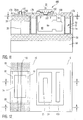
- Figure 11 illustrates in cross section a completed device of each type.
- Figure 12 illustrates in plan view the portion shown in Figures 1 - 10.
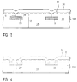
- FIGS 13 and 14 illustrate steps in an alternative embodiment of the invention.
- a p-type silicon substrate 100 having an initial thickness tolerance of 0.5% and having a patterned oxide layer 20 on top of it.
- This oxide layer having a nominal thickness of 2500 ⁇ , has been grown by a conventional method such as oxidation in steam and patterned by etching using a conventional reactive ion etch (RIE) process or a wet etch in BHF to form oxide islands 20 that will be used to separate and insulate the thin layers that will be formed for the field effect transistors, (FETs, generically referred to as CMOS and including both P-channel and N-channel FETs).
- RIE reactive ion etch
- FETs field effect transistors
- an epitaxial layer 30 of silicon having a nominal thickness of 5 ⁇ , has been grown enclosing the several oxide islands 20.
- This epitaxial layer 30 has been grown using the known technique of epitaxial lateral overgrowth as disclosed in G. Shahidi, et al "Fabrication of CMOS on Ultrathin SOI Obtained by Epitaxial Lateral Overgrowth and Chemical-Mechanical Polishing", IEDM technical digest, Dec, 1990 pp 587-590, in which the epitaxial layer starts from the areas between the oxide islands grows up and then grows laterally to meet above the oxide islands at an epitaxial join interface in the region denoted by the numeral 45.
- a solid phase epitaxy process such as that illustrated in "Influence of Si Film Thickness on Growth Enhancement in Si Lateral Solid Phase Epitaxy", by M. Moniwa, et al in Appl. Phys. Lett. 52(21), May 1988, pp. 1788-1790, may be used.
- the crystal quality is not as high as it is in the rest of the epitaxial layer because there are dislocations and "twins" where the two pieces of silicon meet. It is an advantageous feature of the invention that this relatively low quality area is not used to form transistors.
- the epi surface (the first top surface) has been planarized by a conventional polishing step such as that illustrated in the Shahidi reference, which also eliminates any notch that may have formed in area 40 where the two sides of the epitaxial overgrowth meet.
- the polysilicon may be recrystallised in a high temperature anneal, in which the crystal structure in the epitaxial layer will transfer to the recrystallized material.
- the bracket denoted 32 extending to the base of oxide 50 represents the extra thickness of epi required to give the correct epi depth for the bipolar transistors.
- the lower bipolar thickness a corresponding upper bipolar thickness being the sum of the thickness of islands 20 and the thickness denoted by bracket 32 of the silicon film above the islands.
- the first substrate 100 has been inverted and a second silicon substrate 60 has been bonded to the first substrate using oxide layer 50 as the bonding layer in a conventional process of heating the wafers in an oxygen ambient at 1100°C or less for several hours.
- oxide layer 50 as the bonding layer in a conventional process of heating the wafers in an oxygen ambient at 1100°C or less for several hours.
- oxide 55 has been removed. It served to protect the underlying silicon from metallic or other contamination during the bonding step.
- Fig 5 shows the result after a silicon removal step in which layer 100 (the former substrate in Fig 1) has been ground and/or etched and/or polished down to leave a thinner layer 110, of thickness about 2-3 ⁇ m, in areas 115 where the bipolar devices will be formed.
- the thickness of the silicon over islands 20 at this stage is a nominal 1 ⁇ m.
- a step of etching apertures 70 down to oxide islands 20, using the oxide as an etch stop in a highly selective silicon to oxide etch process, such as a CrO2 acid wet etch or a Cl2/SF6 dry etch has been performed.
- Islands 20 extend perpendicular to the plane of the paper and the cross sections of Figs 1 - 10 are taken through line A-A in the plan view of Fig 12.
- line A-A has been taken through one edge of the islands 20, in order to show that rectangular aperture 70 occupies only a portion of the island, leaving room for a CMOS transistor in front of or behind the plane of the paper.
- one or two polish stop pads may be used on an island.
- one of islands 20 has been shown without an aperture 70, in order to illustrate that an aperture 70' may be behind the plane of the paper (on the opposite edge from line A-A), or that if the islands are sufficiently close together, not all of them need to have polish stops.
- a conformal (low pressure CVD) layer of nitride (Si3N4) 80 having a nominal thickness of 1000 ⁇ is deposited over the whole wafer as shown in Fig. 7.
- a 1.5 ⁇ m layer of photoresist has been deposited and etched back in a conventional process using O2 plasma to leave resist only inside aperture 70.
- the portion of nitride layer 80 not protected by photoresist 90, including the sidewalls will be stripped in a CF4 reactive ion etch step.
- An optical emission end point plus a fixed amount of overetch to allow for tolerance in the etch process is used to insure that the nitride on the sidewalls is etched away, leaving a small aperture denoted by the numeral 95.
- a wet step with hot phosphoric acid may be used. Then, the remaining resist 90 in Fig.
- nitride in apertures 70 is removed, leaving nitride in apertures 70 to act as polish stops for the final polishing of silicon layer 110.
- a conventional chemical- mechanical polishing step such as that illustrated in U. S. Patent 4,735, 679, is performed in which the remainder of silicon layer 110 is thinned down until the top surface is coplanar with the nitride stops 85.
- the global planarity tolerance after this step is +100 ⁇ or better.
- a set of deep trenches 10 have been cut by a reactive ion etch step ( using SF6 + O2 plasma ) down to oxide layer 50. These deep trenches surround and isolate the bipolar devices in regions 115, as can be seen in Figs 11 and 12.
- the remainder of the trench formation, including providing a sidewall liner of thermal oxide, filling the trench with polysilicon, and growing a cap of oxide is conventional and well known to those skilled in the art.
- the CMOS devices will be formed in the thin silicon layers above oxide 20, which may be formed into silicon mesas by shallow isolation trenches.
- the bipolar circuits will be formed in the thicker portions 115.
- the deep trenches not only provide electrical isolation for the bipolar transistors, they also prevent crystal defects in regions 45 from propagating into the bipolar transistor regions.
- the nitride plates 85 are removed in order to avoid excessive stress on the silicon layer covering the rest of the oxide island.
- This technique therefore facilitates the coexistence of thin SOI regions for CMOS and thick SOI regions for bipolar in order to achieve optimal performance for BiCMOS circuits.
- Fig. 11 is a cross section taken through line B-B of Fig. 12 and Fig. 12 is a plan view taken through line C-C in Fig 11, showing the layout at the silicon surface.
- two polish stop pads 85 are shown, on either side of the island 20.
- An n-MOS transistor 150 having gate 155 and source/drain area 26 is shown on the left.
- a conventional NPN bipolar transistor 180 On the right of Fig. 12, surrounded by deep trench 10, a conventional NPN bipolar transistor 180 has emitter 197, base 192 and vertical collector extension 190, connected to buried conductive layer 18.
- Layer 18 is doped using a high energy ion implantation step (Mitsubishi Electric Corp.
- a conventional field oxide 170 surrounds the transistors.
- a shallow trench 87 may be formed in the space left after removing nitride pads 85 and in a strip connecting pads 85.
- pads 85 might have the shape of a hollow rectangle surrounding the transistor site, so that removal of the polish stops and refill with CVD oxide automatically forms the shallow trench isolation.
- bipolar and CMOS devices be positioned adjacent to one another as shown in the figures, which are drawn to illustrate the process, not any particular circuit layout, and there may be portions of circuits that have large numbers of bipolars without CMOS and vice versa.
- the layout of the polish stops is meant to be illustrative only. Those skilled in the art will readily be able to devise layouts suited to their purposes in order to achieve planarity and the required SOI thickness uniformity.
- the islands are simply omitted or small islands designed only to hold polish stops may be inserted in order to maintain the planarity of these regions.
- large oxide pads may be grown that will hold a number of transistors.
- both the islands and the bipolar regions will have varying dimensions. Since large pads will not be filled in during the epitaxial lateral overgrowth step, the process alternative of filling in the exposed back side of the oxide layer 20 with a polysilicon layer will be used in order to maintain the planarity of bonding oxide 50 in Figure 3.
- Bracket 13 there is shown a cross section of a wafer in an alternative step of Figure 2.
- Epi layer 30 has been grown to a thickness greater than that indicated by the bracket labelled 33, which represents a bonding silicon surface 37 (after a planarization step) that will be the interface with bonding layer 50 in Fig 4.
- the initial epi thickness is chosen to leave a thickness indicated by the bracket 32 that allows for the desired greater lower bipolar thickness of silicon in areas 115.
- distance 32 is 1.5 ⁇ m.
- a filler layer 35 of poly is deposited to fill in the notch above islands 20. When the top surface in Figure 13 is polished to prepare for the bonding operation, there will be a small amount of poly above the islands.
- the filler layer is recrystallized as described above in order to eliminate planarity problems from differential oxide growth on polysilicon and monocrystalline silicon.
- Figure 14 illustrates another alternative, suitable for applications where there are many CMOS devices close together, so that it is not practical to attempt to have the sides of the epi overgrowth meet.
- CMOS memory array of 100x100 transistors it is obviously impractical to grow the epi so that it extends to meet in the center of an enormous island.
- the epi is grown only thick enough to provide the required distance 32, covering only the edges of island 20' and the filler layer of poly is deposited directly on the oxide and recrystallization is used as before.
Landscapes
- Element Separation (AREA)
- Metal-Oxide And Bipolar Metal-Oxide Semiconductor Integrated Circuits (AREA)
- Bipolar Transistors (AREA)
- Thin Film Transistor (AREA)
Applications Claiming Priority (2)
| Application Number | Priority Date | Filing Date | Title |
|---|---|---|---|
| US884510 | 1992-05-15 | ||
| US07/884,510 US5258318A (en) | 1992-05-15 | 1992-05-15 | Method of forming a BiCMOS SOI wafer having thin and thick SOI regions of silicon |
Publications (3)
| Publication Number | Publication Date |
|---|---|
| EP0570043A2 true EP0570043A2 (de) | 1993-11-18 |
| EP0570043A3 EP0570043A3 (de) | 1993-11-24 |
| EP0570043B1 EP0570043B1 (de) | 1996-07-24 |
Family
ID=25384782
Family Applications (1)
| Application Number | Title | Priority Date | Filing Date |
|---|---|---|---|
| EP93201175A Expired - Lifetime EP0570043B1 (de) | 1992-05-15 | 1993-04-22 | SOI-Scheibe für BICMOS mit dünnen und dicken SOI-Siliziumgebieten |
Country Status (4)
| Country | Link |
|---|---|
| US (1) | US5258318A (de) |
| EP (1) | EP0570043B1 (de) |
| JP (1) | JP2654332B2 (de) |
| DE (1) | DE69303764T2 (de) |
Cited By (2)
| Publication number | Priority date | Publication date | Assignee | Title |
|---|---|---|---|---|
| EP0658930A3 (de) * | 1993-06-24 | 1997-10-01 | Texas Instruments Inc | Verfahren zum Varieren der Dicke der Oberfläche einer Siliziumschicht für ein Substrat vom SOI-Type. |
| EP1067600A1 (de) * | 1999-07-06 | 2001-01-10 | ELMOS Semiconductor AG | CMOS kompatibler SOI-Prozess |
Families Citing this family (45)
| Publication number | Priority date | Publication date | Assignee | Title |
|---|---|---|---|---|
| US5561073A (en) * | 1992-03-13 | 1996-10-01 | Jerome; Rick C. | Method of fabricating an isolation trench for analog bipolar devices in harsh environments |
| US5356822A (en) * | 1994-01-21 | 1994-10-18 | Alliedsignal Inc. | Method for making all complementary BiCDMOS devices |
| US5599728A (en) * | 1994-04-07 | 1997-02-04 | Regents Of The University Of California | Method of fabricating a self-aligned high speed MOSFET device |
| US5489792A (en) * | 1994-04-07 | 1996-02-06 | Regents Of The University Of California | Silicon-on-insulator transistors having improved current characteristics and reduced electrostatic discharge susceptibility |
| KR0142797B1 (ko) * | 1994-06-17 | 1998-08-17 | 문정환 | 실리콘-온-인슐레이터구조의 제조방법 |
| US5637513A (en) * | 1994-07-08 | 1997-06-10 | Nec Corporation | Fabrication method of semiconductor device with SOI structure |
| DE4433845A1 (de) * | 1994-09-22 | 1996-03-28 | Fraunhofer Ges Forschung | Verfahren zur Herstellung einer dreidimensionalen integrierten Schaltung |
| US5481126A (en) * | 1994-09-27 | 1996-01-02 | Purdue Research Foundation | Semiconductor-on-insulator electronic devices having trench isolated monocrystalline active regions |
| US5494837A (en) * | 1994-09-27 | 1996-02-27 | Purdue Research Foundation | Method of forming semiconductor-on-insulator electronic devices by growing monocrystalline semiconducting regions from trench sidewalls |
| DE4440362A1 (de) * | 1994-11-11 | 1996-05-15 | Telefunken Microelectron | Verfahren zum Herstellen integrierter Schaltungen mit passiven Bauelementen hoher Güte |
| US5872733A (en) * | 1995-06-06 | 1999-02-16 | International Business Machines Corporation | Ramp-up rate control circuit for flash memory charge pump |
| US5567631A (en) * | 1995-11-13 | 1996-10-22 | Taiwan Semiconductor Manufacturing Company | Method of forming gate spacer to control the base width of a lateral bipolar junction transistor using SOI technology |
| US5614431A (en) * | 1995-12-20 | 1997-03-25 | International Business Machines Corporation | Method of making buried strap trench cell yielding an extended transistor |
| US5728613A (en) * | 1996-03-27 | 1998-03-17 | Taiwan Semiconductor Manufacturing Company, Ltd. | Method of using an insulator spacer to form a narrow base width lateral bipolar junction transistor |
| JPH10223551A (ja) * | 1997-02-12 | 1998-08-21 | Nec Corp | Soi基板の製造方法 |
| US5952695A (en) * | 1997-03-05 | 1999-09-14 | International Business Machines Corporation | Silicon-on-insulator and CMOS-on-SOI double film structures |
| US5889293A (en) * | 1997-04-04 | 1999-03-30 | International Business Machines Corporation | Electrical contact to buried SOI structures |
| US6160292A (en) * | 1997-04-23 | 2000-12-12 | International Business Machines Corporation | Circuit and methods to improve the operation of SOI devices |
| US6133608A (en) * | 1997-04-23 | 2000-10-17 | International Business Machines Corporation | SOI-body selective link method and apparatus |
| US6410369B1 (en) | 1998-04-22 | 2002-06-25 | International Business Machines Corporation | Soi-body selective link method and apparatus |
| US6097056A (en) * | 1998-04-28 | 2000-08-01 | International Business Machines Corporation | Field effect transistor having a floating gate |
| WO1999059203A1 (en) * | 1998-05-08 | 1999-11-18 | Infineon Technologies Ag | Substrate and method for manufacturing the same |
| US6015745A (en) * | 1998-05-18 | 2000-01-18 | International Business Machines Corporation | Method for semiconductor fabrication |
| JP2000106333A (ja) * | 1998-09-29 | 2000-04-11 | Sony Corp | Soi構造を有する半導体基板の製造方法及び半導体装置の製造方法 |
| KR100281907B1 (ko) * | 1998-10-29 | 2001-02-15 | 김덕중 | 인텔리전트 전력 집적 회로 및 이를 제조하는 방법 |
| US6353246B1 (en) | 1998-11-23 | 2002-03-05 | International Business Machines Corporation | Semiconductor device including dislocation in merged SOI/DRAM chips |
| KR20000040104A (ko) | 1998-12-17 | 2000-07-05 | 김영환 | 실리콘 온 인슐레이터 웨이퍼의 제조방법 |
| US6214653B1 (en) | 1999-06-04 | 2001-04-10 | International Business Machines Corporation | Method for fabricating complementary metal oxide semiconductor (CMOS) devices on a mixed bulk and silicon-on-insulator (SOI) substrate |
| US6372600B1 (en) * | 1999-08-30 | 2002-04-16 | Agere Systems Guardian Corp. | Etch stops and alignment marks for bonded wafers |
| JP4202563B2 (ja) | 1999-11-18 | 2008-12-24 | 株式会社東芝 | 半導体装置 |
| TW478095B (en) * | 1999-12-09 | 2002-03-01 | United Microelectronics Corp | Manufacture method of isolation trench for bipolar complementary transistor |
| US6486043B1 (en) | 2000-08-31 | 2002-11-26 | International Business Machines Corporation | Method of forming dislocation filter in merged SOI and non-SOI chips |
| US6555891B1 (en) | 2000-10-17 | 2003-04-29 | International Business Machines Corporation | SOI hybrid structure with selective epitaxial growth of silicon |
| JP2004103946A (ja) * | 2002-09-11 | 2004-04-02 | Canon Inc | 基板及びその製造方法 |
| DE102004005506B4 (de) * | 2004-01-30 | 2009-11-19 | Atmel Automotive Gmbh | Verfahren zur Erzeugung von aktiven Halbleiterschichten verschiedener Dicke in einem SOI-Wafer |
| US20060261436A1 (en) * | 2005-05-19 | 2006-11-23 | Freescale Semiconductor, Inc. | Electronic device including a trench field isolation region and a process for forming the same |
| US7491622B2 (en) | 2006-04-24 | 2009-02-17 | Freescale Semiconductor, Inc. | Process of forming an electronic device including a layer formed using an inductively coupled plasma |
| US7670895B2 (en) | 2006-04-24 | 2010-03-02 | Freescale Semiconductor, Inc | Process of forming an electronic device including a semiconductor layer and another layer adjacent to an opening within the semiconductor layer |
| US7528078B2 (en) | 2006-05-12 | 2009-05-05 | Freescale Semiconductor, Inc. | Process of forming electronic device including a densified nitride layer adjacent to an opening within a semiconductor layer |
| JP5066936B2 (ja) * | 2007-02-22 | 2012-11-07 | 信越半導体株式会社 | Soiウエーハの製造方法 |
| WO2015135784A2 (en) | 2014-03-12 | 2015-09-17 | Koninklijke Philips N.V. | Ultrasound transducer assembly and method for manufacturing an ultrasound transducer assembly |
| US11393806B2 (en) | 2019-09-23 | 2022-07-19 | Analog Devices, Inc. | Gallium nitride and silicon carbide hybrid power device |
| US11195715B2 (en) * | 2020-03-17 | 2021-12-07 | Globalfoundries U.S. Inc. | Epitaxial growth constrained by a template |
| CN113664694A (zh) * | 2021-07-29 | 2021-11-19 | 山西烁科晶体有限公司 | 碳化硅双面抛光中硅面及碳面去除厚度的测定方法 |
| CN116626922B (zh) * | 2023-07-24 | 2023-10-27 | 福建玻尔光电科技有限责任公司 | 内置电极式薄膜铌酸锂电光调制器的制备方法 |
Family Cites Families (26)
| Publication number | Priority date | Publication date | Assignee | Title |
|---|---|---|---|---|
| GB1186340A (en) * | 1968-07-11 | 1970-04-02 | Standard Telephones Cables Ltd | Manufacture of Semiconductor Devices |
| US3929528A (en) * | 1973-01-12 | 1975-12-30 | Motorola Inc | Fabrication of monocriptalline silicon on insulating substrates utilizing selective etching and deposition techniques |
| NL7710164A (nl) * | 1977-09-16 | 1979-03-20 | Philips Nv | Werkwijze ter behandeling van een eenkristal- lijn lichaam. |
| US4549926A (en) * | 1982-01-12 | 1985-10-29 | Rca Corporation | Method for growing monocrystalline silicon on a mask layer |
| US4507158A (en) * | 1983-08-12 | 1985-03-26 | Hewlett-Packard Co. | Trench isolated transistors in semiconductor films |
| US4554059A (en) * | 1983-11-04 | 1985-11-19 | Harris Corporation | Electrochemical dielectric isolation technique |
| JPS60144949A (ja) * | 1984-01-06 | 1985-07-31 | Nec Corp | 半導体装置の製造方法 |
| US4615762A (en) * | 1985-04-30 | 1986-10-07 | Rca Corporation | Method for thinning silicon |
| JPS6321631A (ja) * | 1986-07-15 | 1988-01-29 | Olympus Optical Co Ltd | 絞り駆動装置 |
| JPS6350791A (ja) * | 1986-08-20 | 1988-03-03 | 株式会社東芝 | 高速増殖炉の安全容器 |
| NL8700033A (nl) * | 1987-01-09 | 1988-08-01 | Philips Nv | Werkwijze voor het vervaardigen van een halfgeleiderinrichting van het type halfgeleider op isolator. |
| US4735679A (en) * | 1987-03-30 | 1988-04-05 | International Business Machines Corporation | Method of improving silicon-on-insulator uniformity |
| US4760036A (en) * | 1987-06-15 | 1988-07-26 | Delco Electronics Corporation | Process for growing silicon-on-insulator wafers using lateral epitaxial growth with seed window oxidation |
| US4902641A (en) * | 1987-07-31 | 1990-02-20 | Motorola, Inc. | Process for making an inverted silicon-on-insulator semiconductor device having a pedestal structure |
| US4897362A (en) * | 1987-09-02 | 1990-01-30 | Harris Corporation | Double epitaxial method of fabricating semiconductor devices on bonded wafers |
| JPH01106466A (ja) * | 1987-10-19 | 1989-04-24 | Fujitsu Ltd | 半導体装置の製造方法 |
| JPH067594B2 (ja) * | 1987-11-20 | 1994-01-26 | 富士通株式会社 | 半導体基板の製造方法 |
| NL8801981A (nl) * | 1988-08-09 | 1990-03-01 | Philips Nv | Werkwijze voor het vervaardigen van een halfgeleiderinrichting. |
| US5051378A (en) * | 1988-11-09 | 1991-09-24 | Sony Corporation | Method of thinning a semiconductor wafer |
| US4908328A (en) * | 1989-06-06 | 1990-03-13 | National Semiconductor Corporation | High voltage power IC process |
| JPH0324719A (ja) * | 1989-06-22 | 1991-02-01 | Canon Inc | 単結晶膜の形成方法及び結晶物品 |
| US4923826A (en) * | 1989-08-02 | 1990-05-08 | Harris Corporation | Method for forming dielectrically isolated transistor |
| JPH0636414B2 (ja) * | 1989-08-17 | 1994-05-11 | 信越半導体株式会社 | 半導体素子形成用基板の製造方法 |
| US5081061A (en) * | 1990-02-23 | 1992-01-14 | Harris Corporation | Manufacturing ultra-thin dielectrically isolated wafers |
| US5034343A (en) * | 1990-03-08 | 1991-07-23 | Harris Corporation | Manufacturing ultra-thin wafer using a handle wafer |
| US5143862A (en) * | 1990-11-29 | 1992-09-01 | Texas Instruments Incorporated | SOI wafer fabrication by selective epitaxial growth |
-
1992
- 1992-05-15 US US07/884,510 patent/US5258318A/en not_active Expired - Lifetime
-
1993
- 1993-04-14 JP JP5111104A patent/JP2654332B2/ja not_active Expired - Lifetime
- 1993-04-22 EP EP93201175A patent/EP0570043B1/de not_active Expired - Lifetime
- 1993-04-22 DE DE69303764T patent/DE69303764T2/de not_active Expired - Fee Related
Cited By (2)
| Publication number | Priority date | Publication date | Assignee | Title |
|---|---|---|---|---|
| EP0658930A3 (de) * | 1993-06-24 | 1997-10-01 | Texas Instruments Inc | Verfahren zum Varieren der Dicke der Oberfläche einer Siliziumschicht für ein Substrat vom SOI-Type. |
| EP1067600A1 (de) * | 1999-07-06 | 2001-01-10 | ELMOS Semiconductor AG | CMOS kompatibler SOI-Prozess |
Also Published As
| Publication number | Publication date |
|---|---|
| JPH07254653A (ja) | 1995-10-03 |
| EP0570043B1 (de) | 1996-07-24 |
| JP2654332B2 (ja) | 1997-09-17 |
| DE69303764D1 (de) | 1996-08-29 |
| EP0570043A3 (de) | 1993-11-24 |
| DE69303764T2 (de) | 1997-02-06 |
| US5258318A (en) | 1993-11-02 |
Similar Documents
| Publication | Publication Date | Title |
|---|---|---|
| EP0570043B1 (de) | SOI-Scheibe für BICMOS mit dünnen und dicken SOI-Siliziumgebieten | |
| US6211039B1 (en) | Silicon-on-insulator islands and method for their formation | |
| US5910018A (en) | Trench edge rounding method and structure for trench isolation | |
| JP4322453B2 (ja) | 半導体装置およびその製造方法 | |
| US7095081B2 (en) | Semiconductor device and manufacturing method thereof | |
| KR100333582B1 (ko) | SOI상의 실리콘-게르마늄 BiCMOS 집적회로 형성방법 및 그 집적회로 | |
| US4963505A (en) | Semiconductor device and method of manufacturing same | |
| US5318663A (en) | Method for thinning SOI films having improved thickness uniformity | |
| US5436173A (en) | Method for forming a semiconductor on insulator device | |
| US6074932A (en) | Method for forming a stress-free shallow trench isolation | |
| US5334281A (en) | Method of forming thin silicon mesas having uniform thickness | |
| US7525156B2 (en) | Shallow trench isolation fill by liquid phase deposition of SiO2 | |
| JP3014012B2 (ja) | 半導体装置の製造方法 | |
| US6046477A (en) | Dense SOI programmable logic array structure | |
| US6204098B1 (en) | Method of formation in a silicon wafer of an insulated well | |
| KR100529633B1 (ko) | 에피택셜 실리콘을 이용한 반도체 소자 및 그 제조 방법 | |
| US5909626A (en) | SOI substrate and fabrication process therefor | |
| US4571818A (en) | Isolation process for high-voltage semiconductor devices | |
| US7541258B2 (en) | Method of manufacturing semiconductor substrate and method of manufacturing semiconductor device | |
| EP0661735B1 (de) | Verfahren zur Herstellung integrierter Schaltungen, insbesondere intelligenter Leistungsanordnungen | |
| JP2839088B2 (ja) | 半導体装置 | |
| EP0929095B1 (de) | Verfahren zur Herstellung eines SOI-Substrates | |
| US7425495B2 (en) | Method of manufacturing semiconductor substrate and semiconductor device | |
| KR100257758B1 (ko) | 이중실리콘 기판 및 그를 사용한 반도체소자 제조방법 | |
| US20020072237A1 (en) | Method for unpatterned resist etch back of shallow trench isolation refill insulator |
Legal Events
| Date | Code | Title | Description |
|---|---|---|---|
| PUAI | Public reference made under article 153(3) epc to a published international application that has entered the european phase |
Free format text: ORIGINAL CODE: 0009012 |
|
| PUAL | Search report despatched |
Free format text: ORIGINAL CODE: 0009013 |
|
| AK | Designated contracting states |
Kind code of ref document: A2 Designated state(s): DE FR GB |
|
| AK | Designated contracting states |
Kind code of ref document: A3 Designated state(s): DE FR GB |
|
| 17P | Request for examination filed |
Effective date: 19940324 |
|
| 17Q | First examination report despatched |
Effective date: 19950809 |
|
| GRAH | Despatch of communication of intention to grant a patent |
Free format text: ORIGINAL CODE: EPIDOS IGRA |
|
| GRAH | Despatch of communication of intention to grant a patent |
Free format text: ORIGINAL CODE: EPIDOS IGRA |
|
| GRAA | (expected) grant |
Free format text: ORIGINAL CODE: 0009210 |
|
| AK | Designated contracting states |
Kind code of ref document: B1 Designated state(s): DE FR GB |
|
| PG25 | Lapsed in a contracting state [announced via postgrant information from national office to epo] |
Ref country code: FR Effective date: 19960724 |
|
| REF | Corresponds to: |
Ref document number: 69303764 Country of ref document: DE Date of ref document: 19960829 |
|
| EN | Fr: translation not filed | ||
| PG25 | Lapsed in a contracting state [announced via postgrant information from national office to epo] |
Ref country code: GB Effective date: 19970422 |
|
| PLBE | No opposition filed within time limit |
Free format text: ORIGINAL CODE: 0009261 |
|
| STAA | Information on the status of an ep patent application or granted ep patent |
Free format text: STATUS: NO OPPOSITION FILED WITHIN TIME LIMIT |
|
| 26N | No opposition filed | ||
| GBPC | Gb: european patent ceased through non-payment of renewal fee |
Effective date: 19970422 |
|
| PG25 | Lapsed in a contracting state [announced via postgrant information from national office to epo] |
Ref country code: DE Free format text: LAPSE BECAUSE OF NON-PAYMENT OF DUE FEES Effective date: 19980101 |