EP0570164B1 - Verschachteltes Speichersystem - Google Patents
Verschachteltes Speichersystem Download PDFInfo
- Publication number
- EP0570164B1 EP0570164B1 EP93303547A EP93303547A EP0570164B1 EP 0570164 B1 EP0570164 B1 EP 0570164B1 EP 93303547 A EP93303547 A EP 93303547A EP 93303547 A EP93303547 A EP 93303547A EP 0570164 B1 EP0570164 B1 EP 0570164B1
- Authority
- EP
- European Patent Office
- Prior art keywords
- memory
- data
- address
- bus
- clk
- Prior art date
- Legal status (The legal status is an assumption and is not a legal conclusion. Google has not performed a legal analysis and makes no representation as to the accuracy of the status listed.)
- Expired - Lifetime
Links
Images

















Classifications
-
- G—PHYSICS
- G06—COMPUTING OR CALCULATING; COUNTING
- G06F—ELECTRIC DIGITAL DATA PROCESSING
- G06F12/00—Accessing, addressing or allocating within memory systems or architectures
- G06F12/02—Addressing or allocation; Relocation
- G06F12/06—Addressing a physical block of locations, e.g. base addressing, module addressing, memory dedication
- G06F12/0607—Interleaved addressing
-
- F—MECHANICAL ENGINEERING; LIGHTING; HEATING; WEAPONS; BLASTING
- F02—COMBUSTION ENGINES; HOT-GAS OR COMBUSTION-PRODUCT ENGINE PLANTS
- F02B—INTERNAL-COMBUSTION PISTON ENGINES; COMBUSTION ENGINES IN GENERAL
- F02B75/00—Other engines
- F02B75/02—Engines characterised by their cycles, e.g. six-stroke
- F02B2075/022—Engines characterised by their cycles, e.g. six-stroke having less than six strokes per cycle
- F02B2075/025—Engines characterised by their cycles, e.g. six-stroke having less than six strokes per cycle two
Definitions
- the present invention relates to an interleaving memory which enables a high-speed-data-output.
- a high-speed data processing such that meets today's needs necessitates a high-speed-memory-readout which is by no means easy to realize; for it unavoidably takes a certain time, or a cycle time (Tc) for memory access.
- Tc cycle time
- interleaving memory consists of n data banks so that the access width thereof becomes n times as wide as that of a data bus to reduce Tc to Tc/n, thereby increasing the memory-readout speed for sequential addressing [for further information, see "Handbook of Electric Data Transmission", page 1667, 1988, Ohm-sha].
- Fig. 1 Depicted in Fig. 1 are a 2-way interleaving memory and a calculator.
- the interleaving memory comprises a first memory 301 and a second memory 302, each consisting of a 0-bank and a 1-bank which store data at even-numbered addresses and odd-numbered addresses respectively.
- a calculator 303 carries out arithmetic logic operations (hereinafter, simply referred to as arithmetic operations) of data inputted thereto from the first memory 301 by way of a first bus 304, and from the second memory 302 by way of a second bus 305.
- arithmetic logic operations hereinafter, simply referred to as arithmetic operations
- first memory 301 data are read out from the 0-bank and 1-bank in the same Tc's, and inputted into the first bus 304 sequentially. For example, when address 2n is assigned as a starting address, data at address 2n and the following address 2n+1 are read out in the same Tc; the former are inputted into the first bus 304, and the latter are done so immediately without being read out when address 2n+1 is assigned subsequently, thereby reducing Tc and hence the memory-readout time by half.
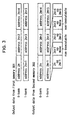
- second memory 302 data are read out and inputted into the second bus 305 synchronously with the first memory 301 in the same manner. As a result, data at contiguous addresses are steadily inputted from each memory into the calculator 303 twice as fast as non-interleaving memories, the illustration of which is shown in Fig. 2.
- the calculator 303 carries out arithmetic operations of data at addresses : (2n, 2m), (2n+1, 2m+1), (2n+2, 2m+2), (2n+3, 2m+3), ... twice as fast as the non-interleaving memories.
- the interleaving memory makes it possible to increase the memory-readout speed hence data processing speed twice as fast.
- the data are inputted into the calculator 303 consecutively in the same manner as explained in the above, but the calculator 303 carries out arithmetic operations of data at addresses : (2n, 2m+1), (2n+1, 2m+2), (2n+2, 2m+3), ...
- the calculator 303 carries out arithmetic operations of data at addresses : (2n, 2m+1), (2n+1, 2m+2), (2n+2, 2m+3), ...
- not all the data at addresses in brackets are read out in the same Tc's.
- data at addresses (2n, 2m+1) are read out in the same Tc, but are not the data at the following addresses (2n+1, 2m+2); data at address 2m+2 are read out one Tc behind those at address 2n+1. Therefore, in every other operation, data from the second memory 302 have not been read out when the calculator 303 is to carry out the arithmetic operation. For this reason, calculator 303 can carry out only one arithmetic operation per
- a conventional interleaved memory is described in PROCEEDINGS OF THE 1989 INTERNATIONAL CONFERENCE ON PARALLEL PROCESSING, Vol. 1 Architecture, 8 th August 1989, PA US, pp.242-6, Rau et al. "The CYDRA 5 Stride-Insensitive Memory System".
- the memory is arranged in such a way that it is insensitive to the size of the working data set and the manner in which data are placed in the memory and accessed by a program.
- the memory uses buffers at the input to queue up requests to busy modules so that the processor does not need to wait thereby reducing contention delays.
- data in the memory is arranged in a carefully engineered pseudo-random fashion to deal with variable stride accesses.
- EP-A-0 384 620 Another conventional interleaved memory is described in European patent application EP-A-0 384 620.
- the memory has two memory banks and corresponding error correction circuitry.
- the data is read out of the two memory banks simultaneously and error corrected.
- Latches provided at the error correction circuitry then introduce a delay of one cycle period in one of the data outputs to create an offset between the output of the two data. In this way the data can be placed on the same bus in a sequential manner.
- a further conventional multiple module (non-interleaved) memory and a method of accessing the same are described in IEEE Transactions on Computers, Vol. C-36, No.12, December 1987, pp.1440-49, D.T.Harper and J.R.Jump: "Vector Access Performance in Parallel Memories Using a Skewed Storage Scheme".
- Each module of the memory comprises input and output buffers such that transient non-uniformities which occur in some access patterns do not degrade performance.
- a skewing scheme is used to map vector components into parallel memory modules such that, for most vector access patterns, the number of memory conflicts are reduced over that observed in parallel interleaved memory systems.
- the present invention has an object to provide an interleaving memory which can increase the data processing speed even when data used for the arithmetic operations are read out in different Tc's.
- a high-speed output interleaving memory for steadily outputting data held at contiguous addresses in the memory
- the memory comprising: first memory means comprising n data banks and arranged to output n units of sequentially addressed data simultaneously; and second memory means comprising n data banks and arranged to output n units of sequentially addressed data simultaneously; characterised in that the memory further comprises: holding means for holding n-1 units of data read out from a selected n-1 banks of the first memory means or the second memory means, the holding means being arranged to delay output of the n-1 held units of data for 1/n of the memory access cycle period; and controlling means for controlling the holding means so as to match the data-output timing of one memory means with that of the data read out in a later memory access cycle period of the other memory means.
- the first memory means comprises a 0-bank and a 1-bank for simultaneously outputting data units at even-numbered addresses from the 0-bank and data units at odd-numbered addresses from the 1-bank
- the second memory means comprises a 0-bank and a 1-bank for simultaneously outputting data units at even-numbered addresses from the 0-bank and data units at odd-numbered addresses from the 1-bank.
- the high-speed output interleaving memory may further comprise a first selecting means for selecting data units from one of the 0-bank and the 1-bank of the first memory means, a second selecting means for selecting data units from one of the 0-bank and the 1-bank of the second memory means, a third selecting means for selecting data units from two of the first selecting means, the second selecting means, and the holding means, and wherein the controlling means is arranged to control the third selecting means to output data units of the first memory means in one of an ascending direction and a descending direction, and to output data units of the second memory means in one of the ascending direction and the descending direction.
- holding means can hold data from either bank of either memory to match the data-output timing thereof with that of the data read out in a later Tc.
- the interleaving memory of the present invention unlike conventional ones, enables a calculator to do the arithmetic operations twice as fast as the non-interleaving memories for sequential addressing regardless of data-readout timing.
- the interleaving memory comprises the following components : a first memory 101 and a second memory 201, each of which consisting of a 0-bank and a 1-bank for storing data at even-numbered addresses and odd-numbered addresses respectively; a first latch 102 which latches data from the 0-bank of the first memory 101 at the high level of CLK 2; a second latch 103 which latches data from the 1-bank of the first memory 101 at the high level of CLK 2; a third latch 202 which latches data from the 0-bank of the second memory 201 at the high level of CLK 2; a fourth latch 203 which latches data from the 1-bank of the second memory 201 at the high level of CLK 2; a first multiplexer 105(MUX 105) which selects data from either the first latch 102 or second latch 103; a fifth latch 106 which latches data from MUX 105 at the high level of CLK 1; a second multiplexer 205(MUX 205) which selects data from either the third
- the calculator 112 carries out arithmetic operations of the data inputted thereto from the first bus 111 and second bus 211. All these components are controlled by the control unit 114 with signals inputted thereinto and outputted therefrom as set forth in Table 1.
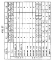
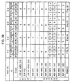
- INPUT/OUTPUT SIGNALS OF CONTROL UNIT 114 O U T P U T 1 First multiplexer controlling signal 104 (MUX CNTL 104) 2 Second multiplexer controlling signal 204 (MUX CNTL 204) 3 Third multiplexer controlling signal 107 (MUX CNTL 107) 4 Fourth multiplexer controlling signal 207 (MUX CNTL 207) 5 First multiplexer controlling signal 109 (BUS CNTL 109) 6 Second bus output-unit controlling ignal 209 (BUS CNTL 209) I N P U T 1 LSB (Least Significant Bit) of initial ADRS 113 2 LSB of initial ADRS 213 3 First direction modifying signal 115(DIR 115) 4 Second direction modifying signal 215(DIR 215) 5 Operation starting
- the control unit 114 controls the components with these output signals as follows:
- control unit 114 controls the components with these input signals as follows:
- Data from the second memory 201 are read out one Tc behind in Case 3, and those from the first memory 101 are read out one Tc behind in Case 4.
- Each case is subdivided by whether the addresses are to be incremented or decremented, and the starting addresses have an even-number or an odd-number. Particulars of all these 16 sub-cases are set forth as in Table 2.
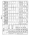
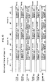
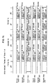
- the calculator 112 carries out the arithmetic operations of data read out in the same Tc from each memory in this case. (1-1) This is the case when the starting addresses of both the memories have even-numbers, and both of ADRS 113 and ADRS 213 are incremented by 2 at the rising edge of CLK 1 by an unillustrated addressing unit. Particulars of the input/output signals and data-output timing hereof are shown in Figs. 7 and 11 respectively.
- the initial ADRS 113 and ADRS 213 have 2's with 0-LSB's.
- data at address 2's of the 0-banks and those at the following address 3's of the 1-banks of both the memories are read out in the first Tc.
- data at address 2 and address 3 of the first memory 101 are latched by the first latch 102 and second latch 103 respectively, while those at address 2 and address 3 of the second memory 201 are done so by the third latch 202 and fourth latch 203 respectively.
- START 116 turns to 1, and the control unit 114 receives LSB's of the initial ADRS 113 and ADRS 213 having 0's, and DIR 115 and DIR 215 having 0's. Then, the control unit 114 outputs MUX CNTL 107 and MUX CNTL 207 having 2's at CLK 1, and 1's at CLK 2 in every Tc; BUS CNTL 109 having 0 at CLK 1 in the first Tc, and 1 at CLK 2 in the first Tc and afterwards; BUS CNTL 209 having 0 at CLK 1 in the first Tc, and 2 at CLK 2 in the first Tc and afterwards.
- data at address 2 of the first memory 101 are inputted into the first bus 111 by way of the first latch 102, MUX 108, and B_I/F 110, while those at address 2 of the second memory 201 into the second bus 211 by way of the third latch 202, MUX 208, and B_I/F 210 at CLK 2 in the first Tc.
- data at address 3 of the first memory 101 are inputted into the first bus 111 by way of the second latch 103, MUX 108, and B_I/F 110, while those at address 3 of the second memory 201 into the second bus 211 by way of the fourth latch 203, MUX 208, and B_I/F 210 at CLK 1 in the second Tc.
- data at even-numbered addresses of the first memory 101 are inputted into the first bus 111 and those at even-numbered addresses of the second memory 201 into the second bus 211 at CLK 2 in every Tc; data at odd-numbered addresses of the first memory 101 are inputted into the first bus 111 and those at odd-numbered addresses of the second memory 201 into the second bus 211 at CLK 1 in every Tc except the first Tc.
- the interleaving memory allows both the memories to output data at contiguous addresses into the first bus 111 and second bus 211 in matching Tc's, thereby enabling the calculator 112 to carry out arithmetic operations sequentially twice as fast as the non-interleaving memories.
- the starting addresses of both the memories be address 5's
- the initial ADRS 113 and ADRS 213 have 5's with 1-LSB's.
- data at address 5's of the 1-banks and those at the following address 4's of the 0-banks of both the memories are read out in the first Tc.
- data at address 4 and address 5 of the first memory 101 are latched by the first latch 102 and second latch 103 respectively, while those at address 4 and address 5 of the second memory 201 are done so by the third latch 202 and fourth latch 203 respectively.
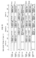
- START 116 turns to 1, and the control unit 114 receives LSB's of the initial ADRS 113 and ADRS 213 having 1's, and DIR 115 and DIR 215 having 1's. Then, the control unit 114 outputs MUX CNTL 107 and MUX CNTL 207 having 1's at CLK 1, and 2's at CLK 2 in every Tc; BUS CNTL 109 having 0 at CLK 1 in the first Tc, and 1 at CLK 2 in the first Tc and afterwards; BUS CNTL 209 having 0 at CLK 1 in the first Tc, and 2 at CLK 2 in the first Tc and afterwards.
- data at address 4 of the first memory 101 are inputted into the first bus 111 by way of the first latch 102, MUX 108, and B_I/F 110, while those of the second memory 201 into the second bus 211 by way of the third latch 202, MUX 208, and B_I/F 210 at CLK 1 in the second Tc.
- data at odd-numbered addresses of the first memory 101 are inputted into the first bus 111 and those at odd-numbered addresses of the second memory 201 into the second bus 211 at CLK 2 in every Tc; data at even-numbered addresses of the first memory 101 are inputted into the first bus 111 and those at even-numbered addresses of the second memory 201 into the second bus 211 at CLK 1 in every Tc except the first Tc.
- the interleaving memory allows both the memories to output data at contiguous addresses into the first bus 111 and second bus 211 in matching Tc's, thereby enabling the calculator 112 to carry out arithmetic operations sequentially twice as fast as the non-interleaving memories.
- the initial ADRS 113 has 2 with 0-LSB and the initial ADRS 213 has 5 with 1-LSB.
- data at address 2 of the 0-bank of the first memory 101 and those at the address 5 of the 1-bank of the second memory 201, as well as those at the following address 3 of the 1-bank of the first memory 101 and those at the following address 4 of the 0-bank of the second memory 201 are read out in the first Tc.
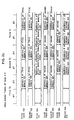
- START 116 turns to 1, and the control unit 114 receives LSB of the initial ADRS 113 having 0 and LSB of the initial ADRS 213 having 1, and DIR 115 having 0 and DIR 215 having 1. Then, the control unit 114 outputs MUX CNTL 107 having 2 and MUX CNTL 207 having 1 at CLK 1, and respectively 1 and 2 at CLK 2 in every Tc; BUS CNTL 109 having 0 at CLK 1 in the first Tc, and 1 at CLK 2 in the first Tc and afterwards; BUS CNTL 209 having 0 at CLK 1 in the first Tc, and 2 at CLK 2 in the first Tc and afterwards.
- data at address 2 of the first memory 101 are inputted into the first bus 111 by way of the first latch 102, MUX 108, and B_I/F 110, while those at address 5 of the second memory 201 into the second bus 211 by way of the fourth latch 203, MUX 208, and B_I/F 210 at CLK 2 in the first Tc.
- data at address 3 of the first memory 101 are inputted into the first bus 111 by way of the second latch 103, MUX 108 and B_I/F 110, while those at address 4 of the second memory 201 into the second bus 211 by way of the third latch 202, MUX 208, and B_I/F 210 at CLK 1 in the second Tc.
- data at even-numbered addresses of the first memory 101 are inputted into the first bus 111 and those at odd-numbered addresses of the second memory 201 into the second bus 211 at CLK 2 in every Tc; data at odd-numbered addresses of the first memory 101 are inputted into the first bus 111 and those at even-numbered addresses of the second memory 201 into the second bus 211 at CLK 1 in every Tc except the first Tc.
- the interleaving memory allows both the memories to output data at contiguous addresses into the first bus 111 and second bus 211 in matching Tc's, thereby enabling the calculator 112 to carry out arithmetic operations sequentially twice as fast as the non-interleaving memories.
- the initial ADRS 113 has 5 with 1-LSB and the initial ADRS 213 has 2 with 0-LSB.
- data at address 5 of the 1-bank of the first memory 101 and those at address 2 of the 0-bank of the second memory 201, as well as those at the following address 4 of the 0-bank of the first memory 101 and those at the following address 3 of the 1-bank of the second memory 201 are read out in the first Tc.
- the data at address 4 and address 5 of the first memory 101 are latched by the first latch 102 and second latch 103 respectively, while those at address 2 and address 3 of the second memory 201 are done so by the third latch 202 and fourth latch 203 respectively.
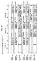
- START 116 turns to 1, and the control unit 114 receives LSB of the initial ADRS 113 having 1 and LSB of the initial ADRS 213 having 0, and DIR 115 having 1 and DIR 215 having 0. Then, the control unit 114 outputs MUX CNTL 107 having 1 and MUX CNTL 207 having 2 at CLK 1, and respectively 2 and 1 at CLK 2 in every Tc; BUS CNTL 109 having 0 at CLK 1 in the first Tc, and 1 at CLK 2 in the first Tc and afterwards; BUS CNTL 209 having 0 at CLK 1 in the first Tc, and 2 at CLK 2 in the first Tc and afterwards.
- data at address 5 of the first memory 101 are inputted into the first bus 111 by way of the second latch 103, MUX 108, and B_I/F 110, while those at address 2 of the second memory 201 into the second bus 211 by way of the third latch 202, MUX 208, and B_I/F 210 at CLK 2 in the first Tc.
- data at address 4 of the first memory 101 are inputted into the first bus 111 by way of the first latch 102, MUX 108, and B_I/F 110, while those at address 3 of the second memory 201 into the second bus 211 by way of the fourth latch 203, MUX 208, and B_I/F 210 at CLK 1 in the second Tc.
- data at odd-numbered addresses of the first memory 101 are inputted into the first bus 111 and those at even-numbered addresses of the second memory 201 into the second bus 211 at CLK 2 in every Tc; data at the even-numbered addresses of the first memory 101 are inputted into the first bus 111 and those at the odd-numbered addresses of the second memory 201 into the second bus 211 at CLK 1 in every Tc except the first Tc.
- the interleaving memory allows both the memories to output data at contiguous addresses into the first bus 111 and second bus 211 in matching Tc's, thereby enabling the calculator 112 to carry out arithmetic operations sequentially twice as fast as the non-interleaving memories.
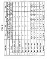
- the calculator 112 carries out the arithmetic operations of data read out in the same Tc from each memory, although the data at one of the addresses accessed in the first Tc in each memory are not inputted into the calculator 112. (2-1) This is the case when the starting addresses of both the memories have odd-numbers, and both ADRS 113 and ADRS 213 are incremented by 2 at the rising edge of CLK 1 by the unillustrated addressing unit. Particulars of the input/output signals and data-output timing hereof are shown in Figs. 8 and 15 respectively.
- both of the initial ADRS 113 and ADRS 213 have 3's with 1-LSB's.
- data at the preceding address 2's of the 0-banks and those at address 3's of the 1-banks of both the memories are read out in the first Tc.
- data at address 2 and address 3 of the first memory 101 are latched by the first latch 102 and second latch 103 respectively, while the data address 2 and address 3 of the second memory 201 are done so by the third latch 202 and fourth latch 203 respectively.
- START 116 turns to 1, and the control unit 114 receives LSB's of the initial ADRS 113 and ADRS 213 having 1's, and DIR 115 and DIR 215 having 0's. Then, the control unit 114 outputs MUX CNTL 107 and MUX CNTL 207 having 2's at CLK 1, and 1's at CLK 2 in every Tc; BUS CNTL 109 having 0 in the first Tc, and 1 in the second Tc and afterwards; BUS CNTL 209 having 0 in the first Tc, and 2 in the second Tc and afterwards.
- data at the following address 4 of the first memory 101 which have been read out at the second Tc, are inputted into the first bus 111 by way of the first latch 102, MUX 108, and B_I/F 110, while those at address 4 of the second memory 201 into the second bus 211 by way of the third latch 202, MUX 208, and B_I/F 210 at CLK 2 in the second Tc.
- data at odd-numbered addresses of the first memory 101 are inputted into the first bus 111 and data at odd-numbered addresses of the second memory 201 into the second bus 211 at CLK 1 in the second and the following Tc's; data at even-numbered addresses of the first memory 101 are inputted into the first bus 111 and data at even-numbered addresses of the second memory 201 into the second bus 211 at CLK 2 in the second and the following Tc's.
- the interleaving memory allows both the memories to output data at contiguous addresses into the first bus 111 and second bus 211 in matching Tc's, thereby enabling the calculator 112 to carry out arithmetic operations sequentially twice as fast as the non-interleaving memories.
- the starting addresses be address 4's
- the initial ADRS 113 and ADRS 213 have 4's with 0-LSB's.
- data at the preceding address 5's of the 1-banks and those at address 4's of the 0-banks of both the memories are read out in the first Tc.
- data at address 4 and address 5 of the first memory 101 are latched by the first latch 102 and second latch 103 respectively, while those at address 4 and address 5 of the second memory 201 are done so by the third latch 202 and fourth latch 203 respectively.
- START 116 turns to 1, and the control unit 114 receives LSB's of the initial ADRS 113 and ADRS 213 having 0's, and DIR 115 and DIR 215 having 1's. Then, the control unit 114 outputs MUX CNTL 107 and MUX CNTL 207 having 1's at CLK 1, and 2's at CLK 2 in every Tc; BUS CNTL 109 having 0 in the first Tc, and 1 in second Tc and afterwards; BUS CNTL 209 having 0 in the first Tc, and 2 in the second Tc and afterwards.
- data at the following address 3 of the first memory 101, which have been read out in the second Tc are inputted into the first bus 111 by way of the second latch 103, MUX 108, and B_I/F 110, while those at address 3 of the second memory 201 are inputted into the second bus 211 by way of the fourth latch 203, MUX 208, B_I/F 210 at CLK 2 in the second Tc.
- data at even-numbered addresses of the first memory 101 are inputted into the first bus 111 and those at even-numbered addresses of the second memory 201 into the second bus 211 at CLK 1 in the second and the following Tc's; data at odd-numbered addresses of the first memory 101 are inputted into the first bus 111 and those at odd-numbered addresses of the second memory 201 into the second bus 211 at CLK 2 in the second and the following Tc's.
- the interleaving memory allows both the memories to output data at contiguous addresses into the first bus 111 and second bus 211 in matching Tc's, thereby enabling the calculator 112 to carry out arithmetic operations sequentially twice as fast as the non-interleaving memories.
- the initial ADRS 113 has 3 with 1-LSB and the initial ADRS 213 has 4 with 0-LSB.
- data at the preceding address 2 of the 0-bank of the first memory 101 and those at the preceding address 5 of the 1-bank of the second memory 201, and those at address 3 of the 1-bank of the first memory 101 and those at address 4 of the 0-bank of the second memory 201 are read out in the first Tc.
- START 116 turns to 1, and the control unit 114 receives LSB of the initial ADRS 113 having 1 and LSB of the initial ADRS 213 having 0, and DIR 115 having 0 and DIR 215 having 1. Then, the control unit 114 outputs MUX CNTL 107 having 2 and MUX CNTL 207 having 1 at CLK 1, and respectively 1 and 2 at CLK 2 in every Tc; BUS CNTL 109 having 0 in the first Tc, and 1 in the second Tc and afterwards; BUS CNTL 209 having 0 in the first Tc, and 2 in the second Tc and afterwards.
- data at the preceding address 2 of the first memory 101 and at the preceding address 5 of the second memory 201 are inputted into neither the first bus 111 nor second bus 211; data at address 3 of the first memory 101 are inputted into the first bus 111 by way of the second latch 103, MUX 108, and B_I/F 110, while those at address 4 of the second memory 201 into the second bus 211 by way of the third latch 202, MUX 208, and B_I/F 210 at CLK 1 in the second Tc.
- data at the following address 4 of the first memory 101 which have been read out in the second Tc, are inputted into the first bus 111 by way of the first latch 102, MUX 108 and B_I/F 110, while data at the following address 3 of the second memory 201 into the second bus 211 by way of the fourth latch 203, MUX 208, and B_I/F 210 at CLK 2 in the second Tc.
- data at odd-numbered addresses of the first memory 101 are inputted into the first bus 111 and those at even-numbered addresses of the second memory 201 into the second bus 211 at CLK 1 in the second and the following Tc's; data at even-numbered addresses of the first memory 101 are inputted into the first bus 111 and data at odd-numbered addresses of the second memory 201 into the second bus 211 at CLK 2 in the second and the following Tc's.
- the interleaving memory allows both the memories to output data at contiguous addresses into the first bus 111 and second bus 211 in matching Tc's, thereby enabling the calculator 112 to carry out arithmetic operations sequentially twice as fast as the non-interleaving memories.
- the initial ADRS 113 has 4 with 0-LSB
- the initial ADRS 213 has 3 with 1-LSB.
- the data address 4 and address 5 of the first memory 101 are latched by the first latch 102 and second latch 103 respectively, while those at address 2 and address 3 of the second memory 201 are done so by the third latch 202 and fourth latch 203 respectively.
- START 116 turns to 1, and the control unit 114 receives LSB of the initial ADRS 113 having 0 and LSB of the initial ADRS 213 having 1, and DIR 115 having 1 and DIR 215 having 0. Then, the control unit 114 outputs MUX CNTL 107 having 1 and MUX CNTL 207 having 2 at CLK 1, and respectively 2 and 1 at CLK 2 in every Tc; BUS CNTL 109 having 0 in the first Tc, and 1 in the second Tc and afterwards; BUS CNTL 209 having 0 in the first Tc, and 2 in the second Tc and afterwards.
- data at the following address 3 of the first memory 101, which have been read out in the second Tc are inputted into the first bus 111 by way of the second latch 103, MUX 108, and B_I/F 110, while those at address 4 of the second memory 201 into the second bus 211 by way of the third latch 202, MUX 208, and B_I/F 210 at CLK 2 in the second Tc.
- data at even-numbered addresses of the first memory 101 are inputted into the first bus 111 and those at odd-numbered addresses of the second memory 201 into the second bus 211 at CLK 1 in the second and the following Tc's; data at odd-numbered addresses of the first memory 101 are inputted into the first bus 111 and those at even-numbered addressees of the second memory 201 into the second bus 211 at CLK 2 in the second and the following Tc's.
- the interleaving memory allows both the memories to output data at contiguous addresses into the first bus 111 and second bus 211 in matching Tc's, thereby enabling the calculator 112 to carry out arithmetic operations sequentially twice as fast as the non-interleaving memories.
- the calculator 112 carries out the arithmetic operations of data read out from each memory in different Tc's : data from the second memory 201 are read out one Tc behind.
- the initial ADRS 113 has 2 with 0-LSB
- the initial ADRS 213 has 3 with 1-LSB.
- data at address 2 of the 0-bank of the first memory 101 and those at address 3 of the 1-bank of the second memory 201, and those at the following address 3 of the 1-bank of the first memory 101 and those at the following address 4 of the 0-bank of the second memory 201 are read out in the first Tc.
- START 116 turns to 1, and the control unit 114 receives LSB of the initial ADRS 113 having 0, and LSB of the initial ADRS 213 having 1, and DIR 115 and DIR 215 having 0's. Then, the control unit 114 outputs MUX CNTL 104 having 1; MUX CNTL 107 having 1 and MUX CNTL 207 having 2 at CLK 1, and respectively 0 and 1 at CLK 2 in every Tc; BUS CNTL 109 having 0 in the first Tc, and 1 in the second Tc and afterwards; BUS CNTL 209 having 0 in the first Tc, and 2 in the second Tc and afterwards.
- data at address 2 of the first memory 101 are inputted into the first bus 111 by way of the first latch 102, MUX 108, and B_I/F 110, while those at address 3 of the second memory 201 into the second bus 211 by way of the fourth latch 203, MUX 208, and B_I/F 210 at CLK 1 in the second Tc; data at address 2 thereof are inputted into neither the first bus 111 nor second bus 211.
- data at address 3 of the first memory 101 are inputted into MUX 105 by way of the second latch 103, and thence latched by the fifth latch 106 at CLK 1 in the second Tc, and finally inputted into the first bus 111 by way of MUX 108 and B_I/F 110 at CLK 2 in the second Tc;
- data at the following address 4 of the second memory 201, which have been read out in the second Tc, are inputted into the second bus 211 by way of the third latch 202, MUX 208, and B_I/F 210 at CLK 2 in the second Tc.
- data at even-numbered addresses of the first memory 101 are inputted into the first bus 111 and those at odd-numbered addresses of the second memory 201 into the second bus 211 at CLK 1 in the second and the following Tc's; data at odd-numbered addresses of the first memory 101 are inputted into the first bus 111 and those at even-numbered addresses of the second memory 201 into the second bus 211 at CLK 2 in the second and the following Tc's.
- the interleaving memory of the present invention allows both the memories to output data at contiguous addresses into the first bus 111 and second bus 211 in matching Tc's regardless of data-readout timing, thereby enabling the calculator 112 to carry out arithmetic operations sequentially twice as fast as the non-interleaving memories.
- the starting address of the first memory 101 be address 5 and that of the second memory 201 be address 4, then the initial ADRS 113 has 5 with 1-LSB, and the initial ADRS 213 has 4 with 0-LSB.
- data at address 5 of the 1-bank of the first memory 101 and those at address 4 of the 0-bank of the second memory 201, and those at the following address 4 of the 0-bank of the first memory 101 and those at the preceding address 5 of the 1-bank of the second memory 201 are read out in the first Tc.
- START 116 turns to 1, and the control unit 114 receives LSB of the initial ADRS 113 having 1 and LSB of the initial ADRS 213 having 0, and DIR 115 and DIR 215 having 1's. Then, the control unit 114 outputs MUX CNTL 104 having 0; MUX CNTL 107 having 2 and MUX CNTL 207 having 1 at CLK 1, and respectively 0 and 2 at CLK 2 in every Tc; BUS CNTL 109 having 0 in the first Tc, and 1 in the second Tc and afterwards; BUS CNTL 209 having 0 in the first Tc, and 2 in the second Tc and afterwards.
- data at address 5 of the first memory 101 are inputted into the first bus 111 by way of the second latch 103, MUX 108, and B_I/F 110, while those at address 4 of the second memory 201 into the second bus 211 by way of the third latch 202, MUX 208, and B_I/F 210 at CLK 1 in the second Tc and afterwards; data at address 5 thereof are inputted into neither the first bus 111 nor second bus 211.
- data at address 4 of the first memory 101 are inputted into MUX 105 by way of the first latch 102, and thence latched by the fifth latch 106 at CLK 1 in the second Tc, and finally inputted into the first bus 111 by way of MUX 108 and B_I/F 110 at CLK 2 in the second Tc;
- data at address 3 of the second memory 201 which have been read out in the second Tc, are inputted into the second bus 211 by way of the fourth latch 203, MUX 208, and B_I/F 210 at CLK 2 in the second Tc.
- data at odd-numbered addresses of the first memory 101 are inputted into the first bus 111 and those at even-numbered addresses of the second memory 201 into the second bus 211 at CLK 1 in the second and the following Tc's; data at even-numbered addresses of the first memory 101 are inputted into the first bus 111 and those at odd-numbered addresses of the second memory 201 into the second bus 211 at CLK 2 in the second and the following Tc's.
- the interleaving memory of the present invention allows both the memories to output data at contiguous addresses into the first bus 111 and second bus 211 in matching Tc's regardless of data-readout timing, thereby enabling the calculator 112 to carry out arithmetic operations twice sequentially as fast as the non-interleaving memories.
- the initial ADRS 113 has 2 and the initial ADRS 213 has 4 with 0-LSB's.
- data at address 2 of the 0-bank of the first memory 101 and those at address 3 of the 1-bank of the second memory 201, and those at the following address 4 of the 0-bank of the first memory 101 and those at the preceding address 5 of the 1-bank of the second memory 201 are read out in the first Tc.
- START 116 turns to 1, and the control unit 114 receives LSB's of the initial ADRS 113 and ADRS 213 having 0's, and DIR 115 having 0 and DIR 215 having 1. Then, the control unit 114 outputs MUX CNTL 104 having 1; MUX CNTL 107 and MUX CNTL 207 having 1's at CLK 1, and respectively 0 and 2 at CLK 2 in every Tc; BUS CNTL 109 having 0 in the first Tc, and 1 in the second Tc and afterwards; BUS CNTL 209 having 0 in the first Tc, and 2 in the second Tc and afterwards.
- data at address 2 of the first memory 101 are inputted into the first bus 111 by way of the first latch 102, MUX 108, and B_I/F 110, while those at address 4 of the second memory 201 into the second bus 211 by way of the third latch 202, MUX 208, and B_I/F 210 at CLK 1 in the second Tc; data at address 5 thereof are inputted into neither the first bus 111 nor second bus 211.
- data at address 3 of the first memory 101 are inputted into MUX 105 by way of the second latch 103, and thence latched by the fifth latch 106 at CLK 1 in the second Tc, and finally inputted into the first bus 111 by way of MUX 108 and B_I/F 110 at CLK 2 in the second Tc;
- data at address 3 of the second memory 201 which have been read out in the second Tc, are inputted into the second bus 211 by way of the fourth latch 203, MUX 208, and B_I/F 210 at CLK 2 in the second Tc.
- data at even-numbered addresses of the first memory 101 are inputted into the first bus 111 and those at even-numbered addresses of the second memory 201 into the second bus 211 at CLK 1 in the second and the following Tc's; data at odd-numbered addresses of the first memory 101 are inputted into the first bus 111 and those at the odd-numbered addresses of the second memory 201 into the second bus 211 at CLK 2 in the second and the following Tc's.
- the interleaving memory of the present invention allows both the memories to output data at contiguous addresses into the first bus 111 and second bus 211 in matching Tc's regardless of data-readout timing, thereby enabling the calculator 112 to carry out arithmetic operations sequentially twice as fast as the non-interleaving memories.
- the starting address of the first memory 101 be address 5 and that of the second memory 201 be address 3
- the initial ADRS 113 has 5
- the initial ADRS 213 has 3 with 1-LSB's.
- data at address 5 of the 1-bank of the first memory 101 and those at address 3 of the 1-bank of the second memory 201, and those at the following address 4 of the 0-bank of the first memory 101 and those at the preceding address 2 of the 0-bank of the second memory 201 are read out in the first Tc.
- START 116 turns to 1, and the control unit 114 receives LSB's of ADRS 113 and ADRS 213 having 1's, and DIR 115 having 1 and DIR 215 having 0. Then, the control unit 114 outputs MUX CNTL 104 having 0; MUX CNTL 107 and MUX CNTL 207 having 2's at CLK 1, and respectively 0 and 1 at CLK 2 in every Tc; BUS CNTL 109 having 0 in the first Tc, and 1 in the second Tc and afterwards; BUS CNTL 209 having 0 in the first Tc, and 2 in the second Tc and afterwards.
- data at address 5 of the first memory 101 are inputted into the first bus 111 by way of the second latch 103, MUX 108, and B_I/F 110, while those at address 3 of the second memory 201 into the second bus 211 by way of the fourth latch 203, MUX 208, and B_I/F 210 at CLK 1 in the second Tc; data at address 2 thereof are inputted into neither the first bus 111 nor second bus 211.
- data at address 4 of the first memory 101 are inputted into the MUX 105 by way of the first latch 102, and thence latched by the fifth latch 106 at CLK 1 in the second Tc, and finally inputted into the first bus 111 by way of MUX 108 and B_I/F 110 at CLK 2 in the second Tc;
- data at address 4 of the second memory 201 which have been read out in the second Tc, are inputted into the second bus 211 by way of the third latch 202, MUX 208, and B_I/F 210 at CLK 2 in the second Tc.
- data at odd-numbered addresses of the first memory 101 are inputted into the first bus 111 and those at odd-numbered addresses of the second memory 201 into the second bus 211 at CLK 1 in the second and the following Tc's; data at even-numbered addresses of the first memory 101 are inputted into the first bus 111 and those at even-numbered addresses of the second memory 201 into the second bus 211 at CLK 2 in the second and the following Tc's.
- the interleaving memory of the present invention allows both the memories to output data at contiguous addresses into the first bus 111 and second bus 211 in matching Tc's regardless of data-readout timing, thereby enabling the calculator 112 to carry out arithmetic operations sequentially twice as fast as the non-interleaving memories.
- the calculator 112 carries out the arithmetic operations of data read out from each memory in different Tc's : data from the first memory 101 are read out 1 Tc behind.
- the initial ADRS 113 has 3 with 1-LSB
- the initial ADRS 213 has 2 with 0-LSB.
- data at address 3 of the 1-bank of the first memory 101 and those at address 2 of the 0-bank of the second memory 201, and those at the preceding address 2 of the 0-bank of the first memory 101 and those at the following address 3 of the 1-bank of the second memory 201 are read out in the first Tc.
- START 116 turns to 1, and the control unit 114 receives LSB of the initial ADRS 113 having 1 and LSB of the initial ADRS 213 having 0, and DIR 115 having 1 and DIR 215 having 0. Then, the control unit 114 outputs MUX CNTL 204 having 1; MUX CNTL 107 having 2 and MUX CNTL 207 having 1 at CLK 1, and respectively 1 and 0 at CLK 2 in every Tc; BUS CNTL 109 having 0 in the first Tc, and 1 in the second Tc and afterwards; BUS CNTL 209 having 0 in the first Tc, and 2 in the second Tc and afterwards.
- data at address 2 are inputted into neither the first bus 111 nor second bus 211; data at address 3 of the first memory 101 are inputted into the first bus 111 by way of the second latch 103, MUX 108, and B_I/F 110, while those at address 2 of the second memory 201 into the second bus 211 by way of the third latch 202, MUX 208, and B_I/F 210 at CLK 1 in the second Tc.
- data at address 4 of the first memory 101 which have been read out in the second Tc, are inputted into the first bus 111 by way of the first latch 102, MUX 108 and B_I/F 110, while those at address 3 of the second memory 201 are inputted into MUX 205 by way of the fourth latch 203, and thence latched by the sixth latch 206 at CLK 1 in the second Tc, and finally inputted into the second bus 211 by way of MUX 108 and B_I/F 210 at CLK 2 in the second Tc.
- data at odd-numbered addresses of the first memory 101 are inputted into the first bus 111 and those at even-numbered addresses of the second memory 201 into the second bus 211 at CLK 1 in the second and the following Tc's; data at even-numbered addresses of the first memory 101 are inputted into the first bus 111 and those at odd-numbered addresses of the second memory 201 into the second bus 211 at CLK 2 in the second and the following Tc's.
- the interleaving memory of the present invention allows both the memories to output data at contiguous addresses into the first bus 111 and second bus 211 in matching Tc's regardless of data-readout timing, thereby enabling the calculator 112 to carry out arithmetic operations sequentially twice as fast as the non-interleaving memories.
- the initial ADRS 113 has 4 with 0-LSB and the initial ADRS 213 has 5 with 1-LSB.
- data at address 4 of the 0-bank of the first memory 101 and those at address 5 of the 1-bank of the second memory 201, and those at the preceding address 5 of the 1-bank of the first memory 101 and those at the following address 4 of the 0-bank of the second memory 201 are read out in the first Tc.
- START 116 turns to 1, and the control unit 114 receives LSB of the initial ADRS 113 having 0 and LSB of the initial ADRS 213 having 1, and DIR 115 and DIR 215 having 1's. Then, the control unit 114 outputs MUX CNTL 204 having 0; MUX CNTL 107 having 1 and MUX CNTL 207 having 2 at CLK 1, and respectively 2 and 0 at CLK 2 in every Tc; BUS CNTL 109 having 0 in the first Tc, and 1 in the second Tc and afterwards; BUS CNTL 209 having 0 in the first Tc, and 2 in the second Tc and afterwards.
- data at address 5 are inputted into neither the first bus 111 nor second bus 211; data at address 4 of the first memory 101 are inputted into the first bus 111 by way of the first latch 102, MUX 108, and B_I/F 110, while those at address 3 of the second memory 201 into the second bus 211 by way of the fourth latch 203, MUX 208, and B_I/F 210 at CLK 1 in the second Tc.
- data at address 3 of the first memory 101 which have been read out in the second Tc, are inputted into the first bus 111 by way of the second latch 103, MUX 108 and B_I/F 110 at CLK 2 in the second Tc, while those at address 4 of the second memory 201 are inputted into MUX 205 by way the third latch 202, and thence latched by the sixth latch 206 at CLK 1 in the second Tc, and finally inputted into the second bus 211 by way of MUX 208 and B_I/F 210 at CLK 2 in the second Tc.
- data at even-numbered addresses of the first memory 101 are inputted into the first bus 111 and those at odd-numbered addresses of the second memory 201 into the second bus 211 at CLK 1 in the second and the following Tc's; data at odd-numbered addresses of the first memory 101 are inputted into the first bus 111 and those at even-numbered addresses of the second memory 201 into the second bus 211 at CLK 2 in the second and the following Tc's.
- the interleaving memory of the present invention allows both the memories to output data at contiguous addresses into the first bus 111 and second bus 211 in matching Tc's regardless of data-readout timing, thereby enabling the calculator 112 to carry out arithmetic operations sequentially twice as fast as the non-interleaving memories.
- the initial ADRS 113 has 3 and the initial ADRS 213 has 5 with 1-LSB's.
- data at address 3 of the 1-bank of the first memory 101 and those at address 5 of the 1-bank of the second memory 201, and those at the preceding address 2 of the 0-bank of the first memory 101 and those at the following address 4 of the 0-bank of the second memory 201 are read out in the first Tc.
- START 116 turns to 1, and the control unit 114 receives LSB's of ADRS 113 and ADRS 213 having 1's, and DIR 115 having 0 and DIR 215 having 1. Then, the control unit 114 outputs MUX CNTL 204 having 0; MUX CNTL 107 and MUX CNTL 207 having 2's at CLK 1, and respectively 1 and 0 at CLK 2 in every Tc; BUS CNTL 109 having 0 in the first Tc, and 1 in the second Tc and afterwards; BUS CNTL 209 having 0 in the first Tc, and 2 in the second Tc and afterwards.
- data at address 2 of the first memory 101 are inputted into neither the first bus 111 nor second bus 211; data at address 3 of the first memory 101 are inputted into the first bus 111 by way of the second latch 103, MUX 108, and B_I/F 110, while those at address 5 of the second memory 201 into the second bus 211 by way of the fourth latch 203, MUX 208, and B_I/F 210 at CLK 1 in the second Tc.
- data at address 4 of the first memory 101 which have been read out in the second Tc, are inputted into the first bus 111 by way of the first latch 102, MUX 108 and B_I/F 110 at CLK 2 in the second Tc; data at address 4 of the second memory 201 are inputted into MUX 205 by way of third latch 202, and thence latched by the sixth latch 206 at CLK 1 in the second Tc, and finally inputted into the second bus 211 by way of MUX 208 and B_I/F 210 at CLK in the second Tc.
- data at odd-numbered addresses of the first memory 101 are inputted into the first bus 111 and those at odd-numbered addresses of the second memory 201 into the second bus 211 at CLK 1 in the second and the following Tc's; data at even-numbered addresses of the first memory 101 are inputted into the first bus 111 and those at the even-numbered addresses of the second memory 201 into the second bus 211 at CLK 2 in the second and the following Tc's.
- the interleaving memory of the present invention allows both the memories to output data at contiguous addresses into the first bus 111 and second bus 211 in matching Tc's regardless of data-readout timing, thereby enabling the calculator 112 to carry out arithmetic operations sequentially twice as fast as the non-interleaving memories.
- the initial ADRS 113 has 4 and the initial ADRS 213 has 2 with 0-LSB's.
- data at address 4 of the 0-bank of the first memory 101 and those at address 2 of the 0-bank of the second memory 201, and those at the preceding address 5 of the 1-bank of the first memory 101 and those at the following address 5 of the 1-bank of the second memory 201 are read out in the first Tc.
- START 116 turns to 1, and the control unit 114 receives LSB's of ADRS 113 and ADRS 213 having 0's, and DIR 115 having 1 and DIR 215 having 0. Then, the control unit 114 outputs MUX CNTL 204 having 1; MUX CNTL 107 and MUX CNTL 207 having 1's at CLK 1, and respectively 2 and 0 at CLK 2 in every Tc; BUS CNTL 109 having 0 in the first Tc, and 1 in the second Tc and afterwards; BUS CNTL 209 having 0 in the first Tc, and 2 in the second Tc and afterwards.
- data at address 5 are inputted into neither the first bus 111 nor second bus 211; data at address 4 of the first memory 101 are inputted into the first bus 111 by way of the first latch 102, MUX 108, and B_I/F 110, while those at address 2 of the second memory 201 into the second bus 211 by way of the third latch 202, MUX 208, and B_I/F 210 at CLK 1 in the second Tc.
- data at address 3 of the first memory 101 which have been read out in the second Tc, are inputted into the first bus 111 by way of the second latch 103, MUX 108 and B_I/F 110 at CLK 2 in the second Tc;
- data at address 4 of the second memory 201 are inputted into MUX 205 by way of the fourth latch 203, and thence latched by the sixth latch 206 at CLK 1 in the second Tc, and finally inputted into the second bus 211 by way of MUX 208 and B_I/F 210 at CLK 2 in the second Tc.
- data at even-numbered addresses of the first memory 101 are inputted into the first bus 111 and those at even-numbered addresses of the second memory 201 into the second bus 211 at CLK 1 in the second and the following Tc's; data at odd-numbered addresses of the first memory 101 are inputted into the first bus 111 and those at the odd-numbered addresses of the second memory 201 into the second bus 211 at CLK 2 in the second and the following Tc's.
- the interleaving memory of the present invention allows both the memories to output data at contiguous addresses into the first bus 111 and second bus 211 in matching Tc's regardless of data-readout timing, thereby enabling the calculator 112 to carry out arithmetic operations sequentially twice as fast as the non-interleaving memories.
- the interleaving memory comprises the following components in addition to the components of Embodiment I except the fifth latch 106 and sixth latch 206; a fifth multiplexer 118 (MUX 118) which selects data from either the first latch 102 or second latch 103; a six multiplexer 217 (MUX 217) which selects data from either the third latch 202 or fourth latch 203; a seventh multiplexer 120(MUX 120) which sends data from either the first bus 111 or second bus 211; a register 121 which latches the data from MUX 120 at the rising edges of CLK 1 and CLK 2; an eighth multiplexer 123(MUX 123) which selects data from either the first bus 111, the second bus 211 or the register 121; and a ninth multiplexer 223(MUX 223) which selects data from either the second bus 211 or register 121.
- MUX 118 fifth multiplexer 118
- MUX 217 which selects data from either the third latch 202 or fourth latch 203
- the control unit 124 controls the components with these output signals as follows :
- control unit 124 controls the components with these input signals in the same manner as explained in Embodiment I.
- the data inputted into the first bus 111 and second bus 211 are further inputted into the calculator 112 by way of MUX 123 and MUX 223 with MUX CNTL 122 and MUX CNTL 222 having 0's respectively in Cases 5 - 1 to 6 - 4.
- the calculator 112 carries out the arithmetic operations of data read out from each memory in different Tc's : data from the second memory 201 are read out 1 Tc behind.
- the initial ADRS 113 has 2 with 0-LSB while the initial ADRS 213 has 3 with 1-LSB.
- data at address 2 of the 0-bank of the first memory 101 and those at address 3 of the 1-bank of the second memory 201, and those at the following address 3 of the 1-bank of the first memory 101 and the preceding address 2 of the 0-bank of the second memory 201 are read out in the first Tc.
- the data at address 2 and address 3 of the first memory 101 are latched by the first latch 102 and second latch 103 respectively, while those at address 2 and address 3 of the second memory 201 are done so by the third latch 202 and fourth latch 203 respectively.
- START 116 turns to 1, and the control unit 124 receives LSB of the initial ADRS 113 having 0 and LSB of the initial ADRS 213 having 1, and DIR 115 and DIR 215 having 0's. Then, the control unit 124 outputs MUX CNTL 117 and MUX CNTL 217 having 2's at CLK 1, and 1's at CLK 2 in every Tc; BUS CNTL 109 having 0 at CLK 1 in the first Tc, and 1 at CLK 2 in the first Tc and afterwards; BUS CNTL 209 having 0 in the first Tc, and 2 in the second Tc and afterwards. As well, it outputs MUX CNTL 119 having 0, MUX CNTL 122 having 1, and MUX CNTL 222 having 0.
- data at address 2 of the first memory 101 are inputted into the first bus 111 by way of the first latch 102, MUX 118, and B_I/F 110 at the timing of CLK 2 in the first Tc, and those at address 3 thereof are inputted into the first bus 111 by way of the second latch 103, MUX 118, and B_I/F 110 at the timing of CLK 1 in the second Tc.
- MUX CNTL 119 and MUX CNTL 122 data at address 2 and address 3 inputted sequentially into the first bus 111 are further inputted into MUX 120, and thence into the register 121 to delay the output thereof for 1/2 Tc, and finally into the calculator 112 by way of MUX 123 at CLK 1 and CLK 2 in the second Tc respectively.
- data at address 2 of the second memory 201 are inputted into neither the first bus 111 nor second bus 211; data at address 3 of the second memory 201 are inputted into the second bus 211 by way of the fourth latch 203, MUX 218, and B_I/F 210 at the timing of CLK 1 in the second Tc, and those at address 4 thereof, which have been read out in the second Tc, are inputted into the second bus 211 by way of the third latch 202, MUX 218, and B_I/F 210 at the timing of CLK 2 in the second Tc.
- MUX CNTL 222 data at addresses 3 and 4 inputted sequentially into the second bus 211 are further inputted into the calculator 112 by way of MUX 223 at CLK 1 and CLK 2 in the second Tc respectively.
- data at even-numbered addresses and odd-numbered addresses of the first memory 101 are inputted into the first bus 111 at CLK 2 and CLK 1 in the first and second Tc's and the following Tc's respectively, further into the register 121 to delay the output thereof for 1/2 Tc, and finally into the calculator 112 at CLK 1 and CLK 2 in the second and the following Tc's respectively; data at the odd-numbered addresses and even-numbered addresses of the second memory 201 are inputted into the calculator 112 at CLK 1 and CLK 2 respectively in the second and the following Tc's.
- the interleaving memory of the present invention allows both the memories to output data at contiguous addresses into the calculator 112 in matching Tc's regardless of data-readout timing, thereby enabling the calculator 112 to carry out arithmetic operations sequentially twice as fast as the non-interleaving memories.
- the initial ADRS 113 has 5 with 1-LSB while the initial ADRS 213 has 4 with 0-LSB.
- data at address 5 of the 1-bank of the first memory 101 and those at address 4 of the 0-bank of the second memory 201, and those at the following address 4 of the 0-bank of the first memory 101 and the preceding address 5 of the 1-bank of the second memory 201 are read out in the first Tc.
- the data at address 4 and address 5 of the first memory 101 are latched by the first latch 102 and second latch 103 respectively, while those at address 4 and address 5 of the second memory 201 are done so by the third latch 202 and fourth latch 203 respectively.
- START 116 turns to 1, and the control unit 124 receives LSB of the initial ADRS 113 having 1 and LSB of the initial ADRS 213 having 0, and DIR 115 and DIR 215 having 1's. Then, the control unit 124 outputs MUX CNTL 117 and MUX CNTL 217 having 1's at CLK 1 and having 2's at CLK 2 in every Tc; BUS CNTL 109 having 0 at CLK 1 in the first Tc, and 1 at CLK 2 in the first Tc and afterwards; BUS CNTL 209 having 0 in the first Tc, and 2 in the second Tc and afterwards. As well, it outputs MUX CNTL 119 having 0, MUX CNTL 122 having 1, and MUX CNTL 222 having 0.
- data at address 5 of the first memory 101 are inputted into the first bus 111 by way of the second latch 103, MUX 118, and B_I/F 110 at the timing of CLK 2 in the first Tc, while data at address 4 thereof are inputted into the first bus 111 by way of the first latch 102, MUX 118, and B_I/F 110 at the timing of CLK 1 in the second Tc.
- MUX CNTL 119 and MUX CNTL 122 data at address 5 and address 4 inputted sequentially into the first bus 111 are further inputted into MUX 120, and thence into the register 121 to delay the output thereof for 1/2 Tc, and finally into the calculator 112 by way of MUX 123 at CLK 1 and CLK 2 in the second Tc respectively.
- data at address 5 of the second memory 201 are inputted into neither the first bus 111 nor second bus 211; data at address 4 of the second memory 201 are inputted into the second bus 211 by way of the third latch 202, MUX 218, and B_I/F 210 at the timing of CLK 1 in the second Tc, and those at address 3 thereof, which have been read out in the second Tc, are inputted into the second bus 211 by way of the fourth latch 203, MUX 218, and B_I/F 210 at the timing of CLK 2 in the second Tc.
- MUX CNTL 222 data at address 4 and address 3 inputted sequentially into the second bus 211 are further inputted into the calculator 112 by way of MUX 223 at CLK 1 and CLK 2 in the second Tc respectively.
- data at odd-numbered addresses and even-numbered addresses of the first memory 101 are inputted into the first bus 111 at CLK 2 and CLK 1 in the first and second Tc's and the following Tc's respectively, further into the register 121 to delay the output thereof for 1/2 Tc, and finally into the calculator 112 at CLK 1 and CLK 2 in the second and the following Tc's respectively; data at the even-numbered addresses and odd-numbered addresses of the second memory 201 are inputted into the calculator 112 at CLK 1 and CLK 2 respectively in the second and the following Tc's.
- the interleaving memory of the present invention allows both the memories to output data at contiguous addresses into the calculator 112 in matching Tc's regardless of data-readout timing, thereby enabling the calculator 112 to carry out arithmetic operations sequentially twice as fast as the non-interleaving memories.
- the initial ADRS 113 has 2 while the initial ADRS 213 has 4 with 0-LSB's.
- data at address 2 of the 0-bank of the first memory 101 and those at address 4 of the 0-bank of the second memory 201, and those at the following address 3 of the 1-bank of the first memory 101 and the preceding address 5 of the 1-bank of the second memory 201 are read out in the first Tc.
- START 116 turns to 1, and the control unit 124 receives LSB's of the initial ADRS 113 and ADRS 213 having 0's, and DIR 115 having 0 and DIR 215 having 1. Then, the control unit 124 outputs MUX CNTL 117 having 2 and MUX CNTL 217 having 1 at CLK 1, and respectively 1 and 2 at CLK 2 in every Tc; BUS CNTL 109 having 0 at CLK 1 in the first Tc, and 1 at CLK 2 in the second Tc and afterwards; BUS CNTL 209 having 0 in the first Tc, and 2 in the second Tc and afterwards. As well, it outputs MUX CNTL 119 having 0, MUX CNTL 122 having 1, and MUX CNTL 222 having 0.
- data at address 2 of the first memory 101 are inputted into the first bus 111 by way of the first latch 102, MUX 118, and B_I/F 110 at the timing of CLK 2 in the first Tc, while data at address 3 thereof are inputted into the first bus 111 by way of the second latch 103, MUX 118, and B_I/F 110 at the timing of CLK 1 in the second Tc.
- MUX CNTL 119 and MUX CNTL 122 data at address 2 and address 3 inputted sequentially into the first bus 111 are further inputted into MUX 120, and thence into the register 121 to delay the output thereof for 1/2 Tc, and finally into the calculator 112 by way of MUX 123 at CLK 1 and CLK 2 in the second Tc respectively.
- data at address 5 of the second memory 201 are inputted into neither the first bus 111 nor second bus 211; data at address 4 of the second memory 201 are inputted into the second bus 211 by way of the third latch 202, MUX 218, and B_I/F 210 at the timing of CLK 1 in the second Tc, and data at address 3 thereof, which have been read out in the second Tc, are inputted into the second bus 211 by way of the fourth latch 203, MUX 218, and B_I/F 210 at the timing of CLK 2 in the second Tc.
- MUX CNTL 222 data at address 4 and address 3 inputted sequentially into the second bus 211 are further inputted into the calculator 112 by way of MUX 223 at CLK 1 and CLK 2 in the second Tc respectively.
- data at even-numbered addresses and odd-numbered addresses of the first memory 101 are inputted into the first bus 111 at CLK 2 and CLK 1 in the first and second Tc's and the following Tc's respectively, further into the register 121 to delay the output thereof for 1/2 Tc, and finally into the calculator 112 at CLK 1 and CLK 2 in the second and the following Tc's respectively; data at even-numbered addresses and odd-numbered addresses of the second memory 201 are inputted into the calculator 112 at CLK 1 and CLK 2 respectively in the second and the following Tc's.
- the interleaving memory of the present invention allows both the memories to output data at contiguous addresses into the calculator 112 in matching Tc's regardless of data-readout timing, thereby enabling the calculator 112 to carry out arithmetic operations sequentially twice as fast as the non-interleaving memories.
- the starting address of the first memory 101 be address 5 and that of the second memory 201 be address 3
- the initial ADRS 113 has 5
- the initial ADRS 213 has 3 with 1-LSB's.
- data at address 5 of the 1-bank of the first memory 101 and those at address 3 of the 1-bank of the second memory 201, and those at the following address 4 of the 0-bank of the first memory 101 and the preceding address 2 of the 0-bank of the second memory 201 are read out in the first Tc.
- START 116 turns to 1, and the control unit 124 receives LSB's of the initial ADRS 113 and ADRS 213 having 1's, and DIR 115 having 1 and DIR 215 having 0. Then, the control unit 124 outputs MUX CNTL 117 having 1 and MUX CNTL 217 having 2 at CLK 1, and respectively 2 and 1 at CLK 2 in every Tc; BUS CNTL 109 having 0 at CLK 1 in the first Tc, and 1 at CLK 2 in the first Tc and afterwards; BUS CNTL 209 having 0 in the first Tc, and 2 in the second Tc and afterwards. As well, it outputs MUX CNTL 119 having 0, MUX CNTL 122 having 1, and MUX CNTL 222 having 0.
- data at address 5 of the first memory 101 are inputted into the first bus 111 by way of the second latch 103, MUX 118, and B_I/F 110 at the timing of CLK 2 in the first Tc, while data at address 4 thereof are inputted into the first bus 111 by way of the first latch 102, MUX 118, and B_I/F 110 at the timing of CLK 1 in the second Tc.
- MUX CNTL 119 and MUX CNTL 122 data at address 5 and address 4 inputted sequentially into the first bus 111 are further inputted into MUX 120, and thence into the register 121 to delay the output thereof for 1/2 Tc, and finally into the calculator 112 by way of MUX 123 at CLK 1 and CLK 2 in the second Tc respectively.
- data at address 2 of the second memory 201 are inputted into neither the first bus 111 nor second bus 211; data at address 3 of the second memory 201 are inputted into the second bus 211 by way of the fourth latch 203, MUX 218, and B_I/F 210 at the timing of CLK 1 in the second Tc, and data at address 4 thereof, which have been read out in the second Tc, are inputted into the second bus 211 by way of the third latch 202, MUX 218, and B_I/F 210 at the timing of CLK 2 in the second Tc.
- MUX CNTL 222 data at address 3 and address 4 inputted into the second bus 211 are further inputted into the calculator 112 by way of MUX 223 at CLK 1 and CLK 2 in the second Tc respectively.
- data at odd-numbered addresses and even-numbered addresses of the first memory 101 are inputted into the first bus 111 at CLK 2 and CLK 1 in the first and second Tc's and the following Tc's respectively, further into the register 121 to delay the output thereof for 1/2 Tc, and finally into the calculator 112 at CLK 1 and CLK 2 in the second and the following Tc's respectively; data at odd-numbered addresses and even-numbered addresses of the second memory 201 are inputted into the calculator 112 at CLK 1 and CLK 2 respectively in the second and the following Tc's.
- the interleaving memory of the present invention allows both the memories to output data at contiguous addresses into the calculator 112 in matching Tc's regardless of data-readout timing, thereby enabling the calculator 112 to carry out arithmetic operations sequentially twice as fast as the non-interleaving memories.
- the calculator 112 carries out the arithmetic operations of data read out from each memory in different Tc's : data from the first memory 101 are read out 1 Tc behind.
- the initial ADRS 113 has 3 with 1-LSB while the initial ADRS 213 has 2 with 0-LSB.
- data at address 3 of the 1-bank of the first memory 101 and those at address 2 of the 0-bank of the second memory 201, and those at the preceding address 2 of the 0-bank of the first memory 101 and the those at following address 3 of the 1-bank of the second memory 201 are read out in the first Tc.
- START 116 turns to 1, and the control unit 124 receives LSB of the initial ADRS 113 having 1, and LSB of the initial ADRS 213 having 0, and DIR 115 and DIR 215 having 0's. Then, the control unit 124 outputs MUX CNTL 117 and MUX CNTL 217 having 2's at CLK 1, and 1's at CLK 2 in the first and following Tc's; BUS CNTL 109 having 0 in the first Tc, and 1 in the second Tc and afterwards; BUS CNTL 209 having 0 at CLK 1 in the first Tc, and 2 at CLK 2 in the first Tc and afterwards. As well, it outputs MUX CNTL 119 having 1, MUX CNTL 122 having 0, and MUX CNTL 222 having 1.
- data at address 2 of the first memory 101 are inputted into neither the first bus 111 nor second bus 211; data at address 3 thereof are inputted into the first bus 111 by way of the second latch 103, MUX 118, and B_I/F 110 at the timing of CLK 1 in the second Tc, while those at address 4 thereof, which have been read out in the second Tc, are inputted into the first bus 111 by way of the first latch 102, MUX 118, and B_I/F 110 at the timing of CLK 2 in the second Tc.
- MUX CNTL 122 data at address 3 and address 4 inputted sequentially into the first bus 111 are further inputted into the calculator 112 by way of MUX 123 at CLK 1 and CLK 2 in the second Tc respectively.
- data at address 2 of the second memory 201 are inputted into the second bus 211 by way of the third latch 202, MUX 218, and B_I/F 210 at the timing of CLK 2 in the first Tc, while data at address 3 thereof are inputted into the second bus 211 by way of the fourth latch 203, MUX 218, and B_I/F 210 at the timing of CLK 1 in the second Tc.
- MUX CNTL 119 and MUX CNTL 222 data at address 2 and address 3 inputted sequentially into the second bus 211 are further inputted into MUX 120, and thence into the register 121 to delay the output thereof for 1/2 Tc, and finally inputted into the calculator 112 by way of MUX 223 at CLK 1 and CLK 2 in the second Tc respectively.
- data at odd-numbered addresses and even-numbered addresses of the first memory 101 are inputted into the first bus 111 and further into the calculator 112 at CLK 1 and CLK 2 in the second Tc and the following Tc's respectively;
- data at even-numbered addresses and odd-numbered addresses of the second memory 201 are inputted into the second bus 211 at CLK 2 and CLK 1 in the first and second Tc's and the following Tc's respectively, further into the register 121 to delay the output thereof for 1/2 Tc, and finally into the calculator 112 at CLK 1 and CLK 2 in the second and the following Tc's respectively.
- the interleaving memory of the present invention allows both the memories to output data at contiguous addresses into the calculator 112 in matching Tc's regardless of data-readout timing, thereby enabling the calculator 112 to carry out arithmetic operations sequentially twice as fast as the non-interleaving memories:
- the initial ADRS 113 has 4 with 0-LSB while the initial ADRS 213 has 5 with 1-LSB.
- data at address 4 of the 0-bank of the first memory 101 and those at address 5 of the 1-bank of the second memory 201, and those at the preceding address 5 of the 1-bank of the first memory 101 and the following address 4 of the 0-bank of the second memory 201 are read out in the first Tc.
- the data at address 4 and address 5 of the first memory 101 are latched by the first latch 102 and second latch 103 respectively, while those at address 4 and address 5 of the second memory 201 are done so by the third latch 202 and fourth latch 203 respectively.
- START 116 turns to 1, and the control unit 124 receives LSB of the initial ADRS 113 having 0 and LSB of the initial ADRS 213 having 1, and DIR 115 and DIR 215 having 1's. Then, the control unit 124 outputs MUX CNTL 117 and MUX CNTL 217 having 1's at CLK 1, and having 2's at CLK 2 in every Tc; BUS CNTL 109 having 0 in the first Tc, and 1 in the second Tc and afterwards; BUS CNTL 209 having 0 at CLK 1 in the first Tc, and 2 at CLK 2 in the first Tc and afterwards. As well, it outputs MUX CNTL 119 having 1, MUX CNTL 122 having 0, and MUX CNTL 222 having 1 at the first Tc and afterwards.
- data at address 5 of the first memory 101 are inputted into neither the first bus 111 nor second bus 211; data at address 4 thereof are inputted into the first bus 111 by way of the first latch 102, MUX 118, and B_I/F 110 at the timing of CLK 1 in the second Tc, while those at address 3 thereof, which have been read out in the second Tc, are inputted into the first bus 111 by way of the second latch 103, MUX 118, and B_I/F 110 at the timing of CLK 2 in the second Tc.
- MUX CNTL 122 data at address 4 and address 3 inputted sequentially into the first bus 111 are further inputted into the calculator 112 by way of MUX 123 at CLK 1 and CLK 2 in the second Tc respectively.
- data at address 5 of the second memory 201 are inputted into the second bus 211 by way of the fourth latch 203, MUX 218, and B_I/F 210 at the timing of CLK 2 in the first Tc, while data at address 4 thereof are inputted into the second bus 211 by way of the third latch 202, MUX 218, and B_I/F 210 at the timing of CLK 1 in the second Tc.
- MUX CNTL 119 and MUX CNTL 222 data at address 5 and address 4 inputted sequentially into the second bus 211 are further inputted into MUX 120, and thence into the register 121 to delay the output thereof for 1/2 Tc, and finally inputted into the calculator 112 by way of MUX 223 at CLK 1 and CLK 2 in the second Tc respectively.
- data at even-numbered addresses and odd-numbered addresses of the first memory 101 are inputted into the first bus 111 and further into the calculator 112 at CLK 1 and CLK 2 in the second Tc and the following Tc's respectively;
- data at odd-numbered addresses and even-numbered addresses of the second memory 201 are inputted into the second bus 211 at CLK 2 and CLK 1 in the first and second Tc's and the following Tc's respectively, further into the register 121 to delay the output thereof for 1/2 Tc, and finally into the calculator 112 at CLK 1 and CLK 2 in the second and the following Tc's respectively.
- the interleaving memory of the present invention allows both the memories to output data at contiguous addresses into the calculator 112 in matching Tc's regardless of data-readout timing, thereby enabling the calculator 112 to carry out arithmetic operations sequentially twice as fast as the non-interleaving memories.
- the initial ADRS 113 has 3 and the initial ADRS 213 has 5 with 1-LSB's.
- data at address 3 of the 1-bank of the first memory 101 and those at address 5 of the 1-bank of the second memory 201, and those at the preceding address 2 of the 0-bank of the first memory 101 and the following address 4 of the 0-bank of the second memory 201 are read out in the first Tc.
- the data at address 4 and address 3 of the first memory 101 are latched by the first latch 102 and second latch 103 respectively, while those at address 4 and address 5 of the second memory 201 are done so by the third latch 202 and fourth latch 203 respectively.
- START 116 turns to 1, and the control unit 124 receives LSB's of ADRS 113 and ADRS 213 having 1's, and DIR 115 having 0 and DIR 215 having 1. Then, the control unit 124 outputs MUX CNTL 117 having 2 and MUX CNTL 217 having 1 at CLK 1, and 1 and 2 at CLK 2 in the first and following Tc's; BUS CNTL 109 having 0 in the first Tc, and 1 in the first Tc and afterwards; BUS CNTL 209 having 0 at CLK 1 in the first Tc, and 2 at CLK 2 in the second Tc and afterwards. As well, it outputs MUX CNTL 119 having 1, MUX CNTL 122 having 0, and MUX CNTL 222 having 1.
- data at address 2 of the first memory 101 are inputted into neither the first bus 111 nor second bus 211; data at address 3 thereof are inputted into the first bus 111 by way of the second latch 103, MUX 118, and B_I/F 110 at the timing of CLK 1 in the second Tc, while data at address 4 thereof, which have been read out in the second Tc, are inputted into the first bus 111 by way of the first latch 102, MUX 118, and B_I/F 110 at the timing of CLK 2 in the second Tc.
- MUX CNTL 122 data at address 3 and address 4 inputted sequentially into the first bus 111 are further inputted into the calculator 112 by way of MUX 123 at CLK 1 and CLK 2 in the second Tc respectively.
- data at address 5 of the second memory 201 are inputted into the second bus 211 by way of the fourth latch 203, MUX 218, and B_I/F 210 at the timing of CLK 2 in the first Tc, while data at address 4 thereof are inputted into the second bus 211 by way of the third latch 202, MUX 218, and B_I/F 210 at the timing of CLK 1 in the second Tc.
- MUX CNTL 119 and MUX CNTL 222 data at address 5 and address 4 inputted sequentially into the second bus 211 are further inputted into MUX 120, and thence into the register 121 to delay the output thereof for 1/2 Tc, and finally inputted into the calculator 112 by way of MUX 223 at CLK 1 and CLK 2 in the second Tc respectively.
- data at odd-numbered addresses and even-numbered addresses of the first memory 101 are inputted into the first bus 111 and further into the calculator 112 at CLK 1 and CLK 2 in the second Tc and the following Tc's respectively;
- data at odd-numbered addresses and even-numbered addresses of the second memory 201 are inputted into the second bus 211 at CLK 1 and CLK 2 in the first and second Tc's and the following Tc's respectively, and further into the register 121 to delay the output thereof for 1/2 Tc, and finally into the calculator 112 at CLK 1 and CLK 2 in the second and the following Tc's respectively.
- the interleaving memory of the present invention allows both the memories to output data at contiguous addresses into the calculator 112 in matching Tc's regardless of data-readout timing, thereby enabling the calculator 112 to carry out arithmetic operations sequentially twice as fast as the non-interleaving memories.
- the starting address of the first memory 101 be address 4 and that of the second memory 201 be address 2
- the initial ADRS 113 has 4 and the initial ADRS 213 has 2 with 0-LSB's.
- data at address 4 of the 0-bank of the first memory 101 and those at address 2 of the 0-bank of the second memory 201, and those at the preceding address 5 of the 1-bank of the first memory 101 and the following address 3 of the 1-bank of the second memory 201 are read out in the first Tc.
- the data at address 4 and address 5 of the first memory 101 are latched by the first latch 102 and second latch 103 respectively, while those at address 2 and address 3 of the second memory 201 are done so by the third latch 202 and fourth latch 203 respectively.
- START 116 turns to 1, and the control unit 124 receives LSB's of the initial ADRS 113 and ADRS 213 having 0's, and DIR 115 having 1, and DIR 215 having 0. Then, the control unit 124 outputs MUX CNTL 117 having 1 and MUX CNTL 217 having 2 at CLK 1, and 2 and 1 at CLK 2 in every Tc; BUS CNTL 109 having 0 in the first Tc, and 1 in the second Tc and afterwards; BUS CNTL 209 having 0 at CLK 1 in the first Tc, and 2 at CLK 2 in the first Tc and afterwards. As well, it outputs MUX CNTL 119 having 1, MUX CNTL 122 having 0, and MUX CNTL 222 having 1.
- data at address 5 of the first memory 101 are inputted into neither the first bus 111 nor second bus 211; data at address 4 thereof are inputted into the first bus 111 by way of the first latch 102, MUX 118, and B_I/F 110 at the timing of CLK 1 in the second Tc, while data at address 3 thereof, which have been read out in the second Tc, are inputted into the first bus 111 by way of the second latch 103, MUX 118, and B_I/F 110 at the timing of CLK 2 in the second Tc.
- MUX CNTL 122 data at address 4 and address 3 inputted sequentially into the first bus 111 are further inputted into the calculator 112 by way of MUX 123 at CLK 1 and CLK 2 in the second Tc respectively.
- data at address 2 of the second memory 201 are inputted into the second bus 211 by way of the third latch 202, MUX 218, and B_I/F 210 at the timing of CLK 2 in the first Tc, while those at address 3 thereof are inputted into the second bus 211 by way of the fourth latch 203, MUX 218, and B_I/F 210 at the timing of CLK 1 in the second Tc.
- MUX CNTL 119 and MUX CNTL 222 data at address 2 and address 3 inputted sequentially into the second bus 211 are further inputted into MUX 120, and thence into the register 121 to delay the output thereof for 1/2 Tc, and finally inputted into the calculator 112 by way of MUX 223 at CLK 1 and CLK 2 in the second Tc respectively.
- data at even-numbered addresses and odd-numbered addresses of the first memory 101 are inputted into the first bus 111 and further into the calculator 112 at CLK 1 and CLK 2 in the first and second Tc's and the following Tc's respectively;
- data at the even-numbered addresses and odd-numbered addresses of the second memory 201 are inputted into the second bus 211 at CLK 2 and CLK 1 in the first Tc and the second Tc and the following Tc's respectively, and further into the register 121 to delay the output thereof for 1/2 Tc, and finally into the calculator 112 at CLK 1 and CLK 2 in the second and the following Tc's respectively.
- the interleaving memory of the present invention allows both the memories to output data at contiguous addresses into the calculator 112 in matching Tc's regardless of data-readout timing, thereby enabling the calculator 112 to carry out arithmetic operations sequentially twice as fast as the non-interleaving memories.
- the interleaving memory in accordance with Embodiment II has the same effects as those with Embodiment I. It is the register 121 and the control of multiplexers by the control unit 124 with its input signals that make such effects possible.
- interleaving memory for 2-way is explained as an example hereof, but the interleaving memory the present invention it not restricted to 2-way.
- an interleaving memory for n-way delays n-1 data out of n-data read out in the same Tc for one cycle.
Landscapes
- Engineering & Computer Science (AREA)
- Theoretical Computer Science (AREA)
- Physics & Mathematics (AREA)
- General Engineering & Computer Science (AREA)
- General Physics & Mathematics (AREA)
- Dram (AREA)
- Memory System (AREA)
- Error Detection And Correction (AREA)
Claims (10)
- Hochgeschwindigkeitsausgabe-Verschachtelungsspeicher zum stetigen Ausgeben von Daten, die an zusammenhängenden Adressen im Speicher gehalten werden, wobei der Speicher enthält:dadurch gekennzeichnet, daß der Speicher weiterhin enthält:eine erste Speichereinrichtung (101), die n Datenbanken enthält und dazu eingerichtet ist, n Einheiten von nacheinander adressierten Daten gleichzeitig auszugeben; undeine zweite Speichereinrichtung (201), die n Datenbanken enthält und dazu eingerichtet ist, n Einheiten von nacheinander adressierten Daten gleichzeitig auszugeben;eine Halteeinrichtung (105, 106, 205, 206; 120, 121) zum Halten von n-1 Dateneinheiten, die aus einer gewählten n-1-ten Bank der ersten Speichereinrichtung (101) oder der zweiten Speichereinrichtung (201) ausgelesen werden, wobei die Halteeinrichtung (105, 106, 205, 206; 120, 121) dazu eingerichtet ist, die Ausgabe der n-1 gehaltenen Dateneinheiten für 1/n der Speicherzugriffszyklus-Periode (Tc) zu verzögern; undeine Steuereinrichtung (114; 124) zum Steuern der Halteeinrichtung (105, 106, 205, 206; 120, 121) derart, daß der Datenausgabezeitpunkt einer Speichereinrichtung mit jenem der Daten übereinstimmt, die bei einer späteren Speicherzugriffszyklus-Periode (Tc) der anderen Speichereinrichtung ausgelesen werden.
- Hochgeschwindigkeitsausgabe-Verschachtelungsspeicher nach Anspruch 1, bei dem n = 2 ist.
- Hochgeschwindigkeitsausgabe-Verschachtelungsspeicher nach Anspruch 2, bei dem:die erste Speicherbank (101) eine 0-Bank und eine 1-Bank zum gleichzeitigen Ausgeben von Dateneinheiten an geradzahligen Adressen aus der 0-Bank und von Dateneinheiten an ungeradzahligen Adressen aus der 1-Bank enthält; unddie zweite Speicherbank (201) eine 0-Bank und eine 1-Bank zum gleichzeitigen Ausgeben von Dateneinheiten an geradzahligen Adressen aus der 0-Bank und von Dateneinheiten an ungeradzahligen Adressen aus der 1-Bank enthält.
- Hochgeschwindigkeitsausgabe-Verschachtelungsspeicher nach Anspruch 3, bei dem die Halteeinrichtung (105, 106, 205, 206; 120, 121) enthält:eine erste Halteeinrichtung (105, 106) zum Halten einer Dateneinheit aus einer der Bänke der ersten Speichereinrichtung (101), um eine Ausgabe der gehaltenen Dateneinheit für 1/2 der Speicherzugriffszyklus-Periode (Tc) zu verzögern;eine zweite Halteeinrichtung (205, 206) zum Halten einer Dateneinheit aus einer der Bänke der zweiten Speichereinrichtung (201), um eine Ausgabe der gehaltenen Dateneinheit für 1/2 der Speicherzugriffszyklus-Periode (Tc) zu verzögern;wobei der Verschachtelungsspeicher weiterhin enthält:eine erste Auswahleinrichtung (108) zum Auswählen von Dateneinheiten aus der 0-Bank oder der 1-Bank der ersten Speichereinrichtung (101) und der ersten Halteeinrichtung (105,106);eine zweite Auswahleinrichtung (208) zum Auswählen von Dateneinheiten aus der 0-Bank oder der 1-Bank der zweiten Speichereinrichtung (201) und der zweiten Halteeinrichtung (205, 206); und bei demdie Steuereinrichtung (114; 124) eingerichtet ist, um die erste Auswahleinrichtung (108) zu steuern, um Dateneinheiten zu lesen, die an zusammenhängenden Adressen gespeichert sind, und die zweite Auswahleinrichtung (208) zu steuern, um Dateneinheiten zu lesen, die an zusammenhängenden Adressen gespeichert sind.
- Hochgeschwindigkeitsausgabe-Verschachtelungsspeicher nach Anspruch 4, bei demdie erste Auswahleinrichtung (108) alternativ die 0-Bank und die 1-Bank wählt, wenn Daten entweder in einer ansteigenden Reihenfolge aufeinanderfolgender Adressen von den geradzahligen Adressen in der ersten Speichereinrichtung (101), oder in einer absteigenden Reihenfolge aufeinanderfolgender Adressen von den ungeradzahligen Adressen in der ersten Speichereinrichtung (101) ausgegeben werden, und die erste Auswahleinrichtung (108) alternativ die erste Halteeinrichtung (105, 106) und eine Bank wählt, deren Ausgabe nicht durch die erste Halteeinrichtung (105, 106) gehalten wird, wenn Daten entweder in einer absteigenden Reihenfolge aufeinanderfolgender Adressen von den geradzahligen Adressen in der ersten Speichereinrichtung (101) oder in einer ansteigenden Reihenfolge aufeinanderfolgender Adressen von den ungeradzahligen Adressen in der ersten Speichereinrichtung (101) ausgegeben werden, unddie zweite Auswahleinrichtung (208) alternativ die 0-Bank und die 1-Bank wählt, wenn Daten entweder in einer ansteigenden Reihenfolge aufeinanderfolgender Adressen von den geradzahligen Adressen in der zweiten Speichereinrichtung (201), oder in einer absteigenden Reihenfolge aufeinanderfolgender Adressen von den ungeradzahligen Adressen in der zweiten Speichereinrichtung (201) ausgegeben werden, und die zweite Auswahleinrichtung (208) alternativ die zweite Halteeinrichtung (205, 206) und eine Bank wählt, deren Ausgabe nicht durch die erste Halteeinrichtung (205, 206) gehalten wird, wenn Daten entweder in einer absteigenden Reihenfolge aufeinanderfolgender Adressen von den geradzahligen Adressen in der zweiten Speichereinrichtung (201) oder in einer ansteigenden Reihenfolge aufeinanderfolgender Adressen von den ungeradzahligen Adressen in der zweiten Speichereinrichtung (201) ausgegeben werden.
- Hochgeschwindigkeitsausgabe-Verschachtelungsspeicher nach Anspruch 4, bei dem die erste Halteeinrichtung (105, 106) enthält:eine erste Multiplexschaltung (105) zum Auswählen von Dateneinheiten aus der 0-Bank oder der 1-Bank der ersten Speichereinrichtung (101); undeine erste Verriegelungsschaltung (106) zum Verriegeln von Dateneinheiten aus der ersten Multiplexschaltung (105), um eine Ausgabe der Dateneinheiten um 1/2 der Speicherzugriffszyklus-Periode (Tc) zu verzögern, undbei dem die zweite Halteeinrichtung (205, 206) enthält:eine zweite Multiplexschaltung (205) zum Auswählen von Dateneinheiten aus der 0-Bank oder der 1-Bank der zweiten Speichereinrichtung (201); undeine zweite Verriegelungsschaltung (206) zum Verriegeln von Dateneinheiten aus der zweiten Multiplexschaltung (205), um eine Ausgabe der Dateneinheiten um 1/2 der Speicherzugriffszyklus-Periode (Tc) zu verzögern.
- Hochgeschwindigkeitsausgabe-Verschachtelungsspeicher nach Anspruch 6, bei dem die Steuereinrichtung (114; 124) die erste Multiplexschaltung (105) und die zweite Multiplexschaltung (205) steuert, um alternativ Dateneinheiten aus den 0-Bänken und den 1-Bänken jeweils bei 1/2 der Speicherzugriffszyklus-Periode (Tc) zu wählen, beim Empfang von:einem LSB (113) eines Adreßsignals, das auf die erste Speichereinrichtung (101) zugreift, wenn der Verschachtelungsspeicher seine Tätigkeit beginnt;einem LSB (213) eines Adreßsignals, das auf die zweite Speichereinrichtung (201) zugreift, wenn der Verschachtelungsspeicher seine Tätigkeit beginnt;einem ersten Zugriffsrichtungssignal (115), das anzeigt, daß Dateneinheiten der ersten Speichereinrichtung (101) ausgelesen werden sollen, indem sie entweder in einer aufsteigenden Richtung oder einer absteigenden Richtung adressiert werden; undeinem zweiten Zugriffsrichtungssignal (215), das anzeigt, daß Dateneinheiten der zweiten Speichereinrichtung (201) ausgelesen werden sollen, indem sie entweder in einer aufsteigenden Richtung oder einer absteigenden Richtung adressiert werden.
- Hochgeschwindigkeitsausgabe-Verschachtelungsspeicher nach Anspruch 3 weiterhin enthaltend:eine erste Auswahleinrichtung (118) zum Auswählen von Dateneinheiten aus der 0-Bank oder der 1-Bank der ersten Speichereinrichtung (101);eine zweite Auswahleinrichtung (218) zum Auswählen von Dateneinheiten aus der 0-Bank oder der 1-Bank der zweiten Speichereinrichtung (201);eine dritte Auswahleinrichtung (123, 223) zum Auswählen von Dateneinheiten aus zweien der ersten Auswahleinrichtung (118), der zweiten Auswahleinrichtung (218) und der Halteeinrichtung (120, 121); und bei demdie Steuereinrichtung (114; 124) dazu eingerichtet ist, die dritte Auswahleinrichtung (123, 223) zu steuern, um Dateneinheiten der ersten Speichereinrichtung (101) in einer ansteigenden Richtung oder einer absteigenden Richtung auszugeben, und Dateneinheiten der zweiten Speichereinrichtung (201) in einer ansteigenden oder einer absteigenden Richtung auszugeben.
- Hochgeschwindigkeitsausgabe-Verschachtelungsspeicher nach Anspruch 8, bei dem die Halteeinrichtung (120, 121) enthält:eine erste Multiplexschaltung (120) zum Auswählen von Dateneinheiten aus der ersten Auswahleinrichtung (118) oder der zweiten Auswahleinrichtung (218); undeine Registerschaltung (121) zum Halten von Dateneinheiten aus der ersten Multiplexschaltung (120), um eine Ausgabe der Dateneinheiten um 1/2 der Speicherzugriffszyklus-Periode (Tc) zu verzögern, undbei dem die dritte Auswahleinrichtung (123, 223) enthält:eine zweite Multiplexschaltung (123) zum Auswählen von Dateneinheiten aus der ersten Auswahleinrichtung (118) oder der Registerschaltung (121); undeine dritte Multiplexschaltung (223) zum Auswählen von Dateneinheiten aus der zweiten Auswahleinrichtung (218) oder der Registerschaltung (121).
- Hochgeschwindigkeitsausgabe-Verschachtelungsspeicher nach Anspruch 9, bei dem die Steuereinrichtung (114; 124) dazu eingerichtet ist, die erste Multiplexschaltung (120), die zweite Multiplexschaltung (123) und die dritte Multiplexschaltung (223) zu steuern, um alternativ Dateneinheiten aus der ersten Wahleinrichtung (118) und der zweiten Wahleinrichtung (218), der ersten Wahleinrichtung (118) und der Registerschaltung (121) bzw. aus der zweiten Wahleinrichtung (218) und der Registerschaltung (121) jeweils bei 1/2 der Speicherzugriffszyklus-Periode (Tc) zu wählen, beim Empfang von:einem LSB (113) eines Adreßsignals, das auf die erste Speichereinrichtung (101) zugreift, wenn der Verschachtelungsspeicher seine Tätigkeit beginnt;einem LSB (213) eines Adreßsignals, das auf die zweite Speichereinrichtung (201) zugreift, wenn der Verschachtelungsspeicher seine Tätigkeit beginnt;einem ersten Zugriffsrichtungssignal (115), das anzeigt, daß Dateneinheiten der ersten Speichereinrichtung (101) ausgelesen werden sollen, indem sie entweder in einer aufsteigenden Richtung oder einer absteigenden Richtung adressiert werden; undeinem zweiten Zugriffsrichtungssignal (215), das anzeigt, daß Dateneinheiten der zweiten Speichereinrichtung (201) ausgelesen werden sollen, indem sie entweder in einer aufsteigenden Richtung oder einer absteigenden Richtung adressiert werden.
Applications Claiming Priority (3)
| Application Number | Priority Date | Filing Date | Title |
|---|---|---|---|
| JP117580/92 | 1992-05-11 | ||
| JP11758092A JP3299564B2 (ja) | 1992-05-11 | 1992-05-11 | メモリ装置 |
| JP11758092 | 1992-05-11 |
Publications (2)
| Publication Number | Publication Date |
|---|---|
| EP0570164A1 EP0570164A1 (de) | 1993-11-18 |
| EP0570164B1 true EP0570164B1 (de) | 2001-10-17 |
Family
ID=14715342
Family Applications (1)
| Application Number | Title | Priority Date | Filing Date |
|---|---|---|---|
| EP93303547A Expired - Lifetime EP0570164B1 (de) | 1992-05-11 | 1993-05-07 | Verschachteltes Speichersystem |
Country Status (4)
| Country | Link |
|---|---|
| US (1) | US5537577A (de) |
| EP (1) | EP0570164B1 (de) |
| JP (1) | JP3299564B2 (de) |
| DE (1) | DE69330923T2 (de) |
Families Citing this family (15)
| Publication number | Priority date | Publication date | Assignee | Title |
|---|---|---|---|---|
| JPH06149662A (ja) * | 1992-11-02 | 1994-05-31 | Toshiba Corp | Romバースト転送の連続読みだし拡大方式およびその方式を用いたrom内蔵型マイクロコンピュータシステム |
| US5634025A (en) * | 1993-12-09 | 1997-05-27 | International Business Machines Corporation | Method and system for efficiently fetching variable-width instructions in a data processing system having multiple prefetch units |
| DE4427042C2 (de) * | 1994-07-29 | 1997-05-22 | Siemens Ag | Verfahren zur Steuerung einer Sequenz von Zugriffen eines Prozessors zu einem zugeordneten Speicher |
| JP2778478B2 (ja) * | 1994-09-21 | 1998-07-23 | 日本電気株式会社 | 相関演算プロセッサ |
| FR2726103B1 (fr) * | 1994-10-25 | 1996-12-13 | Suisse Electronique Microtech | Dispositif d'execution d'un programme d'instructions |
| US5659695A (en) * | 1995-06-02 | 1997-08-19 | Motorola, Inc. | Method and apparatus utilizing simultaneous memory reads for increasing memory access bandwidth in a digital signal processor |
| JP3782840B2 (ja) | 1995-07-14 | 2006-06-07 | 株式会社ルネサステクノロジ | 外部記憶装置およびそのメモリアクセス制御方法 |
| US6026473A (en) * | 1996-12-23 | 2000-02-15 | Intel Corporation | Method and apparatus for storing data in a sequentially written memory using an interleaving mechanism |
| JPH11212864A (ja) * | 1998-01-29 | 1999-08-06 | Sanyo Electric Co Ltd | メモリ装置 |
| JP4747419B2 (ja) * | 2001-01-19 | 2011-08-17 | ソニー株式会社 | インタリーブ装置および演算システム |
| US8504798B2 (en) | 2003-12-30 | 2013-08-06 | Sandisk Technologies Inc. | Management of non-volatile memory systems having large erase blocks |
| US7631138B2 (en) * | 2003-12-30 | 2009-12-08 | Sandisk Corporation | Adaptive mode switching of flash memory address mapping based on host usage characteristics |
| US20080189479A1 (en) * | 2007-02-02 | 2008-08-07 | Sigmatel, Inc. | Device, system and method for controlling memory operations |
| TW200937190A (en) * | 2008-02-22 | 2009-09-01 | Jmicron Technology Corp | Raid1 system and reading method for enhancing read performance |
| JP5218228B2 (ja) * | 2008-04-23 | 2013-06-26 | 新東工業株式会社 | 搬送装置及びブラスト加工装置 |
Family Cites Families (8)
| Publication number | Priority date | Publication date | Assignee | Title |
|---|---|---|---|---|
| CA1270338C (en) * | 1985-09-11 | 1990-06-12 | DATA PROCESSING SYSTEM FOR PROCESSING UNITS WITH DIFFERENT RATES | |
| US4817054A (en) * | 1985-12-04 | 1989-03-28 | Advanced Micro Devices, Inc. | High speed RAM based data serializers |
| JPH01130240A (ja) * | 1987-11-16 | 1989-05-23 | Yokogawa Hewlett Packard Ltd | データ列発生装置 |
| US4903197A (en) * | 1987-02-27 | 1990-02-20 | Bull Hn Information Systems Inc. | Memory bank selection arrangement generating first bits identifying a bank of memory and second bits addressing identified bank |
| JPH0619737B2 (ja) * | 1988-05-13 | 1994-03-16 | 株式会社東芝 | メモリアクセス装置 |
| US5172379A (en) * | 1989-02-24 | 1992-12-15 | Data General Corporation | High performance memory system |
| JPH0772876B2 (ja) * | 1990-02-27 | 1995-08-02 | 三洋電機株式会社 | メモリ制御回路 |
| US5261068A (en) * | 1990-05-25 | 1993-11-09 | Dell Usa L.P. | Dual path memory retrieval system for an interleaved dynamic RAM memory unit |
-
1992
- 1992-05-11 JP JP11758092A patent/JP3299564B2/ja not_active Expired - Fee Related
-
1993
- 1993-05-06 US US08/058,530 patent/US5537577A/en not_active Expired - Lifetime
- 1993-05-07 EP EP93303547A patent/EP0570164B1/de not_active Expired - Lifetime
- 1993-05-07 DE DE69330923T patent/DE69330923T2/de not_active Expired - Lifetime
Non-Patent Citations (1)
| Title |
|---|
| HARPER D.T. & JUMP J.R.: "Vector Access performance in parallel Memories Using a Skewed Storage Scheme", IEEE TRANSACTIONS ON COMPUTERS, vol. C-36, no. 12, December 1987 (1987-12-01), USA, pages 1440 - 1449, XP011261084 * |
Also Published As
| Publication number | Publication date |
|---|---|
| DE69330923D1 (de) | 2001-11-22 |
| JPH05313998A (ja) | 1993-11-26 |
| EP0570164A1 (de) | 1993-11-18 |
| DE69330923T2 (de) | 2002-04-11 |
| JP3299564B2 (ja) | 2002-07-08 |
| US5537577A (en) | 1996-07-16 |
Similar Documents
| Publication | Publication Date | Title |
|---|---|---|
| US4370732A (en) | Skewed matrix address generator | |
| US5280594A (en) | Architecture for high speed contiguous sequential access memories | |
| EP0180237B1 (de) | Datenverarbeitungssystem mit Vorausschausteuerung | |
| EP0498525B1 (de) | Sequentieller Speicherzugriff | |
| US5022004A (en) | Method and apparatus for DRAM memory performance enhancement | |
| JPS618785A (ja) | 記憶装置アクセス制御方式 | |
| GB2193017A (en) | Improved memory access system | |
| US6381686B1 (en) | Parallel processor comprising multiple sub-banks to which access requests are bypassed from a request queue when corresponding page faults are generated | |
| US5537577A (en) | Interleaved memory wherein plural memory means comprising plural banks output data simultaneously while a control unit sequences the addresses in ascending and descending directions | |
| EP0695444B1 (de) | Mehrphasiges mehrfachzugriff-pipelinespeichersystem | |
| US5115411A (en) | Dual port memory system | |
| CN1328659C (zh) | 具有共享存储器的改进结构 | |
| EP0166309A2 (de) | Speicherchip für eine hierarchische Speicheranordnung | |
| JP2941817B2 (ja) | ベクトル処理装置 | |
| KR100676981B1 (ko) | 데이터 처리 장치 및 방법과 컴퓨터 판독가능한 기록 매체 | |
| KR19980086729A (ko) | 복수어드레스 유지기억장치 | |
| EP0279189A2 (de) | Speicheranordnung | |
| US7069406B2 (en) | Double data rate synchronous SRAM with 100% bus utilization | |
| JPS5837883A (ja) | メモリ・アドレシング装置 | |
| KR100676982B1 (ko) | 데이터 처리 장치 및 방법과 컴퓨터 판독 가능 저장 매체 | |
| US20040064748A1 (en) | Methods and apparatus for clock domain conversion in digital processing systems | |
| EP1588276A1 (de) | Prozessorarray | |
| US5802387A (en) | Efficient data transfer in a digital signal processor | |
| JP3235578B2 (ja) | メモリアクセス制御方式 | |
| JP2537526B2 (ja) | マルチプロセッサシステム |
Legal Events
| Date | Code | Title | Description |
|---|---|---|---|
| PUAI | Public reference made under article 153(3) epc to a published international application that has entered the european phase |
Free format text: ORIGINAL CODE: 0009012 |
|
| AK | Designated contracting states |
Kind code of ref document: A1 Designated state(s): DE FR GB |
|
| 17P | Request for examination filed |
Effective date: 19940509 |
|
| 17Q | First examination report despatched |
Effective date: 19990225 |
|
| GRAG | Despatch of communication of intention to grant |
Free format text: ORIGINAL CODE: EPIDOS AGRA |
|
| GRAG | Despatch of communication of intention to grant |
Free format text: ORIGINAL CODE: EPIDOS AGRA |
|
| GRAG | Despatch of communication of intention to grant |
Free format text: ORIGINAL CODE: EPIDOS AGRA |
|
| GRAH | Despatch of communication of intention to grant a patent |
Free format text: ORIGINAL CODE: EPIDOS IGRA |
|
| GRAH | Despatch of communication of intention to grant a patent |
Free format text: ORIGINAL CODE: EPIDOS IGRA |
|
| GRAA | (expected) grant |
Free format text: ORIGINAL CODE: 0009210 |
|
| AK | Designated contracting states |
Kind code of ref document: B1 Designated state(s): DE FR GB |
|
| REF | Corresponds to: |
Ref document number: 69330923 Country of ref document: DE Date of ref document: 20011122 |
|
| REG | Reference to a national code |
Ref country code: GB Ref legal event code: IF02 |
|
| ET | Fr: translation filed | ||
| PLBE | No opposition filed within time limit |
Free format text: ORIGINAL CODE: 0009261 |
|
| STAA | Information on the status of an ep patent application or granted ep patent |
Free format text: STATUS: NO OPPOSITION FILED WITHIN TIME LIMIT |
|
| 26N | No opposition filed | ||
| REG | Reference to a national code |
Ref country code: GB Ref legal event code: 746 Effective date: 20091215 |
|
| PGFP | Annual fee paid to national office [announced via postgrant information from national office to epo] |
Ref country code: GB Payment date: 20100329 Year of fee payment: 18 |
|
| PGFP | Annual fee paid to national office [announced via postgrant information from national office to epo] |
Ref country code: FR Payment date: 20100525 Year of fee payment: 18 |
|
| PGFP | Annual fee paid to national office [announced via postgrant information from national office to epo] |
Ref country code: DE Payment date: 20100430 Year of fee payment: 18 |
|
| REG | Reference to a national code |
Ref country code: DE Ref legal event code: R119 Ref document number: 69330923 Country of ref document: DE |
|
| REG | Reference to a national code |
Ref country code: DE Ref legal event code: R119 Ref document number: 69330923 Country of ref document: DE |
|
| GBPC | Gb: european patent ceased through non-payment of renewal fee |
Effective date: 20110507 |
|
| REG | Reference to a national code |
Ref country code: FR Ref legal event code: ST Effective date: 20120131 |
|
| PG25 | Lapsed in a contracting state [announced via postgrant information from national office to epo] |
Ref country code: FR Free format text: LAPSE BECAUSE OF NON-PAYMENT OF DUE FEES Effective date: 20110531 |
|
| PG25 | Lapsed in a contracting state [announced via postgrant information from national office to epo] |
Ref country code: GB Free format text: LAPSE BECAUSE OF NON-PAYMENT OF DUE FEES Effective date: 20110507 |
|
| PG25 | Lapsed in a contracting state [announced via postgrant information from national office to epo] |
Ref country code: DE Free format text: LAPSE BECAUSE OF NON-PAYMENT OF DUE FEES Effective date: 20111130 |