EP0573728B1 - Procédé de fabrication d'EPROM sans contacts à haute densité d'intégration - Google Patents
Procédé de fabrication d'EPROM sans contacts à haute densité d'intégration Download PDFInfo
- Publication number
- EP0573728B1 EP0573728B1 EP92830282A EP92830282A EP0573728B1 EP 0573728 B1 EP0573728 B1 EP 0573728B1 EP 92830282 A EP92830282 A EP 92830282A EP 92830282 A EP92830282 A EP 92830282A EP 0573728 B1 EP0573728 B1 EP 0573728B1
- Authority
- EP
- European Patent Office
- Prior art keywords
- layer
- matrix
- memory cells
- bitlines
- areas
- Prior art date
- Legal status (The legal status is an assumption and is not a legal conclusion. Google has not performed a legal analysis and makes no representation as to the accuracy of the status listed.)
- Expired - Lifetime
Links
Images








Classifications
-
- H—ELECTRICITY
- H10—SEMICONDUCTOR DEVICES; ELECTRIC SOLID-STATE DEVICES NOT OTHERWISE PROVIDED FOR
- H10B—ELECTRONIC MEMORY DEVICES
- H10B41/00—Electrically erasable-and-programmable ROM [EEPROM] devices comprising floating gates
- H10B41/30—Electrically erasable-and-programmable ROM [EEPROM] devices comprising floating gates characterised by the memory core region
-
- H—ELECTRICITY
- H10—SEMICONDUCTOR DEVICES; ELECTRIC SOLID-STATE DEVICES NOT OTHERWISE PROVIDED FOR
- H10B—ELECTRONIC MEMORY DEVICES
- H10B69/00—Erasable-and-programmable ROM [EPROM] devices not provided for in groups H10B41/00 - H10B63/00, e.g. ultraviolet erasable-and-programmable ROM [UVEPROM] devices
Definitions
- the present invention generally relates to the fabrication of semiconductor devices and most particularly to the fabrication techniques of memory devices utilizing matrices of electrical programmable and erasable floating gate cells.
- Memory devices comprising an array of cells employing floating gates commonly of a polysilicon (doped polycrystalline silicon) separated from each other by a thick field oxide layer are well known. Electrical charge is transferred to a floating gate through a variety of mechanisms such as avalanche injection, channel injection, tunnelling and the like.
- a floating gate is formed above a channel region defined between a source region and a drain region of the semiconducting substrate and above the floating gate and isolated therefrom by a dielectric layer a control gate is formed which is substantially common to all the cells arranged along a same row of the array and the resulting parallel conducting lines of control gates represent so-called wordlines for individually addressing the cells of the memory matrix.
- Nonvolatile, floating gate cells of a memory matrix may be erased all together in a single step, as in so-called EPROM devices, wherein the erasing takes place by UV irradiation, or in FLASH-EPROM devices, wherein the erasing mechanism of all the cells in a single operation is of electrical nature.
- EPROM devices wherein the erasing takes place by UV irradiation, or in FLASH-EPROM devices, wherein the erasing mechanism of all the cells in a single operation is of electrical nature.
- the cells may also be electrically erasable individually, cell by cell, as in so-called EEPROM (or EPROM) devices.
- trenches are cut in an isolating dielectric planarization layer until exposing distinct, preformed, control gates and finally the trenches are filled with a metal, thus forming the wordlines (i.e. the control gate lines) of the matrix.
- a metal i.e. the control gate lines
- This particular cell architecture though providing a good capacitive coupling between a floating gate and a control gate, requires the formation of contacts for each diffused bitline, and this fact imposes an extremely small pitch of definition of the metal lines thus enhancing technological problems of alignment and definition upon reduction of cell size (scaling down).
- a contactless memory matrix which permits an extremely high density by virtue of cross-point definition of the active areas occupied by the single cells and wherein the floating gate is self-aligned to wordlines as well as to bitlines is disclosed in the article entitled: "Alternate Metal Virtual Ground (AMG) - A New Scaling Concept for Very High-Density EPROM's, by Boaz Eitan, IEEE 1991, Vol. 12, No. 8, August 1991".
- AMG Alternate Metal Virtual Ground
- a further halving of the necessary number of contacts necessary and therefore a "doubling" of the definition pitch of metal lines for the same degree of compactness is obtained by forming two "orders" "or families" of diffused bitlines.
- bitlines belonging to a first order are continuous and extend for the entire column-wise length of the matrix and are contacted through a certain number of contacts, from each other, in order to reduce line resistance, while the bitlines belonging to the other order are interrupted and alternately arranged between the continuous bitlines of the first order and are electrically contacted through dedicated select transistors, disposed in an offset manner every certain number of memory cells (wordlines) and are driven through dedicated select lines which are alternately disposed with and parallel to every certain number of wordlines.
- the self-alignment of the gate structure to the wordlines and bitlines and the two orders of bitlines, i.e. continuous and interrupted do not permit the formation of electrical erasable memory cells because, already with an interpoly dielectric layer having a thickness in the order of 20-25 nm, the gate capacitance ratio which may be obtained is less than 0.5 and, if the gate oxide were to be replaced with a tunnel (thinner) oxide, having a thickness of 9-12 nm, in order to fabricate a FLASH-EPROM or EEPROM memory, i.e.
- the present invention provides a memory device which eliminates the drawbacks and/or the limitations of the known devices, thus fully achieving the above-noted objects.
- the architecture that is implemented with the process of the invention permits to obtain ultrahigh density, electrically erasable memory devices (e.g. 64 Mbit devices).
- ultrahigh density, electrically erasable memory devices e.g. 64 Mbit devices.
- By utilizing a process with a minimum linewidth of 0.6 ⁇ m it is possible to achieve a cell area (including overhead) of just 2.62 ⁇ m as compared to an area of 4.46 ⁇ m which could be obtained for a standard "T"-shaped cell.
- the process of the invention may be utilized within a conventional CMOS process with two levels of polysilicon and with one or more levels of metal and may be carried out using standard apparatuses, without introducing particularly critical steps in the process flow.
- the process of the invention produces a gate structure which is self-aligned to wordlines and bitlines diffused in the semiconducting substrate and which superimposes partially edges of a patterned field oxide layer which define said diffused bitlines, thus achieving a sufficiently high capacitive ratio to permit erasing of the cells by electrical biasing the control gate for discharging, through a Fowler-Nordheim tunnelling mechanism, the programming electrical charge from the floating gate to the substrate.
- the definition (separation) of the gate structures of single cells in a bitline direction takes place through a self aligned etching of the interpoly dielectric and of the first level polysilicon (floating gate) after having masked and etched the second level polysilicon and therefore after having already defined the gates of the circuitry and of the select transistors as well as the wordlines, i.e the control gates of the cells. From this point onward the fabrication process may continue in a conventional way and by virtue of the fact that a bitline every two is contacted through a certain number of contacts, the effective definition pitch of the metal will be twice the cells'pitch.
- the minimum definition pitch for the polysilicon is equal to 2 ⁇ , that for the metal is 3 ⁇ .
- the cell pitch is limited exclusively by the minimum definition width of the polysilicon (e.g. 2 ⁇ )
- the definition pitch of the metal becomes 4 ⁇ and so it may be regarded as quite uncritical.
- first and preferred embodiment of the process of the invention which differs from a second alterantive embodiment by the fact that the definition of the polysilicon of first level takes place by defining slits projectively coinciding with the bitlines while in the second embodiment strips of polysilicon are defined instead which will originate the floating gates, there is the advantage that the same definition mask for the polysilicon of first level may be used also as the implant mask for the diffusing the bitline rregions in the semiconducting substrate, thus saving a mask.
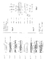
- the whole semiconducting substrate 1 which, as shown, may be constituted by an epitaxial layer of doped silicon having a p-type conductivity, is subjected to thermal oxidation in order to grow a thin layer of so-called "pad" oxide 2 whose thickness may be comprised between 10 and 20 nm and in any case such as to sufficiently protect the semiconducting substrate during the following steps of the process.
- pad oxide 2 whose thickness may be comprised between 10 and 20 nm and in any case such as to sufficiently protect the semiconducting substrate during the following steps of the process.
- a silicon nitride layer 3 is deposited with a thickness of about 150 nm and above the deposited silicon nitride layer 3 a photoresist mask (not shown) is formed for defining the areas where a relatively thick field oxide layer will be grown, i.e.
- a layer of field oxide 4 is thermally grown until it reaches a thickness of about 600 nm.
- the nitride layer constitutes an oxygen impervious mask for growing the field oxide 4.
- a new cycle of thermal oxidation is carried out to form a layer of sacrificial oxide having a thickness which may be comprised between 30 and 50 nm and then it is etched away.
- a partial growth of a gate oxide layer is performed in the cells' area, on the cell areas of the matrix, on the insular areas of the select transistors (cell) as well as of the transistors of the external circuitry (not shown in the figures), for a thickness which, in this first phase of growth, may be comprised between 10 and 20 nm.
- a mask R1 is formed thereafter, the aperture of which is indicated in Fig. 2 by means of the perimeter drawn with a dash line and identified by the arrow and by the label: TUNNEL OXIDE MASK, which masks all the active areas which do not belong to the memory cells of the matrix.
- the gate oxide which was partially grown in the active areas of the memory cells is etched and boron is implanted for modifying in the desired manner the doping level of the channel region of the cells. Therefore this implantation of the active channel area of the matrix's cells is performed in a self alignment manner through slits of the field oxide 4. Boron implantation may be carried out at an energy level of about 60-80 KeV, for a dose of about 4-60 ⁇ 101 atoms/cm. In Figures 2A and 2B this implantation is depicted by the arrows B11.
- the photoresist mask R1 is removed and the wafer is subjected to an oxidation cycle for growing a layer of tunnel oxide on the semiconducting single crystal in the active areas of the matrix's memory cells, from where the partially grown gate oxide layer previously formed had been removed, for a thickness which may be comprised between about 9 and about 12 nm.
- the gate oxide layer which was already partially grown on the active areas of the select transistors and of the transistors of the external circuitry, reaches practically a definitive thickness of about 20 nm.
- a stack composed of: a first deposited layer 7 of polysilicon; an interpoly isolating multilayer, which may be formed by a layer of oxide, a deposited layer of silicon nitride and an oxide layer obtained by oxidizing the deposited nitride and which is commonly known by the acronym ONO (Oxide-Nitride-Oxide), identified as a whole with 8 in the figures and having a total equivalent thickness of about 20 nm; a protective deposited layer 9 of polycrystalline silicon (dummy polysilicon) having a thickness comprised between about 100 and about 150 nm; and finally a deposited layer 10 of silicon nitride having a thickness comprised between 20 and 30 nm.
- ONO Oxide-Nitride-Oxide
- the first layer of polysilicon 7 may be doped in situ by use of POCL3 or by implantation, and from this layer the floating gate of the memory cell as well as the gate structures of the select transistors (SEL) and of the transistors of the external circuitry will be patterned eventually.
- the second layer 9 of polysilicon has the purpose of protecting the thin isolating ONO multilayer 8 during the subsequent steps of the process, while the uppermost layer 10 of silicon nitride has the function of protecting in turn the layer of polysilicon 9 during the subsequent oxidizing treatments.
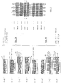
- the process continues with the formation of an R2 mask for defining the first layer of polysilicon and with the etch of the multilayered 6-10 stack and of the field oxide 4.
- the bitlines which intersect the active areas previously defined, by crossing within the memory cell area the horizontal parallel strips which will coincide with the wordlines.
- the bitlines are defined alternately as continuous strips BL and as interrupted strips (BL) (Fig. 4).
- BL' continuous bitlines
- SEL select transistors
- a heavy implantation with an N-type dopant (arsenic and/or phosphorous) is made for forming the diffused bitlines in the p-type semiconducting substrate, as well as the source/drain junctions of the memory cells and of the select transistors (SEL).
- an N-type dopant arsenic and/or phosphorous
- SEL select transistors
- LDD source junctions Lightly Doped Drain extensions
- source-erasable cells i.e. for fabricating FLASH-EPROM memories.
- Such an additional mask is not depicted in the figures but its profile can be easily visualized by a skilled technician.
- phosphorous is implanted in the source areas, which, by virtue of a greater diffusivity as compared to arsenic, will diffuse beyond the diffusion profile of arsenic thus giving to the junction a graduated profile.
- the continous bitlines BL, contacted in metal coincide preferably with the drain areas of the memory cells, while the interrupted bitlines BL', which are contacted through respective select transistors, coincide peferably with the source areas of the memory cells.
- the continuous bitlines BL which are contacted in metal, are made to coincide preferably with the source regions of the cells, while the interrupted bitlines BL', which are contacted through respective select transistors, are made to coincide with the drain regions of the cells. Therefore, the additional mask which is used for effecting the further implantation of the source areas will have a profile such as to mask the interrupted bitlines (BL') and will have openings which projectively superimpose to the continuous bitlines BL.
- the mask used for defining the polysilicon of first level, and which is used also for implanting the bitlines is removed and an oxidation step of the implanted bitlines is performed until growing an oxide layer with a relatively large thickness (from 50 to about 100 nm) over the areas implanted during the preceding step and simultaneously the implanted species diffuse in the semiconducting substrate, as indicated in Figures 5A and 5B.
- the oxide layer 11, grown during this oxidation treatment, will have a thickness which is limited only by the requirement of not excessively diffusing the bitline junction.
- a first planarization step of the surface of the wafers being fabricated is performed by first depositing a layer 12 of planarizing dielectric material and subsequently by etching the deposited layer 12 until exposing the second layer 9 of polysilicon (dummy polysilicon), thus eliminating also the protective layer of silicon nitride 10.
- This planarization step has the purpose not only of facilitating the subsequent masking steps but also of diminishing parasitic capacitive couplings between bitlines and wordlines, by increasing the separation distance therebetween thus overall improving the speed characteristics of the memory.
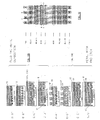
- a M3 mask (MATRIX) is formed, through which mask the second polysilicon layer 9 (dummy polysilicon) and the underlying ONO multilayer 8 are etched off from all the areas outside the area occupied by the matrix of memory cells, and therefore also from the areas of the select transistors (SEL) the area of the external circuitry.
- a boron implantation for threshold adjustment may be effected in the channel areas of the select transistors (SEL) and of the transistors of the external circuitry, in case all these transistors require the same type of implant, otherwise it is possible to use a dedicated mask, THRESHOLD SHIFT MASK, the openings of which are indicated in Fig. 6 by the squares drawn with dash and point line, while the perimeter of said MATRIX mask is indicated in the same Fig. 6 by the perimeter drawn with a dash line.
- Such a boron implantation for adjusting the threshold of select and external circuitry transistors is carried out, as indicated by the arrows in Fig. 6B, through the layer 7 of polysilicon of first level and the underlying gate oxide layer 5.
- the implant conditions may be: energy 50 KeV, dose 1 ⁇ 10 atoms/cm.
- a layer 13 of polysilicon of second level having a thickness of about 100 nm is deposited and doped and thereafter a layer 14 of tungsten silicide having a thickness of about 250 nm is deposited over the polysilicon of second level in order to increase the conductivity of the wordlines of the memory which will be patterned in this conducting stack thus reducing the time constant RC affecting propagation of address signals through the memory matrix.
- a mask M4 for defining the polysilicon of second level is through this mask the gate of the external circuitry and of the select transistors (SEL), as well as the wordlines of the memory cells (control gates) are defined.
- the etching of the polysilicon is arrested eventually either on the field oxide 4 or on the planarization dielectric 12 in peripheral external areas, while in the area occupied by the matrix of memory cells, the etching is arrested on the ONO interpoly dielectric multilayer 8.
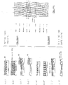
- the process of fabrication proceeds with the formation of a mask M5 for a self-aligned etching pertaining solely to the area occupied by the memory cells, as depicted by the perimeter drawn with a dash line and labelled SELF ALIGNED ETCH MASK of Fig. 8 which identifies an opening of the mask.
- This mask is used for defining and separating the floating gates of single cells aligned along a same column of the matrix.
- the ONO stack 8 and the polysilicon of first level 7 are etched in a selfalignment manner. Etching is arrested on the field oxide 4 thus determining a partial superimposition of the gate structure of the cells over the adjacent edges of the field oxide, for achieving a sufficient capacitive coupling.
- the process of fabrication of the whole integrated circuit may proceed in a standard manner by defining the n-type and p-type junctions of the external circuitry. These further steps of a standard CMOS process do not pertain to the array of memory cells and of the select transistors (SEL) and therefore are not illustrated and described.
- SEL select transistors
- a new cycle of planarization is performed by depositing a layer of planarizing dielectric material 15 and subsequently carrying out a blanket etching step.
- the process proceeds with the deposition of an intermediate dielectric layer 16, with the formation of a contact-opening mask M6 and with the etching of the whole dielectric layer until exposing the silicon in the contact areas (C) of continuous bitlines (BL) (Fig. 9B).
- deposition of metallic plugs 17 in the contact holes and of a metal layer 18 (Fig. 10A) follows.
- a further mask M7 for defining the metal 18 is formed and the metal is etched.
- Fig. 10 depicts the layout of the memory cells.
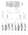
- FIG. 9bis An alternative embodiment of the process of the invention is depicted in the series of Figures starting from Fig. 3bis to Fig. 9bis.
- the fundamental difference between the two embodiments consists in the mask used for defining the polysilicon of the first level, according to which, while in the described first embodiment slits coinciding with the diffused memory bitlines to be formed were defined, according to the following alternative embodiment, parallel strips of polysilicon of first level are defined which will originate the floating gates of the cells.
- the fabrication process according to this alternative embodiment remains identical to the process already described for the first steps until the growth of a tunnel oxide layer with a thickness comprised between 9 and 12 nm. Thereafter, as shown in Figures 3bisB, differently from the process described before, a first layer of polysilicon 7 is deposited and above the deposited layer of polysilicon 7 an interpoly dielectric ONO multilayer 8 is formed.
- a mask R2bis is formed for defining the polysilicon of first level and through this mask the stack 6-8 and the field oxide 4 are also etched. As shown in light field in the plan view of Fig. 4bis, these steps define strips of polysilicon between which the future bitline will be formed, alternately, in a continuous form (BL) and in an interrupted form (BL'). Of course also in this case, the future continuous bitlines BL will be contacted directly in metal through a plurality of spaced contacts which will be formed in the prearranged areas (C(n), C(n+1)),, while the interrupted bitlines BL' will be contacted through respective select transistors (SEL).
- SEL select transistors
- a new mask (not shown in the figures) is formed thereafter for masking the area external to the area occupied by the memory cells and by the select transistors (SEL) for implanting the bitlines with a heavy dose of an n-type dopant (arsenic and/or phosphorous) in order to form bitlines diffused in the p-type semiconducting substrate as well as the source/drain junctions of the memory cells and of the select transistors (SEL).
- This mask was not necessary in the process of the first embodiment and therefore this alternative embodiment will require one additional mask.
- an M3 mask (MATRIX) is formed for removing the dielectric ONO multilayer 8, the polysilicon of first level 7 and the gate oxide layer 5 from the areas of the select transistors (SEL) and of the external circuitry.
- the thickness of the oxide grown on the diffused bitlines is substantially limited to the thickness of the gate oxide typical of the particular CMOS process used.
- a mask M3 is formed for carrying out a threshold adjustment implantation, by implanting boron through the gate oxide which was formed during the preceding step in the channel areas of the select transistors (SEL) and of the transistors of the external circuitry.
- a polysilicon layer of second level 13 is deposited and doped. Thereafter a layer of tungsten silicide 14 is deposited.
- a mask M4 is formed for defining the polysilicon of second level thus defining also the gates of the external circuitry, of the select transistors (SEL) and the wordlines (control gates) of the memory cells.
- the etching of the polysilicon is arrested on the field oxide 4 or on the gate oxide layer 5 grown on the diffused bitlines, except in the area occupied by the memory cells where it is arrested on the ONO multilayer layer 8.
- a mask M5 pertaining only to the area occupied by the memory cells is formed for conducting a self-aligned etching step. Through this mask the floating gates of the individual cells are defined and separated from each other, by etching the ONO layer 8 and the polysilicon of first level 7.
- the fabrication process may then continue according to a standard CMOS sequence.
- N-type and p-type junctions of the external circuitry (not shown in the figures) are defined and implanted, a planarization step is performed and an intermediate dielectric layer 16 is deposited as already described. Similarly, a contact mask M6 is formed and the contacts are opened.
- Figures 9bis, 9bisA and 9bisB the deposition of metallic plugs 17 in the contacts and of the metal layer 18 is shown.
- Fig. 9bisB depicts the formation of the mask M7 for defining the metal and the subsequent etching of the metal layer 18.
- Fig. 9bis shows the layout of the memory cells as produced by this alterantive embodiment of the process of the invention.
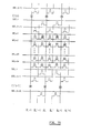
- FIG. 11 A functional diagram of an EPROM memory array which may be fabricated by the process of the invention is depicted in Fig. 11.
- the operation of the memory circuit is similar to that of the memory array described in the cited article: "Alternate Metal Virtual Ground (AMG) - A New Scaling Concept for Very High-Density EPROM's, by Boaz Eitan, IEEE 1991, Vol. 12, No. 8, August 1991", and the content of which is herein incorporated by express reference.
- AMG Alternate Metal Virtual Ground
- the improved fabrication process of the invention employs relatively non-critical masks and permits the fabrication of high density electrically programmable and erasable (EEPROM or FLASH-EPROM) devices.
- EEPROM electrically programmable and erasable
- the novel process permits the fabrication of a contactless type, cross-point cell definition, memory matrix which provides for a more comfortable "pitch" of bitline metal-definition while, on the other hand, realizes cell layout characterized by a gate structure extending laterally over adjacent portions of field oxide, thus establishing an appropriate capacitive coupling between control and floating gates.
Landscapes
- Non-Volatile Memory (AREA)
- Semiconductor Memories (AREA)
Claims (7)
- Procédé de fabrication d'une matrice de cellules mémoire à grille flottante organisée en rangées et colonnes, avec des lignes de bits sous forme de régions diffusées, alternativement- continues et contactées directement par une ligne métallique, et- discontinues et contactées par l'intermédiaire de transistors de sélection respectifs, ces transistors de sélection étant disposés selon au moins deux rangées décalées qui sont prévues à intervalles d'un certain nombre de rangées de cellules de la matrice mémoire,sur un substrat semiconducteur d'un premier type de conductivité et comprenant les étapes suivantes :former une couche d'oxyde de base (2) sur le substrat (1), déposer et définir une couche de nitrure de masquage (3) ;former un oxyde de champ (4) définissant des régions de canal des cellules sous forme de bandes parallèles orientées selon une première direction et des rangées de zones insulaires décalées des transistors de sélection et de contact des lignes de bits continues ;enlever le nitrure de masquage et l'oxyde de base ;faire croître thermiquement une couche d'oxyde de grille (5) ayant une certaine épaisseur partielle sur les régions de canal et les zones insulaires définies par l'oxyde de champ ;définir par masquage la zone de matrice de cellules mémoire, graver l'oxyde de grille et implanter un dopant du premier type de conductivité dans les zones de canal des cellules mémoire, et enlever le masque et faire croître une couche d'oxyde tunnel (6) ayant une épaisseur inférieure à l'épaisseur partielle de la couche d'oxyde de grille enlevée, tout en augmentant l'épaisseur de la couche d'oxyde de grille dans les autres zones ;déposer une couche de silicium polycristallin de premier niveau (7) et doper le silicium polycristallin pour augmenter la conductivité électrique à une valeur désirée, former un multicouche isolant interpoly (8), déposer une couche de protection de silicium polycristallin (9) au-dessus du multicouche isolant interpoly et déposer une couche de nitrure de silicium (10) ayant une épaisseur propre à protéger de l'oxydation la couche protectrice de silicium polycristallin ;masquer la couche de nitrure de silicium ;graver la couche de nitrure de silicium, la couche de silicium polycristallin protectrice, le multicouche isolant interpoly, la couche de silicium polycristallin dopé de premier niveau, l'oxyde de grille ou tunnel et l'oxyde de champ au niveau des croisements jusqu'à exposer le substrat semiconducteur selon une pluralité de bandes alternativement continues et interrompues, parallèles les unes aux autres et orientées orthogonalement aux bandes sous-jacentes d'oxyde de champ définissant les régions de canal en forme de bande, dans la zone occupée par la matrice de cellules ;implanter une dose élevée d'un dopant propre à produire un second type de conductivité dans les zones exposées du substrat semiconducteur à l'intérieur de la zone matricielle pour former des lignes de bits diffusées de la matrice, chacune coïncidant avec les régions de source ou de drain d'un second type de conductivité des cellules mémoire disposées le long d'une même colonne ;diffuser le dopant implanté et oxyder la surface du substrat semiconducteur dans les zones exposées et implantées pendant les étapes précédentes, tout en maintenant les autres zones externes à la zone occupée par les cellules mémoire protégées d'une oxydation par la couche de nitrure de silicium de protection ;planariser la surface en déposant une couche de planarisation (12) en un matériau diélectrique et graver la couche de planarisation, en continuant ainsi la gravure pour enlever la couche de nitrure de silicium et exposer la couche de protection de silicium polycristallin ;masquer la zone occupée par les cellules mémoire et éliminer la couche protectrice de silicium polycristallin et le multicouche isolant interpoly de toutes les zones externes à ladite zone ;implanter un dopant du premier type de conductivité pour régler le seuil dans les zones de canal des transistors de sélection et des transistors de circuits externes à la matrice de cellules mémoire, à travers la couche de silicium polycristallin dopé de premier niveau et la couche d'oxyde de grille ;déposer et doper une couche de silicium polycristallin de second niveau (13) ;déposer une couche de siliciure de tungstène (14) ;masquer la couche de siliciure de tungstène pour définir la grille des transistors des circuits externes ainsi que des transistors de sélection et les grilles de commande de la matrice de cellules mémoire sous forme de bandes parallèles orientées dans la première direction ;graver la couche de siliciure de tungstène et la couche de silicium polycristallin dopé de second niveau, arrêter la gravure sur l'oxyde de champ ou sur le matériau diélectrique de planarisation dans des zones externes à la zone de la matrice de cellules mémoire et sur le multicouche isolant interpoly à l'intérieur de la zone matricielle ;masquer les zones externes à la zone matricielle ;réaliser une gravure auto-alignée du multicouche isolant interpoly et de la couche de silicium polycristallin dopé de premier niveau à l'intérieur de la zone matricielle ;planariser la surface par dépôt d'une couche de matériau diélectrique de planarisation (15) suivi par une gravure et un dépôt d'une couche diélectrique d'isolement intermédiaire (16) ;former une pluralité de contacts sur chacune des lignes de bits continues disposées de façon alternée aux lignes de bits interrompues et déposer et définir des lignes parallèles d'une couche de métallisation (18) sur chacun de la pluralité de contacts des lignes de bits continues.
- Procédé de fabrication d'une matrice de cellules mémoire à grille flottante organisée en rangées et colonnes, avec des lignes de bits sous forme de régions diffusées, alternativement continues et contactées directement par une ligne métallique, et discontinues et contactées par l'intermédiaire de transistors de sélection respectifs disposés selon au moins deux rangées de cellules décalées qui sont prévues à intervalles d'un certain nombre de rangées de cellules de la matrice mémoire, sur un substrat semiconducteur d'un premier type de conductivité et comprenant les étapes suivantes :former une couche d'oxyde de base (2) sur le substrat (1), déposer et définir une couche de nitrure de masquage (3) ;former un oxyde de champ (4) définissant des régions de canal des cellules sous forme de bandes parallèles orientées selon une première direction et de rangées de zones insulaires décalées des transistors de sélection et de contacts des lignes de bits continues ;enlever le nitrure de masquage et l'oxyde de base ; faire croître thermiquement une couche d'oxyde de grille (5) sur les régions de canal et les zones insulaires définies par l'oxyde de champ ;définir par masquage la zone de matrice de cellules mémoire, graver l'oxyde de grille et implanter un dopant du premier type de conductivité dans les zones de canal des cellules mémoire, et enlever le masque et faire croître une couche d'oxyde tunnel (6) ayant une épaisseur inférieure à l'épaisseur de la couche d'oxyde de grille enlevée ;déposer une couche de silicium polycristallin de premier niveau (7) et doper le silicium polycristallin pour augmenter la conductivité électrique à une valeur désirée, former un multicouche isolant interpoly (8) ;masquer le multicouche isolant interpoly ;graver le multicouche isolant interpoly, la couche de silicium polycristallin dopé de premier niveau, l'oxyde de grille ou tunnel, et l'oxyde de champ au niveau des croisements jusqu'à exposer le substrat semiconducteur selon une pluralité de bandes alternativement continues et interrompues, parallèles les unes aux autres et orientées orthogonalement aux bandes sous-jacentes d'oxyde de champ définissant les régions de canal en forme de bande, dans la zone occupée par la matrice de cellules et en laissant des bandes de multicouche isolant interpoly et de silicium polycristallin dopé de premier niveau dans la zone matricielle ;masquer les zones externes à la zone matricielle et implanter une dose élevée d'un dopant propre à produire un second type de conductivité dans les zones exposées du substrat semiconducteur à l'intérieur de la zone matricielle pour former des lignes de bits de la matrice, chacune coïncidant avec les régions de source ou de drain du second type de conductivité des cellules mémoire disposées le long d'une même colonne ;diffuser le dopant implanté et oxyder la surface du substrat semiconducteur dans les zones exposées et implantées pendant les étapes précédentes et former à nouveau une couche d'oxyde de grille dans les zones des transistors de sélection et des circuits externes ;masquer la zone matricielle et graver le multicouche isolant interpoly, le silicium polycristallin dopé de premier niveau et l'oxyde de grille et enlever le masque ;masquer la zone occupée par les cellules mémoire et implanter un dopant du premier type de conductivité pour régler le seuil dans les zones de canal des transistors de sélection et des transistors de circuits externes à la matrice de cellules mémoire, à travers la couche d'oxyde reformée ;déposer et doper une couche de silicium polycristallin de second niveau (13) ;déposer une couche de siliciure de tungstène (14) ;masquer la couche de siliciure de tungstène pour définir la grille des transistors des circuits externes ainsi que des transistors de sélection et les grilles de commande de la matrice de cellules mémoire sous forme de bandes parallèles orientées dans la première direction ;graver la couche de siliciure de tungstène et la couche de silicium polycristallin dopé de second niveau, arrêter la gravure sur l'oxyde de champ dans les zones externes à la zone de la matrice de cellules mémoire et sur le multicouche isolant interpoly à l'intérieur de la zone matricielle ;masquer les zones externes à la zone matricielle ;réaliser une gravure auto-alignée du multicouche isolant interpoly et de la couche de silicium polycristallin dopé de premier niveau à l'intérieur de la zone matricielle ;planariser la surface par dépôt d'une couche de matériau diélectrique de planarisation (15) suivi par une gravure et un dépôt d'une couche diélectrique d'isolement intermédiaire (16) ;former une pluralité de contacts sur chacune des lignes de bits continues disposées de façon alternée aux lignes de bits interrompues et déposer et définir des lignes parallèles d'une couche de métallisation (18) sur chacun de la pluralité de contacts des lignes de bits continues.
- Procédé selon la revendication 1 ou 2, dans lequel le multicouche d'isolement interpoly comprend une couche d'oxyde de silicium obtenue par oxydation du silicium polycristallin, une couche déposée de nitrure de silicium et une couche d'oxyde de silicium obtenue en oxydant une partie de l'épaisseur de la couche déposée de nitrure de silicium.
- Procédé selon la revendication 1 ou 2, dans lequel les lignes de bits continues contactées par une couche de métallisation coïncident avec les régions de drain des cellules mémoire disposées le long d'une même colonne de la matrice et les lignes de bits interrompues contactées par l'intermédiaire de transistors de sélection respectifs coïncident avec les régions de source des cellules mémoire agencées le long d'une même colonne de la matrice.
- Procédé selon la revendication 1 ou 2, dans lequel le substrat semiconducteur est du silicium de type p et le dopant implanté dans les lignes de bits appartient au groupe comprenant l'arsenic et le phosphore.
- Procédé selon la revendication 5, comprenant en outre une étape d'implantation de toutes les lignes de bits de la matrice par de l'arsenic, le masquage de toutes les lignes de bits coïncidant avec les régions de drain des cellules mémoire ;l'implantation de phosphore dans les zones de lignes de bits non-masquées qui coïncident avec les régions de source des cellules mémoire pour former des diffusions de source graduées s'étendant sous le bord de la grille flottante correspondante.
- Procédé selon la revendication 6, dans lequel les lignes de bits qui coïncident avec les régions de drain des cellules mémoires sont des lignes de bits interrompues contactées par l'intermédiaire des transistors de sélection et les lignes de bits qui coïncident avec les régions de source des cellules mémoires sont des lignes de bits continues qui sont en contact avec une couche de métallisation.
Priority Applications (5)
| Application Number | Priority Date | Filing Date | Title |
|---|---|---|---|
| DE69207386T DE69207386T2 (de) | 1992-06-01 | 1992-06-01 | Verfahren zur Herstellung hochintegrierter kontaktloser EPROM's |
| EP92830282A EP0573728B1 (fr) | 1992-06-01 | 1992-06-01 | Procédé de fabrication d'EPROM sans contacts à haute densité d'intégration |
| US08/070,084 US5723350A (en) | 1992-06-01 | 1993-05-28 | Process for fabricating a contactless electrical erasable EPROM memory device |
| JP5156098A JPH06188396A (ja) | 1992-06-01 | 1993-06-01 | 電気的に消去できる無接点epromメモリデバイスの製造方法 |
| US08/458,059 US5707884A (en) | 1992-06-01 | 1995-06-01 | Process for fabricating a contactless electrical erasable EPROM memory device |
Applications Claiming Priority (1)
| Application Number | Priority Date | Filing Date | Title |
|---|---|---|---|
| EP92830282A EP0573728B1 (fr) | 1992-06-01 | 1992-06-01 | Procédé de fabrication d'EPROM sans contacts à haute densité d'intégration |
Publications (2)
| Publication Number | Publication Date |
|---|---|
| EP0573728A1 EP0573728A1 (fr) | 1993-12-15 |
| EP0573728B1 true EP0573728B1 (fr) | 1996-01-03 |
Family
ID=8212118
Family Applications (1)
| Application Number | Title | Priority Date | Filing Date |
|---|---|---|---|
| EP92830282A Expired - Lifetime EP0573728B1 (fr) | 1992-06-01 | 1992-06-01 | Procédé de fabrication d'EPROM sans contacts à haute densité d'intégration |
Country Status (4)
| Country | Link |
|---|---|
| US (2) | US5723350A (fr) |
| EP (1) | EP0573728B1 (fr) |
| JP (1) | JPH06188396A (fr) |
| DE (1) | DE69207386T2 (fr) |
Cited By (1)
| Publication number | Priority date | Publication date | Assignee | Title |
|---|---|---|---|---|
| US6251736B1 (en) | 1998-12-29 | 2001-06-26 | Stmicroelectronics S.R.L. | Method for forming contactless MOS transistors and resulting devices, especially for use in non-volatile memory arrays |
Families Citing this family (18)
| Publication number | Priority date | Publication date | Assignee | Title |
|---|---|---|---|---|
| US5604141A (en) * | 1994-03-15 | 1997-02-18 | National Semiconductor Corporation | Method for forming virtual-ground flash EPROM array with reduced cell pitch in the X direction |
| US5409854A (en) * | 1994-03-15 | 1995-04-25 | National Semiconductor Corporation | Method for forming a virtual-ground flash EPROM array with floating gates that are self aligned to the field oxide regions of the array |
| US5436478A (en) * | 1994-03-16 | 1995-07-25 | National Semiconductor Corporation | Fast access AMG EPROM with segment select transistors which have an increased width |
| DE69738971D1 (de) * | 1996-06-28 | 2008-10-23 | Texas Instruments Inc | Wortleitungsanordnung für Halbleiter-Speicherbauteil |
| EP0851485B1 (fr) * | 1996-12-24 | 2007-05-23 | STMicroelectronics S.r.l. | Procédé de gravure auto-alignée pour la réalisation des lignes de mot des dispositifs de mémoire intégrée semi-conductrice |
| DE69636738D1 (de) * | 1996-12-27 | 2007-01-11 | St Microelectronics Srl | Kontaktstruktur für elektronische EPROM oder flash EPROM Halbleiterschaltungen und ihr Herstellungsverfahren |
| US6013551A (en) * | 1997-09-26 | 2000-01-11 | Taiwan Semiconductor Manufacturing Company, Ltd. | Method of manufacture of self-aligned floating gate, flash memory cell and device manufactured thereby |
| KR100277888B1 (ko) * | 1997-12-31 | 2001-02-01 | 김영환 | 플래쉬메모리및그의제조방법 |
| JPH11265987A (ja) * | 1998-01-16 | 1999-09-28 | Oki Electric Ind Co Ltd | 不揮発性メモリ及びその製造方法 |
| ITTO980516A1 (it) * | 1998-06-12 | 1999-12-12 | St Microelectronics Srl | Procedimento per la fabbricazione di transistori di selezione di memor ie non volatili serial-flash, eprom, eeprom e flash-eeprom in configur |
| US6033955A (en) * | 1998-09-23 | 2000-03-07 | Advanced Micro Devices, Inc. | Method of making flexibly partitioned metal line segments for a simultaneous operation flash memory device with a flexible bank partition architecture |
| EP1032035B1 (fr) * | 1999-02-26 | 2004-10-13 | STMicroelectronics S.r.l. | Procédé de fabrication de dispositifs électroniques de mémoire avec matrice de cellules à masse virtuelle |
| EP1032029A1 (fr) | 1999-02-26 | 2000-08-30 | STMicroelectronics S.r.l. | Procédé de fabrication de dispositifs intégrés à semi-conducteur de mémoire électronique ayant une matrice de cellules à masse virtuelle |
| US7064978B2 (en) * | 2002-07-05 | 2006-06-20 | Aplus Flash Technology, Inc. | Monolithic, combo nonvolatile memory allowing byte, page and block write with no disturb and divided-well in the cell array using a unified cell structure and technology with a new scheme of decoder and layout |
| US6862223B1 (en) * | 2002-07-05 | 2005-03-01 | Aplus Flash Technology, Inc. | Monolithic, combo nonvolatile memory allowing byte, page and block write with no disturb and divided-well in the cell array using a unified cell structure and technology with a new scheme of decoder and layout |
| KR100655287B1 (ko) * | 2004-11-11 | 2006-12-11 | 삼성전자주식회사 | 플로팅 게이트를 갖는 비휘발성 기억 소자의 형성 방법 |
| KR100944591B1 (ko) * | 2007-12-03 | 2010-02-25 | 주식회사 동부하이텍 | 반도체 소자 및 그 제조 방법 |
| US8859343B2 (en) * | 2013-03-13 | 2014-10-14 | Macronix International Co., Ltd. | 3D semiconductor structure and manufacturing method thereof |
Family Cites Families (23)
| Publication number | Priority date | Publication date | Assignee | Title |
|---|---|---|---|---|
| US4519849A (en) * | 1980-10-14 | 1985-05-28 | Intel Corporation | Method of making EPROM cell with reduced programming voltage |
| US4597060A (en) * | 1985-05-01 | 1986-06-24 | Texas Instruments Incorporated | EPROM array and method for fabricating |
| US4892840A (en) * | 1986-03-27 | 1990-01-09 | Texas Instruments Incorporated | EPROM with increased floating gate/control gate coupling |
| US4785375A (en) * | 1987-06-11 | 1988-11-15 | Tam Ceramics, Inc. | Temperature stable dielectric composition at high and low frequencies |
| US4780424A (en) * | 1987-09-28 | 1988-10-25 | Intel Corporation | Process for fabricating electrically alterable floating gate memory devices |
| US4951103A (en) * | 1988-06-03 | 1990-08-21 | Texas Instruments, Incorporated | Fast, trench isolated, planar flash EEPROMS with silicided bitlines |
| US4996668A (en) * | 1988-08-09 | 1991-02-26 | Texas Instruments Incorporated | Erasable programmable memory |
| US5110753A (en) * | 1988-11-10 | 1992-05-05 | Texas Instruments Incorporated | Cross-point contact-free floating-gate memory array with silicided buried bitlines |
| US5051796A (en) * | 1988-11-10 | 1991-09-24 | Texas Instruments Incorporated | Cross-point contact-free array with a high-density floating-gate structure |
| IT1235690B (it) * | 1989-04-07 | 1992-09-21 | Sgs Thomson Microelectronics | Procedimento di fabbricazione per una matrice di celle eprom organizzate a tovaglia. |
| US4939105A (en) * | 1989-08-03 | 1990-07-03 | Micron Technology, Inc. | Planarizing contact etch |
| JPH0783066B2 (ja) * | 1989-08-11 | 1995-09-06 | 株式会社東芝 | 半導体装置の製造方法 |
| IT1236601B (it) * | 1989-12-22 | 1993-03-18 | Sgs Thomson Microelectronics | Dispositivo a semiconduttore integrato di tipo eprom con connessioni metalliche di source e procedimento per la sua fabbricazione. |
| US5111270A (en) * | 1990-02-22 | 1992-05-05 | Intel Corporation | Three-dimensional contactless non-volatile memory cell |
| US5087584A (en) * | 1990-04-30 | 1992-02-11 | Intel Corporation | Process for fabricating a contactless floating gate memory array utilizing wordline trench vias |
| US5071782A (en) * | 1990-06-28 | 1991-12-10 | Texas Instruments Incorporated | Vertical memory cell array and method of fabrication |
| US5077230A (en) * | 1990-08-03 | 1991-12-31 | Intel Corporation | Method for improving erase characteristics of buried bit line flash EPROM devices by use of a thin nitride layer formed during field oxide growth |
| US5075245A (en) * | 1990-08-03 | 1991-12-24 | Intel Corporation | Method for improving erase characteristics of buried bit line flash EPROM devices without using sacrificial oxide growth and removal steps |
| US5102814A (en) * | 1990-11-02 | 1992-04-07 | Intel Corporation | Method for improving device scalability of buried bit line flash EPROM devices having short reoxidation beaks and shallower junctions |
| US5212541A (en) * | 1991-04-18 | 1993-05-18 | National Semiconductor Corporation | Contactless, 5v, high speed eprom/flash eprom array utilizing cells programmed using source side injection |
| US5120670A (en) * | 1991-04-18 | 1992-06-09 | National Semiconductor Corporation | Thermal process for implementing the planarization inherent to stacked etch in virtual ground EPROM memories |
| US5240870A (en) * | 1991-04-18 | 1993-08-31 | National Semiconductor Corporation | Stacked gate process flow for cross-point EPROM with internal access transistor |
| US5346842A (en) * | 1992-02-04 | 1994-09-13 | National Semiconductor Corporation | Method of making alternate metal/source virtual ground flash EPROM cell array |
-
1992
- 1992-06-01 DE DE69207386T patent/DE69207386T2/de not_active Expired - Fee Related
- 1992-06-01 EP EP92830282A patent/EP0573728B1/fr not_active Expired - Lifetime
-
1993
- 1993-05-28 US US08/070,084 patent/US5723350A/en not_active Expired - Lifetime
- 1993-06-01 JP JP5156098A patent/JPH06188396A/ja active Pending
-
1995
- 1995-06-01 US US08/458,059 patent/US5707884A/en not_active Expired - Lifetime
Cited By (1)
| Publication number | Priority date | Publication date | Assignee | Title |
|---|---|---|---|---|
| US6251736B1 (en) | 1998-12-29 | 2001-06-26 | Stmicroelectronics S.R.L. | Method for forming contactless MOS transistors and resulting devices, especially for use in non-volatile memory arrays |
Also Published As
| Publication number | Publication date |
|---|---|
| JPH06188396A (ja) | 1994-07-08 |
| US5723350A (en) | 1998-03-03 |
| DE69207386T2 (de) | 1996-09-12 |
| DE69207386D1 (de) | 1996-02-15 |
| US5707884A (en) | 1998-01-13 |
| EP0573728A1 (fr) | 1993-12-15 |
Similar Documents
| Publication | Publication Date | Title |
|---|---|---|
| US5707884A (en) | Process for fabricating a contactless electrical erasable EPROM memory device | |
| US5168334A (en) | Non-volatile semiconductor memory | |
| US5049515A (en) | Method of making a three-dimensional memory cell with integral select transistor | |
| US5966603A (en) | NROM fabrication method with a periphery portion | |
| US5021848A (en) | Electrically-erasable and electrically-programmable memory storage devices with self aligned tunnel dielectric area and the method of fabricating thereof | |
| US4804637A (en) | EEPROM memory cell and driving circuitry | |
| US6709922B2 (en) | Method of manufacturing semiconductor integrated circuit device including nonvolatile semiconductor memory devices | |
| US5768186A (en) | High density single poly metal-gate non-volatile memory cell | |
| US5270240A (en) | Four poly EPROM process and structure comprising a conductive source line structure and self-aligned polycrystalline silicon digit lines | |
| US5284785A (en) | Diffusionless source/drain conductor electrically-erasable, electrically-programmable read-only memory and methods for making and using the same | |
| US5019879A (en) | Electrically-flash-erasable and electrically-programmable memory storage devices with self aligned tunnel dielectric area | |
| US4780424A (en) | Process for fabricating electrically alterable floating gate memory devices | |
| EP0085551A2 (fr) | Procédé de fabrication d'une matrice de mémoires du type MOS comprenant des éléments de stockage électriquement programmables et électriquement effaçables | |
| EP0780902A1 (fr) | Mémoire rémanente semi-conductrice et méthode de fabrication | |
| US5149665A (en) | Conductive source line for high density programmable read-only memory applications | |
| US5350706A (en) | CMOS memory cell array | |
| EP0422606B1 (fr) | Dispositif semi-conducteur comprenant des E2PROM et des EPROM dans une puce | |
| JPH08298295A (ja) | 不揮発性半導体記憶装置及びその製造方法 | |
| US5385856A (en) | Manufacture of the fieldless split-gate EPROM/Flash EPROM | |
| US6037226A (en) | Method of making contactless nonvolatile semiconductor memory with asymmetrical floating gate | |
| US5466624A (en) | Isolation between diffusion lines in a memory array | |
| US5238855A (en) | Cross-point contact-free array with a high-density floating-gate structure | |
| US6359305B1 (en) | Trench-isolated EEPROM flash in segmented bit line page architecture | |
| JPH06283721A (ja) | 不揮発性メモリ・セル、アレー装置、製造方法、及びそのメモリ回路 | |
| US5340768A (en) | Method of fabricating self-aligned field-plate isolation between control electrodes |
Legal Events
| Date | Code | Title | Description |
|---|---|---|---|
| PUAI | Public reference made under article 153(3) epc to a published international application that has entered the european phase |
Free format text: ORIGINAL CODE: 0009012 |
|
| AK | Designated contracting states |
Kind code of ref document: A1 Designated state(s): DE FR GB IT SE |
|
| 17P | Request for examination filed |
Effective date: 19940520 |
|
| 17Q | First examination report despatched |
Effective date: 19950421 |
|
| GRAA | (expected) grant |
Free format text: ORIGINAL CODE: 0009210 |
|
| AK | Designated contracting states |
Kind code of ref document: B1 Designated state(s): DE FR GB IT SE |
|
| REF | Corresponds to: |
Ref document number: 69207386 Country of ref document: DE Date of ref document: 19960215 |
|
| ITF | It: translation for a ep patent filed | ||
| PG25 | Lapsed in a contracting state [announced via postgrant information from national office to epo] |
Ref country code: SE Effective date: 19960403 |
|
| ET | Fr: translation filed | ||
| PLBE | No opposition filed within time limit |
Free format text: ORIGINAL CODE: 0009261 |
|
| 26N | No opposition filed | ||
| REG | Reference to a national code |
Ref country code: GB Ref legal event code: IF02 |
|
| PGFP | Annual fee paid to national office [announced via postgrant information from national office to epo] |
Ref country code: DE Payment date: 20020610 Year of fee payment: 11 |
|
| PG25 | Lapsed in a contracting state [announced via postgrant information from national office to epo] |
Ref country code: DE Free format text: LAPSE BECAUSE OF NON-PAYMENT OF DUE FEES Effective date: 20040101 |
|
| PGFP | Annual fee paid to national office [announced via postgrant information from national office to epo] |
Ref country code: GB Payment date: 20040526 Year of fee payment: 13 |
|
| PGFP | Annual fee paid to national office [announced via postgrant information from national office to epo] |
Ref country code: FR Payment date: 20040608 Year of fee payment: 13 |
|
| PG25 | Lapsed in a contracting state [announced via postgrant information from national office to epo] |
Ref country code: IT Free format text: LAPSE BECAUSE OF NON-PAYMENT OF DUE FEES;WARNING: LAPSES OF ITALIAN PATENTS WITH EFFECTIVE DATE BEFORE 2007 MAY HAVE OCCURRED AT ANY TIME BEFORE 2007. THE CORRECT EFFECTIVE DATE MAY BE DIFFERENT FROM THE ONE RECORDED. Effective date: 20050601 Ref country code: GB Free format text: LAPSE BECAUSE OF NON-PAYMENT OF DUE FEES Effective date: 20050601 |
|
| PG25 | Lapsed in a contracting state [announced via postgrant information from national office to epo] |
Ref country code: FR Free format text: LAPSE BECAUSE OF NON-PAYMENT OF DUE FEES Effective date: 20060228 |
|
| GBPC | Gb: european patent ceased through non-payment of renewal fee |
Effective date: 20050601 |
|
| REG | Reference to a national code |
Ref country code: FR Ref legal event code: ST Effective date: 20060228 |