EP0573911B1 - Procédé de dépôt de couches d'oxyde de silicium à caractéristiques améliorées - Google Patents
Procédé de dépôt de couches d'oxyde de silicium à caractéristiques améliorées Download PDFInfo
- Publication number
- EP0573911B1 EP0573911B1 EP93109008A EP93109008A EP0573911B1 EP 0573911 B1 EP0573911 B1 EP 0573911B1 EP 93109008 A EP93109008 A EP 93109008A EP 93109008 A EP93109008 A EP 93109008A EP 0573911 B1 EP0573911 B1 EP 0573911B1
- Authority
- EP
- European Patent Office
- Prior art keywords
- silicon oxide
- nitrogen
- carried out
- deposition
- teos
- Prior art date
- Legal status (The legal status is an assumption and is not a legal conclusion. Google has not performed a legal analysis and makes no representation as to the accuracy of the status listed.)
- Expired - Lifetime
Links
Images

Classifications
-
- H—ELECTRICITY
- H10—SEMICONDUCTOR DEVICES; ELECTRIC SOLID-STATE DEVICES NOT OTHERWISE PROVIDED FOR
- H10P—GENERIC PROCESSES OR APPARATUS FOR THE MANUFACTURE OR TREATMENT OF DEVICES COVERED BY CLASS H10
- H10P14/00—Formation of materials, e.g. in the shape of layers or pillars
- H10P14/60—Formation of materials, e.g. in the shape of layers or pillars of insulating materials
-
- H—ELECTRICITY
- H10—SEMICONDUCTOR DEVICES; ELECTRIC SOLID-STATE DEVICES NOT OTHERWISE PROVIDED FOR
- H10P—GENERIC PROCESSES OR APPARATUS FOR THE MANUFACTURE OR TREATMENT OF DEVICES COVERED BY CLASS H10
- H10P14/00—Formation of materials, e.g. in the shape of layers or pillars
- H10P14/60—Formation of materials, e.g. in the shape of layers or pillars of insulating materials
- H10P14/69—Inorganic materials
- H10P14/692—Inorganic materials composed of oxides, glassy oxides or oxide-based glasses
- H10P14/6921—Inorganic materials composed of oxides, glassy oxides or oxide-based glasses containing silicon
- H10P14/69215—Inorganic materials composed of oxides, glassy oxides or oxide-based glasses containing silicon the material being a silicon oxide, e.g. SiO2
-
- C—CHEMISTRY; METALLURGY
- C23—COATING METALLIC MATERIAL; COATING MATERIAL WITH METALLIC MATERIAL; CHEMICAL SURFACE TREATMENT; DIFFUSION TREATMENT OF METALLIC MATERIAL; COATING BY VACUUM EVAPORATION, BY SPUTTERING, BY ION IMPLANTATION OR BY CHEMICAL VAPOUR DEPOSITION, IN GENERAL; INHIBITING CORROSION OF METALLIC MATERIAL OR INCRUSTATION IN GENERAL
- C23C—COATING METALLIC MATERIAL; COATING MATERIAL WITH METALLIC MATERIAL; SURFACE TREATMENT OF METALLIC MATERIAL BY DIFFUSION INTO THE SURFACE, BY CHEMICAL CONVERSION OR SUBSTITUTION; COATING BY VACUUM EVAPORATION, BY SPUTTERING, BY ION IMPLANTATION OR BY CHEMICAL VAPOUR DEPOSITION, IN GENERAL
- C23C16/00—Chemical coating by decomposition of gaseous compounds, without leaving reaction products of surface material in the coating, i.e. chemical vapour deposition [CVD] processes
- C23C16/22—Chemical coating by decomposition of gaseous compounds, without leaving reaction products of surface material in the coating, i.e. chemical vapour deposition [CVD] processes characterised by the deposition of inorganic material, other than metallic material
- C23C16/30—Deposition of compounds, mixtures or solid solutions, e.g. borides, carbides, nitrides
- C23C16/40—Oxides
- C23C16/401—Oxides containing silicon
- C23C16/402—Silicon dioxide
-
- C—CHEMISTRY; METALLURGY
- C23—COATING METALLIC MATERIAL; COATING MATERIAL WITH METALLIC MATERIAL; CHEMICAL SURFACE TREATMENT; DIFFUSION TREATMENT OF METALLIC MATERIAL; COATING BY VACUUM EVAPORATION, BY SPUTTERING, BY ION IMPLANTATION OR BY CHEMICAL VAPOUR DEPOSITION, IN GENERAL; INHIBITING CORROSION OF METALLIC MATERIAL OR INCRUSTATION IN GENERAL
- C23C—COATING METALLIC MATERIAL; COATING MATERIAL WITH METALLIC MATERIAL; SURFACE TREATMENT OF METALLIC MATERIAL BY DIFFUSION INTO THE SURFACE, BY CHEMICAL CONVERSION OR SUBSTITUTION; COATING BY VACUUM EVAPORATION, BY SPUTTERING, BY ION IMPLANTATION OR BY CHEMICAL VAPOUR DEPOSITION, IN GENERAL
- C23C16/00—Chemical coating by decomposition of gaseous compounds, without leaving reaction products of surface material in the coating, i.e. chemical vapour deposition [CVD] processes
- C23C16/44—Chemical coating by decomposition of gaseous compounds, without leaving reaction products of surface material in the coating, i.e. chemical vapour deposition [CVD] processes characterised by the method of coating
- C23C16/448—Chemical coating by decomposition of gaseous compounds, without leaving reaction products of surface material in the coating, i.e. chemical vapour deposition [CVD] processes characterised by the method of coating characterised by the method used for generating reactive gas streams, e.g. by evaporation or sublimation of precursor materials
- C23C16/452—Chemical coating by decomposition of gaseous compounds, without leaving reaction products of surface material in the coating, i.e. chemical vapour deposition [CVD] processes characterised by the method of coating characterised by the method used for generating reactive gas streams, e.g. by evaporation or sublimation of precursor materials by activating reactive gas streams before their introduction into the reaction chamber, e.g. by ionisation or addition of reactive species
-
- H—ELECTRICITY
- H10—SEMICONDUCTOR DEVICES; ELECTRIC SOLID-STATE DEVICES NOT OTHERWISE PROVIDED FOR
- H10P—GENERIC PROCESSES OR APPARATUS FOR THE MANUFACTURE OR TREATMENT OF DEVICES COVERED BY CLASS H10
- H10P14/00—Formation of materials, e.g. in the shape of layers or pillars
- H10P14/60—Formation of materials, e.g. in the shape of layers or pillars of insulating materials
- H10P14/63—Formation of materials, e.g. in the shape of layers or pillars of insulating materials characterised by the formation processes
- H10P14/6326—Deposition processes
- H10P14/6328—Deposition from the gas or vapour phase
- H10P14/6334—Deposition from the gas or vapour phase using decomposition or reaction of gaseous or vapour phase compounds, i.e. chemical vapour deposition
-
- H—ELECTRICITY
- H10—SEMICONDUCTOR DEVICES; ELECTRIC SOLID-STATE DEVICES NOT OTHERWISE PROVIDED FOR
- H10P—GENERIC PROCESSES OR APPARATUS FOR THE MANUFACTURE OR TREATMENT OF DEVICES COVERED BY CLASS H10
- H10P14/00—Formation of materials, e.g. in the shape of layers or pillars
- H10P14/60—Formation of materials, e.g. in the shape of layers or pillars of insulating materials
- H10P14/65—Formation of materials, e.g. in the shape of layers or pillars of insulating materials characterised by treatments performed before or after the formation of the materials
- H10P14/6502—Formation of materials, e.g. in the shape of layers or pillars of insulating materials characterised by treatments performed before or after the formation of the materials of treatments performed before formation of the materials
- H10P14/6506—Formation of intermediate materials
-
- H—ELECTRICITY
- H10—SEMICONDUCTOR DEVICES; ELECTRIC SOLID-STATE DEVICES NOT OTHERWISE PROVIDED FOR
- H10P—GENERIC PROCESSES OR APPARATUS FOR THE MANUFACTURE OR TREATMENT OF DEVICES COVERED BY CLASS H10
- H10P14/00—Formation of materials, e.g. in the shape of layers or pillars
- H10P14/60—Formation of materials, e.g. in the shape of layers or pillars of insulating materials
- H10P14/63—Formation of materials, e.g. in the shape of layers or pillars of insulating materials characterised by the formation processes
- H10P14/6326—Deposition processes
- H10P14/6328—Deposition from the gas or vapour phase
- H10P14/6334—Deposition from the gas or vapour phase using decomposition or reaction of gaseous or vapour phase compounds, i.e. chemical vapour deposition
- H10P14/6336—Deposition from the gas or vapour phase using decomposition or reaction of gaseous or vapour phase compounds, i.e. chemical vapour deposition in the presence of a plasma [PECVD]
-
- H—ELECTRICITY
- H10—SEMICONDUCTOR DEVICES; ELECTRIC SOLID-STATE DEVICES NOT OTHERWISE PROVIDED FOR
- H10P—GENERIC PROCESSES OR APPARATUS FOR THE MANUFACTURE OR TREATMENT OF DEVICES COVERED BY CLASS H10
- H10P14/00—Formation of materials, e.g. in the shape of layers or pillars
- H10P14/60—Formation of materials, e.g. in the shape of layers or pillars of insulating materials
- H10P14/66—Formation of materials, e.g. in the shape of layers or pillars of insulating materials characterised by the type of materials
- H10P14/668—Formation of materials, e.g. in the shape of layers or pillars of insulating materials characterised by the type of materials the materials being characterised by the deposition precursor materials
- H10P14/6681—Formation of materials, e.g. in the shape of layers or pillars of insulating materials characterised by the type of materials the materials being characterised by the deposition precursor materials the precursor containing a compound comprising Si
- H10P14/6682—Formation of materials, e.g. in the shape of layers or pillars of insulating materials characterised by the type of materials the materials being characterised by the deposition precursor materials the precursor containing a compound comprising Si the compound being a silane, e.g. disilane, methylsilane or chlorosilane
-
- H—ELECTRICITY
- H10—SEMICONDUCTOR DEVICES; ELECTRIC SOLID-STATE DEVICES NOT OTHERWISE PROVIDED FOR
- H10P—GENERIC PROCESSES OR APPARATUS FOR THE MANUFACTURE OR TREATMENT OF DEVICES COVERED BY CLASS H10
- H10P14/00—Formation of materials, e.g. in the shape of layers or pillars
- H10P14/60—Formation of materials, e.g. in the shape of layers or pillars of insulating materials
- H10P14/69—Inorganic materials
- H10P14/694—Inorganic materials composed of nitrides
- H10P14/6943—Inorganic materials composed of nitrides containing silicon
- H10P14/69433—Inorganic materials composed of nitrides containing silicon the material being a silicon nitride not containing oxygen, e.g. SixNy or SixByNz
Definitions
- This invention relates to an improved method of depositing silicon oxide. More particularly, this invention relates to an improved method of depositing silicon oxide layers on a substrate by thermal decomposition of tetraethoxysilane and ozone.
- multilevel interconnects are made to increase the packing density of devices on a wafer.
- This also requires multilevel dielectric layers to be deposited between conductive layers.
- Such dielectric layers must have good step coverage and planarization properties to produce void-free layers that not only completely fill steps and openings in the underlying substrate, but also form smooth, planarized dielectric layers. Further, such dielectric layers must be able to be deposited at low temperatures, preferably below about 400°C, to avoid damage to underlying, already formed interconnects.
- silicon oxide dielectric layers can be deposited with good conformality and planarization using tetraethoxysilane (hereinafter TEOS), ozone and oxygen at comparatively low temperatures, e.g., about 375°C.
- TEOS tetraethoxysilane
- ozone oxygen
- oxygen e.g., about 375°C.
- the ratio of TEOS and ozone affects the film quality and deposition rate. For example, when depositing silicon oxide from TEOS and ozone using a high ozone:TEOS flow ratio, the rate of deposition is reduced, but the film quality is higher and conformality, i.e., the ability to produce void-free filling and planarized layers, is also higher.
- the layers provide good step coverage and good conformality which leads to excellent planarization, and excellent quality of the silicon oxide when deposited onto silicon.
- the silicon oxide is deposited onto silicon oxide, for example a thermally grown silicon oxide layer
- differences in film quality have arisen.
- the deposition rate of low temperature silicon oxide films from TEOS and ozone deposited onto thermal silicon oxide is about 20% lower, and the wet etch rate of silicon oxide is high, which is indicative of poor quality films.
- the surface of the silicon oxide is very rough and contains voids, indicative of a porous film.
- Fujino et al (Proceedings 7th Int. IEEE VLSI Multilevel Interconnection Conference, June 1990, Santa Clara, C have addressed this problem. Their solution is a two step deposition process; first a deposit of silicon oxide using a low ozone concentration (0.5%) is put down, and a second layer deposited thereover using a high ozone concentration (5%). The result is said to be improved film quality of silicon oxide planarizing films.
- this ozone-TEOS process still has limitations in terms of poor surface quality and surface sensitivity.
- the higher the ozone:TEOS ratio the greater the decrease in oxide deposition rate, and the greater the degradation in film properties, such as wet etch rate, water resistance and stress drift with time.
- the object of the invention is solved by a method of depositing silicon oxide from TEOS and ozone which comprises depositing a first seed layer of a nitrogen-doped PECVD TEOS silicon oxide and depositing a second layer of silicon oxide thereover in a non-plasma, thermal process using high pressure, high ozone:TEOS flow ratios as set forth in claim 1.
- the resultant silicon oxide layers have reduced surface sensitivity and excellent film qualities, and improved conformality of silicon oxide films which can produce void-free films over submicron sized topography.
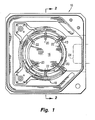
- Figures 1 and 2 are a top plan view and a vertical cross sectional view respectively of a reactor suitable for carrying out the present process.
- the silicon oxide layers deposited in accordance with the invention reduce or eliminate the surface sensitivity problem and the present process provides improved conformality and void-free gap filling capability to silicon oxide films, independent of the type of substrate on which the silicon oxide is deposited.
- Nitrogen atoms can be introduced into the PECVD TEOS silicon oxide underlayers in several ways; for example, nitrogen gas can be added to the standard PECVD TEOS-oxygen process; ammonia (NH 3 ) gas can also be added, either alone or in combination with nitrogen; various oxides of nitrogen including one or more of nitrous oxide (N 2 O), nitric oxide (NO) or nitrogen dioxide (NO 2 ) can be added to the standard TEOS/oxygen process; alternatively, nitrogen, a combination of nitrogen and ammonia, or a combination of one or more nitrogen oxides and ammonia can be added to the reaction in place of part of the free oxygen; or a combination of nitrogen, ammonia and a nitrogen oxide can replace the oxygen in the standard process.
- nitrogen gas can be added to the standard PECVD TEOS-oxygen process
- ammonia (NH 3 ) gas can also be added, either alone or in combination with nitrogen
- a second layer of silicon oxide is deposited over the nitrogen-containing silicon oxide seed layer by known CVD TEOS/ozone/oxygen processes.
- a conventional ozone generator is used to supply a mixture of about 5-13% by weight of ozone in oxygen. This process takes place at comparatively low temperatures of about 350-450°C, which avoids damaging underlying metallization and devices already processed onto the substrate.
- the silicon oxide layer so obtained is highly conformal, and void-free planarizing layers have been deposited onto steps down to about 0.5 ⁇ m in size and aspect ratio of over 1.5:1 using our two layer process.
- the nitrogen-containing films and the ozone TEOS oxides can be deposited in the same reactor, or deposition can take place sequentially in two separate reactors. If two separate reactors are employed, suitably a multichamber apparatus is employed that can deposit sequential layers in two deposition reactors interconnected so that the substrates remain in a vacuum environment. However, exposure of the nitrogen-containing seed layer film to ambient conditions does not affect the ability of the nitrogen-containing seed layers to passivate surface sensitive substrates and to eliminate the surface sensitivity problem.
- a suitable CVD/PECVD reactor in which the present process can be carried out is described in US-A-4,872,947 to Chang et al assigned to Applied Materials, Inc., the assignee of the present invention.
- a top plan view and a vertical cross sectional view of a suitable reactor are shown in Figs. 1 and 2.
- a reactor system 10 comprises a vessel 12 that defines an inner vacuum chamber 13 that has a plasma processing region 14.
- the reactor system 10 also includes a susceptor 16 for holding the substrate and a substrate transport system 18 that includes vertically movable substrate support fingers 20 and susceptor support fingers 22. These fingers cooperate with an external robotic blade 24 for introducing substrates 15 into the chamber 13 and depositing the substrates 15 on the susceptor 16 for processing, and thereafter removing the substrates 15 from the susceptor 16 and the chamber 13.
- the reactor system 10 further comprises a process/purge gas manifold 26 that applies process gas and purging gas to the chamber 13; a high frequency RF power supply and matching network 28, and a low frequency RF power supply and matching network 29 for creating and sustaining a process gas plasma from the inlet gas; and a lamp heating system 30 for heating the susceptor 16 and substrate 15 positioned on the susceptor 16 to effect deposition onto the substrate 15.
- High frequency RF power 13.56 MHz
- lower RF frequencies 100-450 KHz
- a mixture of high and low frequencies can be used to generate a plasma from the process gases.
- a gas manifold 26 supplies process gases to the chamber 13.
- the gas manifold 26 distributes the process gases evenly radially outward across the substrate 15 to promote even deposition across the substrate 15, and can include a RF/gas feed-through device 36 that supplies process gas to the gas manifold 26 that is RF driven. This ensures a high degree of plasma confinement between the manifold 26 and the substrate 15, situate on the susceptor 16 which is grounded.
- a radiant heating system comprises an array of vertically oriented quartz-tungsten-halogen lamps 38 outside the chamber 13 which provide radiant heat to the susceptor 16 and the substrate 15 through a quartz window 40 in the chamber 13. Further details of the PECVD reactor are given in US-A-4,872,947. Deposition of silicon oxide films containing nitrogen can be deposited using standard high frequency RF power, or a mixed high/low frequency RF power can be used.
- the thermal silicon oxide deposition can also be carried out in the same reactor by changing reaction conditions and turning off the RF power to the manifold, or this second deposition step can be carried out in a separate conventional CVD reactor.
- the two reactors can be part of a multichamber reactor in which a central load lock chamber communicates with two or more deposition reactors, carrying out sequential deposition steps without breaking vacuum.
- Such multichamber reactors are commercially available.
- the first nitrogen-containing silicon oxide deposition step is carried out in a PECVD reactor, and the second thermal CVD silicon oxide is carried out in a separate reactor, exposure of the nitrogen-containing silicon oxide film to the ambient will not adversely affect the thermal silicon oxide deposition, and the improved properties and conformality of the second silicon oxide layer are not adversely affected.
- This example illustrates the differences in silicon oxide deposition rate with varying deposition surfaces and with the frequency of the RF source of the plasma in the deposition chamber.
- the first nitrogen-containing silicon oxide layers deposited as above were covered with a thermal CVD silicon oxide layer using a standard TEOS/ozone/oxygen process under the following conditions: Temperature 350-450°C Pressure 66650 Pa (500 Torr-atmospheric pressure) Spacing between gas manifold and substrate 5.08-7.63 mm (200-300 mils) He/TEOS flow 1000-5000 sccm Ozone flow 1000-6000 sccm Ozone concentration 5-13 % (in O 2 )
- Substrate A is silicon
- Substrate B is PECVD TEOS silicon oxide deposited at a single frequency RF source at 13.56 MHz at a deposition rate of 11.67 nm/s (7000 angstroms/minute) with and without nitrogen as indicated
- Substrate C is PECVD TEOS silicon oxide deposited at a mixed frequency of 13.56 MHz and 100-450 KHz frequency at a deposition rate of 8.33 nm/s (5000 angstroms/minute), with and without nitrogen as indicated.
- the wet etch rate of the combined silicon oxide deposited film was also measured.
- Substrate Deposition Rate Loss standard,% Wet Etch Rate Deposition Rate Loss, N-added,% Wet Etch Rate A 0 5.6 B 5 5.6 1.8 5.6 C 5 5.7 3.5 5.6
- the thickness of the nitrogen-containing layer has comparatively little effect on the deposition rate loss, particularly for a low deposition rate process.
- TEOS silicon oxide films with excellent film properties including stable stress, 3E9 tensile to 3E9 compressive.
- the refractive index ranged from 1.44-1.70.
- the thickness uniformity of the films over an 20.32 cm (8 inch) wafer had less than a 10% variation (1sigma).
Landscapes
- Chemical & Material Sciences (AREA)
- General Chemical & Material Sciences (AREA)
- Chemical Kinetics & Catalysis (AREA)
- Engineering & Computer Science (AREA)
- Materials Engineering (AREA)
- Mechanical Engineering (AREA)
- Metallurgy (AREA)
- Organic Chemistry (AREA)
- Inorganic Chemistry (AREA)
- Formation Of Insulating Films (AREA)
- Internal Circuitry In Semiconductor Integrated Circuit Devices (AREA)
- Chemical Vapour Deposition (AREA)
Claims (9)
- Procédé de dépôt de couches d'oxyde de silicium comprenant en séquence :a) le dépôt d'une première couche d'oxyde de silicium contenant de l'azote par dépôt chimique en phase vapeur par plasma de, soit(i) du tétraéthoxysilane, de l'oxygène et d'un gaz contenant de l'azote, ou(ii) du tétraéthoxysilane, de l'azote, de l'ammoniac et d'un oxyde d'azote, ou(iii) du tétraéthoxysilane et d'un gaz provenant du groupe constitué de l'oxyde nitreux, de l'oxyde nitrique et du dioxyde d'azote, etb) le dépôt d'une seconde couche d'oxyde de silicium par dépôt chimique en phase vapeur thermique de tétraéthoxysilane, d'ozone et d'oxygène.
- Procédé selon la revendication 1,
dans lequel ledit gaz contenant de l'azote comprend un ou plusieurs gaz choisis parmi le groupe constitué de l'ammoniac, de l'azote, de l'oxyde nitreux, de l'oxyde nitrique et du dioxyde d'azote. - Procédé selon la revendication 1,
dans lequel ledit gaz contenant de l'azote est un oxyde d'azote. - Procédé selon la revendication 1,
dans lequel la première étape de dépôt comprend la génération d'un plasma à partir d'une source HF (28, 29) mise en oeuvre à une première haute fréquence de 13,56 MHz et à une seconde basse fréquence de 100 à 450 kHz. - Procédé selon l'une quelconque des revendications 1 à 4,
dans lequel ledit second dépôt d'oxyde de silicium est exécuté en utilisant une concentration en ozone de 5 % à 13%. - Procédé selon la revendication 1,
dans lequel les deux étapes du procédé sont exécutées à une température au-dessous d'environ 500 °C. - Procédé selon la revendication 1,
dans lequel les deux étapes du procédé sont exécutées à une température d'environ 350 à 450 °C. - Procédé selon la revendication 1,
dans lequel les deux étapes du procédé sont exécutées dans le même réacteur. - Procédé selon l'une quelconque des revendications 1 à 6,
dans lequel la première étape du procédé est exécutée dans un réacteur de dépôt chimique PECVD et la seconde étape du procédé est exécutée dans un réacteur de CVD thermique.
Applications Claiming Priority (2)
| Application Number | Priority Date | Filing Date | Title |
|---|---|---|---|
| US896296 | 1992-06-10 | ||
| US07/896,296 US5356722A (en) | 1992-06-10 | 1992-06-10 | Method for depositing ozone/TEOS silicon oxide films of reduced surface sensitivity |
Publications (3)
| Publication Number | Publication Date |
|---|---|
| EP0573911A2 EP0573911A2 (fr) | 1993-12-15 |
| EP0573911A3 EP0573911A3 (fr) | 1995-02-15 |
| EP0573911B1 true EP0573911B1 (fr) | 2001-10-04 |
Family
ID=25405970
Family Applications (1)
| Application Number | Title | Priority Date | Filing Date |
|---|---|---|---|
| EP93109008A Expired - Lifetime EP0573911B1 (fr) | 1992-06-10 | 1993-06-04 | Procédé de dépôt de couches d'oxyde de silicium à caractéristiques améliorées |
Country Status (5)
| Country | Link |
|---|---|
| US (1) | US5356722A (fr) |
| EP (1) | EP0573911B1 (fr) |
| JP (1) | JP3083934B2 (fr) |
| KR (1) | KR100215376B1 (fr) |
| DE (1) | DE69330851T2 (fr) |
Families Citing this family (64)
| Publication number | Priority date | Publication date | Assignee | Title |
|---|---|---|---|---|
| KR910003742B1 (ko) * | 1986-09-09 | 1991-06-10 | 세미콘덕터 에너지 라보라터리 캄파니 리미티드 | Cvd장치 |
| JP2684942B2 (ja) * | 1992-11-30 | 1997-12-03 | 日本電気株式会社 | 化学気相成長法と化学気相成長装置および多層配線の製造方法 |
| JPH06326026A (ja) * | 1993-04-13 | 1994-11-25 | Applied Materials Inc | 半導体装置の薄膜形成方法 |
| US5571571A (en) * | 1993-06-16 | 1996-11-05 | Applied Materials, Inc. | Method of forming a thin film for a semiconductor device |
| US5595936A (en) * | 1993-08-04 | 1997-01-21 | Hyundai Electronics Industries Co., Ltd. | Method for forming contacts in semiconductor device |
| US5503882A (en) * | 1994-04-18 | 1996-04-02 | Advanced Micro Devices, Inc. | Method for planarizing an integrated circuit topography |
| JP3373057B2 (ja) * | 1994-07-29 | 2003-02-04 | エヌオーケー株式会社 | 水素分離膜の製造法 |
| US6699530B2 (en) * | 1995-07-06 | 2004-03-02 | Applied Materials, Inc. | Method for constructing a film on a semiconductor wafer |
| EP0724286A1 (fr) * | 1995-01-25 | 1996-07-31 | Applied Materials, Inc. | Méthode de formation d'un film mince d'oxyde de silicium pour un composant à semi-conducteur |
| US5635425A (en) * | 1995-05-25 | 1997-06-03 | Industrial Technology Research Institute | In-situ N2 plasma treatment for PE TEOS oxide deposition |
| KR0151051B1 (ko) * | 1995-05-30 | 1998-12-01 | 김광호 | 반도체장치의 절연막 형성방법 |
| US5563104A (en) * | 1995-06-23 | 1996-10-08 | Taiwan Semiconductor Manufacturing Company Ltd. | Reduction of pattern sensitivity in ozone-teos deposition via a two-step (low and high temperature) process |
| US5997962A (en) * | 1995-06-30 | 1999-12-07 | Tokyo Electron Limited | Plasma process utilizing an electrostatic chuck |
| KR0179554B1 (ko) * | 1995-11-30 | 1999-04-15 | 김주용 | 반도체 소자의 소자분리절연막 형성방법 |
| US5904573A (en) * | 1996-03-22 | 1999-05-18 | Taiwan Semiconductor Manufacturing Company,Ltd. | PE-TEOS process |
| US6345589B1 (en) | 1996-03-29 | 2002-02-12 | Applied Materials, Inc. | Method and apparatus for forming a borophosphosilicate film |
| GB9607090D0 (en) * | 1996-04-03 | 1996-06-05 | Bratton Graham J | Improved membrane |
| US5849635A (en) * | 1996-07-11 | 1998-12-15 | Micron Technology, Inc. | Semiconductor processing method of forming an insulating dielectric layer and a contact opening therein |
| JPH1027792A (ja) * | 1996-07-11 | 1998-01-27 | Miyazaki Oki Electric Co Ltd | 半導体装置の製造方法 |
| US5795833A (en) * | 1996-08-01 | 1998-08-18 | Taiwan Semiconductor Manufacturing Company, Ltd | Method for fabricating passivation layers over metal lines |
| US20010012700A1 (en) * | 1998-12-15 | 2001-08-09 | Klaus F. Schuegraf | Semiconductor processing methods of chemical vapor depositing sio2 on a substrate |
| US5862057A (en) * | 1996-09-06 | 1999-01-19 | Applied Materials, Inc. | Method and apparatus for tuning a process recipe to target dopant concentrations in a doped layer |
| JPH1092810A (ja) * | 1996-09-10 | 1998-04-10 | Mitsubishi Electric Corp | 半導体装置 |
| US5800878A (en) * | 1996-10-24 | 1998-09-01 | Applied Materials, Inc. | Reducing hydrogen concentration in pecvd amorphous silicon carbide films |
| US6551665B1 (en) * | 1997-04-17 | 2003-04-22 | Micron Technology, Inc. | Method for improving thickness uniformity of deposited ozone-TEOS silicate glass layers |
| US6149974A (en) * | 1997-05-05 | 2000-11-21 | Applied Materials, Inc. | Method for elimination of TEOS/ozone silicon oxide surface sensitivity |
| KR100252220B1 (ko) | 1997-06-25 | 2000-04-15 | 윤종용 | 반도체장치의산화막두께표준시료및그제조방법 |
| US6024044A (en) * | 1997-10-09 | 2000-02-15 | Applied Komatsu Technology, Inc. | Dual frequency excitation of plasma for film deposition |
| US5908672A (en) * | 1997-10-15 | 1999-06-01 | Applied Materials, Inc. | Method and apparatus for depositing a planarized passivation layer |
| US6042887A (en) * | 1998-01-12 | 2000-03-28 | Taiwan Semiconductor Manufacturing Company | Process for forming a sausg inter metal dielectric layer by pre-coating the reactor |
| US6033998A (en) * | 1998-03-09 | 2000-03-07 | Lsi Logic Corporation | Method of forming variable thickness gate dielectrics |
| US6149987A (en) * | 1998-04-07 | 2000-11-21 | Applied Materials, Inc. | Method for depositing low dielectric constant oxide films |
| WO2000055901A1 (fr) * | 1999-03-17 | 2000-09-21 | Semiconductor 300 Gmbh & Co. Kg | Procede de remplissage des espaces sur une plaquette a semi-conducteur |
| WO2000077831A2 (fr) * | 1999-06-11 | 2000-12-21 | Quester Technology, Inc. | Procedes pour reguler la sensibilite en surface des films isolants dans des dispositifs semi-conducteurs |
| JP3348084B2 (ja) | 1999-12-28 | 2002-11-20 | キヤノン販売株式会社 | 成膜方法及び半導体装置 |
| US6753270B1 (en) | 2000-08-04 | 2004-06-22 | Applied Materials Inc. | Process for depositing a porous, low dielectric constant silicon oxide film |
| US6548892B1 (en) * | 2000-08-31 | 2003-04-15 | Agere Systems Inc. | Low k dielectric insulator and method of forming semiconductor circuit structures |
| TW479315B (en) * | 2000-10-31 | 2002-03-11 | Applied Materials Inc | Continuous depostiton process |
| JP2002305242A (ja) * | 2001-04-05 | 2002-10-18 | Canon Sales Co Inc | 半導体装置の製造方法 |
| US7638161B2 (en) * | 2001-07-20 | 2009-12-29 | Applied Materials, Inc. | Method and apparatus for controlling dopant concentration during BPSG film deposition to reduce nitride consumption |
| US7141483B2 (en) * | 2002-09-19 | 2006-11-28 | Applied Materials, Inc. | Nitrous oxide anneal of TEOS/ozone CVD for improved gapfill |
| US7335609B2 (en) * | 2004-08-27 | 2008-02-26 | Applied Materials, Inc. | Gap-fill depositions introducing hydroxyl-containing precursors in the formation of silicon containing dielectric materials |
| US7431967B2 (en) | 2002-09-19 | 2008-10-07 | Applied Materials, Inc. | Limited thermal budget formation of PMD layers |
| US6905940B2 (en) * | 2002-09-19 | 2005-06-14 | Applied Materials, Inc. | Method using TEOS ramp-up during TEOS/ozone CVD for improved gap-fill |
| US7456116B2 (en) * | 2002-09-19 | 2008-11-25 | Applied Materials, Inc. | Gap-fill depositions in the formation of silicon containing dielectric materials |
| US7528051B2 (en) * | 2004-05-14 | 2009-05-05 | Applied Materials, Inc. | Method of inducing stresses in the channel region of a transistor |
| US7642171B2 (en) | 2004-08-04 | 2010-01-05 | Applied Materials, Inc. | Multi-step anneal of thin films for film densification and improved gap-fill |
| US7829159B2 (en) * | 2005-12-16 | 2010-11-09 | Asm Japan K.K. | Method of forming organosilicon oxide film and multilayer resist structure |
| JP5168935B2 (ja) * | 2007-02-21 | 2013-03-27 | 富士通セミコンダクター株式会社 | 半導体装置の製造方法 |
| US7858532B2 (en) * | 2007-08-06 | 2010-12-28 | United Microelectronics Corp. | Dielectric layer structure and manufacturing method thereof |
| US8980382B2 (en) | 2009-12-02 | 2015-03-17 | Applied Materials, Inc. | Oxygen-doping for non-carbon radical-component CVD films |
| GB0922647D0 (en) * | 2009-12-24 | 2010-02-10 | Aviza Technologies Ltd | Methods of depositing SiO² films |
| US20120064682A1 (en) | 2010-09-14 | 2012-03-15 | Jang Kyung-Tae | Methods of Manufacturing Three-Dimensional Semiconductor Memory Devices |
| US9285168B2 (en) | 2010-10-05 | 2016-03-15 | Applied Materials, Inc. | Module for ozone cure and post-cure moisture treatment |
| US20120180954A1 (en) | 2011-01-18 | 2012-07-19 | Applied Materials, Inc. | Semiconductor processing system and methods using capacitively coupled plasma |
| US10283321B2 (en) | 2011-01-18 | 2019-05-07 | Applied Materials, Inc. | Semiconductor processing system and methods using capacitively coupled plasma |
| US8445078B2 (en) * | 2011-04-20 | 2013-05-21 | Applied Materials, Inc. | Low temperature silicon oxide conversion |
| US9404178B2 (en) | 2011-07-15 | 2016-08-02 | Applied Materials, Inc. | Surface treatment and deposition for reduced outgassing |
| US8889566B2 (en) | 2012-09-11 | 2014-11-18 | Applied Materials, Inc. | Low cost flowable dielectric films |
| US9018108B2 (en) | 2013-01-25 | 2015-04-28 | Applied Materials, Inc. | Low shrinkage dielectric films |
| US9412581B2 (en) | 2014-07-16 | 2016-08-09 | Applied Materials, Inc. | Low-K dielectric gapfill by flowable deposition |
| US9728450B2 (en) | 2015-06-25 | 2017-08-08 | International Business Machines Corporation | Insulating a via in a semiconductor substrate |
| JP2019057634A (ja) * | 2017-09-21 | 2019-04-11 | 東芝メモリ株式会社 | 半導体装置の製造方法 |
| CN117646187A (zh) * | 2023-12-08 | 2024-03-05 | 上海芯物科技有限公司 | 一种氧化硅膜的沉积方法 |
Family Cites Families (8)
| Publication number | Priority date | Publication date | Assignee | Title |
|---|---|---|---|---|
| US4510172A (en) * | 1984-05-29 | 1985-04-09 | International Business Machines Corporation | Technique for thin insulator growth |
| US4872947A (en) * | 1986-12-19 | 1989-10-10 | Applied Materials, Inc. | CVD of silicon oxide using TEOS decomposition and in-situ planarization process |
| US4854263B1 (en) * | 1987-08-14 | 1997-06-17 | Applied Materials Inc | Inlet manifold and methods for increasing gas dissociation and for PECVD of dielectric films |
| GB2219434A (en) * | 1988-06-06 | 1989-12-06 | Philips Nv | A method of forming a contact in a semiconductor device |
| FR2660440B1 (fr) * | 1990-04-03 | 1992-10-16 | Commissariat Energie Atomique | Composant optique integre protege contre l'environnement et son procede de fabrication. |
| JP2814009B2 (ja) * | 1990-06-05 | 1998-10-22 | 三菱電機株式会社 | 半導体装置の製造方法 |
| US5120680A (en) * | 1990-07-19 | 1992-06-09 | At&T Bell Laboratories | Method for depositing dielectric layers |
| US5040046A (en) * | 1990-10-09 | 1991-08-13 | Micron Technology, Inc. | Process for forming highly conformal dielectric coatings in the manufacture of integrated circuits and product produced thereby |
-
1992
- 1992-06-10 US US07/896,296 patent/US5356722A/en not_active Expired - Lifetime
-
1993
- 1993-06-04 EP EP93109008A patent/EP0573911B1/fr not_active Expired - Lifetime
- 1993-06-04 DE DE69330851T patent/DE69330851T2/de not_active Expired - Fee Related
- 1993-06-10 JP JP05138721A patent/JP3083934B2/ja not_active Expired - Fee Related
- 1993-06-10 KR KR1019930010702A patent/KR100215376B1/ko not_active Expired - Fee Related
Also Published As
| Publication number | Publication date |
|---|---|
| JPH0677150A (ja) | 1994-03-18 |
| DE69330851T2 (de) | 2002-06-06 |
| EP0573911A3 (fr) | 1995-02-15 |
| JP3083934B2 (ja) | 2000-09-04 |
| EP0573911A2 (fr) | 1993-12-15 |
| KR940006214A (ko) | 1994-03-23 |
| DE69330851D1 (de) | 2001-11-08 |
| KR100215376B1 (ko) | 1999-08-16 |
| US5356722A (en) | 1994-10-18 |
Similar Documents
| Publication | Publication Date | Title |
|---|---|---|
| EP0573911B1 (fr) | Procédé de dépôt de couches d'oxyde de silicium à caractéristiques améliorées | |
| US5271972A (en) | Method for depositing ozone/TEOS silicon oxide films of reduced surface sensitivity | |
| US6251807B1 (en) | Method for improving thickness uniformity of deposited ozone-teos silicate glass layers | |
| US6974780B2 (en) | Semiconductor processing methods of chemical vapor depositing SiO2 on a substrate | |
| US5648175A (en) | Chemical vapor deposition reactor system and integrated circuit | |
| US5869149A (en) | Method for preparing nitrogen surface treated fluorine doped silicon dioxide films | |
| EP0661732B1 (fr) | Procédé de dépôt chimique en phase vapeur assisté par plasma de couche d'oxynitrure de silicium | |
| EP0303508B1 (fr) | Distributeur d'admission et procédés pour l'augmentation de la dissociation de gaz et pour le PECVD de films diélectriques | |
| US5089442A (en) | Silicon dioxide deposition method using a magnetic field and both sputter deposition and plasma-enhanced cvd | |
| KR100326499B1 (ko) | 기판위에증착된할로겐-도핑층을안정화하기위한방법및장치 | |
| US20110151142A1 (en) | Pecvd multi-step processing with continuous plasma | |
| US20140272184A1 (en) | Methods for maintaining clean etch rate and reducing particulate contamination with pecvd of amorphous silicon filims | |
| US6139923A (en) | Method and apparatus for reducing particle contamination in a substrate processing chamber | |
| US6345589B1 (en) | Method and apparatus for forming a borophosphosilicate film | |
| US6121162A (en) | Method of forming a fluorine-added insulating film | |
| US6599574B1 (en) | Method and apparatus for forming a dielectric film using helium as a carrier gas | |
| US6291028B1 (en) | Method and apparatus for improving the film quality of plasma enhanced CVD films at the interface | |
| US5382550A (en) | Method of depositing SiO2 on a semiconductor substrate | |
| US5045346A (en) | Method of depositing fluorinated silicon nitride | |
| US6090725A (en) | Method for preventing bubble defects in BPSG film | |
| US6911403B2 (en) | Methods of reducing plasma-induced damage for advanced plasma CVD dielectrics | |
| US8420170B2 (en) | Methods of forming glass on a substrate | |
| JPS59169142A (ja) | 窒化膜形成方法 |
Legal Events
| Date | Code | Title | Description |
|---|---|---|---|
| PUAI | Public reference made under article 153(3) epc to a published international application that has entered the european phase |
Free format text: ORIGINAL CODE: 0009012 |
|
| AK | Designated contracting states |
Kind code of ref document: A2 Designated state(s): DE FR GB |
|
| PUAL | Search report despatched |
Free format text: ORIGINAL CODE: 0009013 |
|
| AK | Designated contracting states |
Kind code of ref document: A3 Designated state(s): DE FR GB |
|
| 17P | Request for examination filed |
Effective date: 19950816 |
|
| 17Q | First examination report despatched |
Effective date: 19960807 |
|
| GRAG | Despatch of communication of intention to grant |
Free format text: ORIGINAL CODE: EPIDOS AGRA |
|
| GRAG | Despatch of communication of intention to grant |
Free format text: ORIGINAL CODE: EPIDOS AGRA |
|
| GRAH | Despatch of communication of intention to grant a patent |
Free format text: ORIGINAL CODE: EPIDOS IGRA |
|
| GRAH | Despatch of communication of intention to grant a patent |
Free format text: ORIGINAL CODE: EPIDOS IGRA |
|
| GRAA | (expected) grant |
Free format text: ORIGINAL CODE: 0009210 |
|
| AK | Designated contracting states |
Kind code of ref document: B1 Designated state(s): DE FR GB |
|
| REF | Corresponds to: |
Ref document number: 69330851 Country of ref document: DE Date of ref document: 20011108 |
|
| REG | Reference to a national code |
Ref country code: GB Ref legal event code: IF02 |
|
| ET | Fr: translation filed | ||
| PLBE | No opposition filed within time limit |
Free format text: ORIGINAL CODE: 0009261 |
|
| STAA | Information on the status of an ep patent application or granted ep patent |
Free format text: STATUS: NO OPPOSITION FILED WITHIN TIME LIMIT |
|
| 26N | No opposition filed | ||
| PGFP | Annual fee paid to national office [announced via postgrant information from national office to epo] |
Ref country code: GB Payment date: 20060505 Year of fee payment: 14 |
|
| PGFP | Annual fee paid to national office [announced via postgrant information from national office to epo] |
Ref country code: FR Payment date: 20060605 Year of fee payment: 14 |
|
| GBPC | Gb: european patent ceased through non-payment of renewal fee |
Effective date: 20070604 |
|
| REG | Reference to a national code |
Ref country code: FR Ref legal event code: ST Effective date: 20080229 |
|
| PG25 | Lapsed in a contracting state [announced via postgrant information from national office to epo] |
Ref country code: GB Free format text: LAPSE BECAUSE OF NON-PAYMENT OF DUE FEES Effective date: 20070604 |
|
| PG25 | Lapsed in a contracting state [announced via postgrant information from national office to epo] |
Ref country code: FR Free format text: LAPSE BECAUSE OF NON-PAYMENT OF DUE FEES Effective date: 20070702 |
|
| PGFP | Annual fee paid to national office [announced via postgrant information from national office to epo] |
Ref country code: DE Payment date: 20080630 Year of fee payment: 16 |
|
| PG25 | Lapsed in a contracting state [announced via postgrant information from national office to epo] |
Ref country code: DE Free format text: LAPSE BECAUSE OF NON-PAYMENT OF DUE FEES Effective date: 20100101 |