EP0574002A2 - Halbleiter-Speichergerät mit Spannungstressprüfmodus - Google Patents
Halbleiter-Speichergerät mit Spannungstressprüfmodus Download PDFInfo
- Publication number
- EP0574002A2 EP0574002A2 EP93109368A EP93109368A EP0574002A2 EP 0574002 A2 EP0574002 A2 EP 0574002A2 EP 93109368 A EP93109368 A EP 93109368A EP 93109368 A EP93109368 A EP 93109368A EP 0574002 A2 EP0574002 A2 EP 0574002A2
- Authority
- EP
- European Patent Office
- Prior art keywords
- circuit
- signal
- test mode
- word line
- voltage
- Prior art date
- Legal status (The legal status is an assumption and is not a legal conclusion. Google has not performed a legal analysis and makes no representation as to the accuracy of the status listed.)
- Granted
Links
Images


Classifications
-
- G—PHYSICS
- G11—INFORMATION STORAGE
- G11C—STATIC STORES
- G11C29/00—Checking stores for correct operation ; Subsequent repair; Testing stores during standby or offline operation
- G11C29/04—Detection or location of defective memory elements, e.g. cell constructio details, timing of test signals
- G11C29/08—Functional testing, e.g. testing during refresh, power-on self testing [POST] or distributed testing
- G11C29/12—Built-in arrangements for testing, e.g. built-in self testing [BIST] or interconnection details
- G11C29/14—Implementation of control logic, e.g. test mode decoders
-
- G—PHYSICS
- G11—INFORMATION STORAGE
- G11C—STATIC STORES
- G11C29/00—Checking stores for correct operation ; Subsequent repair; Testing stores during standby or offline operation
- G11C29/04—Detection or location of defective memory elements, e.g. cell constructio details, timing of test signals
- G11C29/50—Marginal testing, e.g. race, voltage or current testing
-
- G—PHYSICS
- G11—INFORMATION STORAGE
- G11C—STATIC STORES
- G11C29/00—Checking stores for correct operation ; Subsequent repair; Testing stores during standby or offline operation
- G11C29/04—Detection or location of defective memory elements, e.g. cell constructio details, timing of test signals
- G11C29/08—Functional testing, e.g. testing during refresh, power-on self testing [POST] or distributed testing
- G11C29/12—Built-in arrangements for testing, e.g. built-in self testing [BIST] or interconnection details
- G11C29/18—Address generation devices; Devices for accessing memories, e.g. details of addressing circuits
- G11C29/20—Address generation devices; Devices for accessing memories, e.g. details of addressing circuits using counters or linear-feedback shift registers [LFSR]
-
- G—PHYSICS
- G11—INFORMATION STORAGE
- G11C—STATIC STORES
- G11C29/00—Checking stores for correct operation ; Subsequent repair; Testing stores during standby or offline operation
- G11C29/04—Detection or location of defective memory elements, e.g. cell constructio details, timing of test signals
- G11C29/08—Functional testing, e.g. testing during refresh, power-on self testing [POST] or distributed testing
- G11C29/12—Built-in arrangements for testing, e.g. built-in self testing [BIST] or interconnection details
- G11C29/18—Address generation devices; Devices for accessing memories, e.g. details of addressing circuits
- G11C29/30—Accessing single arrays
- G11C29/34—Accessing multiple bits simultaneously
-
- G—PHYSICS
- G06—COMPUTING OR CALCULATING; COUNTING
- G06F—ELECTRIC DIGITAL DATA PROCESSING
- G06F2201/00—Indexing scheme relating to error detection, to error correction, and to monitoring
- G06F2201/88—Monitoring involving counting
-
- G—PHYSICS
- G11—INFORMATION STORAGE
- G11C—STATIC STORES
- G11C11/00—Digital stores characterised by the use of particular electric or magnetic storage elements; Storage elements therefor
- G11C11/21—Digital stores characterised by the use of particular electric or magnetic storage elements; Storage elements therefor using electric elements
- G11C11/34—Digital stores characterised by the use of particular electric or magnetic storage elements; Storage elements therefor using electric elements using semiconductor devices
- G11C11/40—Digital stores characterised by the use of particular electric or magnetic storage elements; Storage elements therefor using electric elements using semiconductor devices using transistors
- G11C11/401—Digital stores characterised by the use of particular electric or magnetic storage elements; Storage elements therefor using electric elements using semiconductor devices using transistors forming cells needing refreshing or charge regeneration, i.e. dynamic cells
-
- G—PHYSICS
- G11—INFORMATION STORAGE
- G11C—STATIC STORES
- G11C29/00—Checking stores for correct operation ; Subsequent repair; Testing stores during standby or offline operation
- G11C29/04—Detection or location of defective memory elements, e.g. cell constructio details, timing of test signals
- G11C29/50—Marginal testing, e.g. race, voltage or current testing
- G11C2029/5004—Voltage
Definitions
- the present invention relates to a semiconductor memory device and, more particularly, to a circuit for performing a voltage stress test with respect to a DRAM (dynamic random-access memory).
- DRAM dynamic random-access memory
- the highest electric field (voltage stress) is applied to the gate insulating film of the transfer gate transistor (cell transistor) of each memory cell having a gate electrode to which a word line is connected. Consequently, there is a high probability that the problem of reliability occurs at the gate insulating film.
- the refresh cycle is doubled every time devices of a new generation are developed. For this reason, in repeating a normal cycle, the duty ratio at which a high electric field is applied to the word lines is reduced to half for each coming generation.
- a DRAM incorporate a mode in which a larger number of word lines are simultaneously selected than in a normal operation, and a DC voltage is applied to the selected word lines.
- This mode will be referred to as a quick DC burn-in test mode in order to discriminate it from the conventional normal burn-in test mode.
- special voltage stress test pads which are not used in a normal operation are additionally arranged on a chip, and a stress voltage is applied to the pads in a burn-in test, thereby simultaneously selecting word lines larger in number than those selected in a normal operation. In this state, a burn-in test is performed.
- Japanese Patent Application No. 4-225182 discloses a means for realizing a quick DC burn-in test mode. According to this means, by inputting an external control signal, signals on the input or outside side of a word line selection circuit are forcibly controlled to a constant level to simultaneously select all the word lines, thus performing a burn-in test in this state. With this operation, no special voltage stress test pads are required, and the DC burn-in test mode can be set in a wafer state or a packaged state.
- the number of circuits other than those required for the normal operation mode is preferably minimized to suppress an increase in chip area.
- not only a row decoder but also other circuits must or preferably be controlled simultaneously. There are demands for practical measures to meet these requirements.
- Japanese Patent Application No. 2-418374 discloses a mode in which the word lines of a word line array are divided into two groups, i.e., an even-numbered word line group and an odd-numbered word line group, and high voltages are simultaneously applied to the two groups, thereby performing a burn-in test by applying a sufficient voltage between adjacent word lines.
- This mode will be referred to as a quick AC burn-in test mode hereinafter.
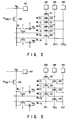
- Figs. 1 to 3 show circuits for realizing the quick AC burn-in test mode disclosed in Japanese Patent Application No. 2-418374.
- the circuit shown in Fig. 1 is used in a DRAM of a bootstrap word line driving scheme, in which a control clock signal ⁇ BOOT is caused to rise in the burn-in test mode to transfer charges, prestored in a bootstrap capacitor C BOOT , to selected word lines WLOi to WLi through n-channel MOS transistors 140 to 142.
- bits A0 to An of an address signal are set at "L" level in both "true and complementary” signals so as to simultaneously select a plurality of NOR type decoders 144 or 145, thereby simultaneously applying a voltage stress to word lines which are not adjacent to each other.
- the potential of a bit line BL is fixed at the ground potential through a transfer gate 146 and a pad 147 controlled by a bit line precharging signal ⁇ PRE .
- special voltage stress test pads 148 to 150 are arranged, and a transfer gate 151 or 152 is connected to one end of each of all word lines WL0i, WL1i,....
- the transfer gates 151 and 152 are selectively driven to select the even-numbered or odd-numbered word line group of the word line array, thereby simultaneously applying a voltage stress to the selected word line group (every other word line in the word line array) through the pad connected to the other end of each of the selected word lines.
- a voltage stress test cannot be performed with respect to a DRAM sealed in a package. In the circuits shown in Figs.
- a burn-in test In order to set the quick DC burn-in test mode in a wafer state or a packaged state of a DRAM without requiring special voltage stress test pads, as disclosed in Japanese Patent Application No. 2-418371, a burn-in test must be performed while signals on the input or output side of a word line selecting circuit are forcibly controlled to a constant level by externally inputting a control signal, and a larger number of word lines are simultaneously selected than in a normal operation.
- the number of circuits other than those required for the normal operation mode is preferably minimized to reduce an increase in chip area.
- not only a row decoder but also other circuits must or preferably be controlled simultaneously. Demands have arisen for practical measures to meet these requirements.
- the present invention has been made in consideration of the above situation, and has as its object to provide a semiconductor memory device in which the AC voltage stress test mode, in which the duty ratio at which a high voltage is applied to word lines in a wafer state or a packaged state is high, can be set, without using special voltage stress test pads, to minimize the number of circuits other than those required for a normal operation so as to reduce an increase in chip area, and failure modes which can occur in a normal operation but are difficult to predict, such as a decrease in breakdown voltage between adjacent word lines or adjacent bit lines, can be simultaneously screened by operating the device in substantially the same manner as in a normal operation.
- a semiconductor memory device comprises a DRAM circuit, a voltage stress test mode signal generating circuit for generating a voltage stress test mode signal on the basis of a predetermined signal input through some of external terminals used in a normal operation of the DRAM circuit, and a control circuit for receiving the test mode signal from the voltage stress test mode signal generating circuit, and performing control such that a plurality of bits of an output signal from a refresh address counter of the DRAM circuit are fixed at the same level, and bits other than the plurality of bits are subjected to a normal count operation.
- a semiconductor memory device comprises a DRAM circuit, a voltage stress test mode signal generating circuit for generating a voltage stress test mode signal on the basis of a predetermined signal input through some of external terminals used in a normal operation of the DRAM circuit, and a control circuit for receiving the test mode signal from the voltage stress test mode signal generating circuit, and performing control such that upper bits, of an output signal from a refresh address counter of the DRAM circuit, which are more significant than a specific bit are fixed at the same level, and lower bits which are less significant than the specific bit are subjected to a normal count operation.
- a semiconductor memory device comprises a DRAM circuit, a voltage stress test mode signal generating circuit for generating a voltage stress test mode signal on the basis of a predetermined signal input through some of external terminals used in a normal operation of the DRAM circuit, and a control circuit for receiving the test mode signal from the voltage stress test mode signal generating circuit, and performing control such that all bits of an output signal from a refresh address counter of the DRAM circuit are fixed at the same level so as to cause a word line driving circuit of the DRAM circuit to simultaneously drive all word lines.
- a voltage stress test mode signal is generated on the basis of a predetermined signal input through some of external terminals used in a normal operation of the DRAM circuit. Upon reception of this signal, only the upper bits of an output signal from the refresh address counter are fixed at the same level. In this case, since the lower bits of the output signal from the refresh address counter change in accordance with a counter operation, the AC voltage stress test mode can be set, in which the duty ratio at which a high voltage is applied to the word lines of the DRAM circuit is higher than that in a normal operation. Therefore, a decrease in breakdown voltage at the insulating film of the transfer gate of each memory cell can be screened in a short period of time.
- a voltage stress test mode signal is generated on the basis of a predetermined signal input through some of external terminals used in a normal operation of the DRAM circuit. Upon reception of this signal, all the bits of each of complementary output signals from the refresh address counter are fixed at the same level. With this operation, a desired voltage test mode (e.g., the quick DC burn-in test mode) can be set. As described above, no special pads are required to set a voltage stress test mode, and a voltage stress test mode can be set in a wafer state or a packaged state of a DRAM. In addition, the number of circuits other than those required for a normal operation can be minimized to reduce an increase in chip area.
- substantially the same operation means that the screening time is shortened by simultaneously selecting word lines in memory cell blocks which are considered to be independent with respect to a breakdown voltage reduction failure mode because the word lines of the respective blocks are sufficiently spaced apart from each other.
- Fig. 4 shows part of a DRAM incorporating a quick AC/DC burn-in test mode according to the first embodiment of the present invention.
- a DRAM circuit 10 has a quick AC/DC burn-in test mode in which AC/DC voltage stresses are simultaneously applied to word lines larger in number than those selected in a normal operation.
- the DRAM circuit 10 comprises: a memory cell array 1 having a plurality of dynamic memory cells arranged in the form of a matrix; word lines WL, each connected to memory cells in the same row; bit lines BL, each connected to memory cells in the same column; external terminals 2 (power supply terminal 2a to which a supply voltage is externally input, and input terminals 2b for receiving an address signal and various control signals (e.g., a write enable signal WE ⁇ , a row address strobe signal RAS ⁇ , and a column address strobe signal CAS ⁇ )); an address buffer circuit 3 for amplifying an external address signal input through some of the external terminals 2; a refresh address counter 4 for generating a refresh address signal for refreshing the memory cells; an address switching circuit 5 for selecting either an output signal from the refresh address counter 4 or a row address signal output from the address buffer circuit 3; a row decoder circuit (word line selecting circuit) 6 having a word line selecting function for selecting an arbitrary row in accordance with an internal row address signal
- the DRAM circuit 10 includes a fail-safe redundant arrangement (spare memory cells, spare word lines SWL, a spare row decoder, a word line driving circuit 13, and the like).
- the word line driving voltage source 7 is a booster circuit for generating a word line driving voltage VPP by boosting a supply voltage VCC, applied from the outside of the semiconductor chip, on the chip, and applying the word line driving voltage VPP as power to the word line driving circuit 8.
- a charge pump type booster circuit may be used as the word line driving voltage source 7
- a booster circuit having a large current driving capacity (constituted by, e.g., a ring oscillation circuit and a rectifying circuit) is preferably used.
- the DRAM circuit 10 may have a switching circuit (not shown) for selecting an output from the above-mentioned booster circuit in a normal operation, and selecting an externally applied word line driving voltage and applying the selected voltage as a word line driving voltage in a voltage stress test.
- this embodiment includes a VPP-VCC short circuit 14 for connecting the output node of the word line driving voltage source 7 to the power supply terminal 2a by short-circuiting so as to externally apply a word line driving voltage in a voltage stress test.
- a burn-in test mode signal generating circuit 20 generates a burn-in test mode signal BITAC/BITDC on the basis of a predetermined signal input through some of the external terminals 2 used in a normal operation of the DRAM circuit 10.
- the burn-in test mode signal BITAC/BITDC is set at high ("H") level in an active state, and is set at low ("L”) level in an inactive state.
- the burn-in test mode signal generating circuit 20 loads a row address signal input at the time when the RAS ⁇ signal is activated.
- the burn-in test mode signal generating circuit 20 sets the signal BITAC/BITDC at "H" level.
- a WCBR cycle is performed upon setting a normal supply voltage (e.g., 3V) for a normal operation
- the conventional multiple-bit parallel test mode is set.
- a WCBR cycle is performed upon setting a high supply voltage (e.g., 6V) falling outside a normal operation range
- the signal BITAC/BITDC is set at "H" level.
- the following mode setting scheme may be employed.
- the RAS ⁇ signal input is activated in a WCBR cycle upon setting a high supply voltage falling outside a normal operation range, some bits of the address signal constitute a predetermined combination (in the embodiment, both bits A0R and A1R are set "L" level), thereby setting the quick AC/DC burn-in test mode.
- the DRAM circuit 10 incorporates only the quick AC/DC burn-in test mode, the above-described complicated mode setting scheme need not be employed.
- the quick AC/DC burn-in test mode may be set when only a WCBR cycle is performed.
- a specific external terminal is set at a voltage other than a normal applied voltage (e.g., a voltage higher than a normal supply voltage: a super voltage), and the AC/DC burn-in test mode is set by detecting this voltage.
- a burn-in test mode control circuit 21 receives a burn-in test mode signal BITAC from the burn-in test mode signal generating circuit 20, and fixes only the upper bits of each of complementary output signals from the refresh address counter 4 of the DRAM circuit 10 at the same level, thereby setting an AC stress test mode (e.g., a quick AC burn-in test mode) in which the duty ratio at which a high voltage is applied to the word lines WL of the DRAM circuit 10 is higher than that in a normal operation.
- an AC stress test mode e.g., a quick AC burn-in test mode
- the burn-in test mode control circuit 21 receives a burn-in test mode signal BITDC from the burn-in test mode signal generating circuit 20, and fixes all the bits of an output signal from the refresh address counter 4 of the DRAM circuit 10 at the same level, thereby controlling the word line driving circuit 8 of the DRAM circuit 10 to simultaneously drive all the word lines (setting a quick DC burn-in test mode).
- the burn-in test mode control circuit 21 is preferably designed to control other circuits in proper circuit states in accordance with the AC burn-in test mode, in addition to receiving the burn-in test mode signal BITAC from the burn-in test mode signal generating circuit 20 to fix only the upper bits of each of complementary output signals from the refresh address counter 4 of the DRAM circuit 10 at the same level.
- the burn-in test mode control circuit 21 preferably performs control to selectively drive the spare word lines SWL at the same duty ratio as that for the normal word lines WL, and limits the capacity of a driving transistor for the sense amplifier SA to forcibly control the control signal ⁇ T at an active level (i.e., controlling the bit line transfer gate TG in an ON state in a voltage stress test).
- the burn-in test mode control circuit 21 is preferably designed to control other circuits in proper circuit states in accordance with the DC burn-in test mode, in addition to receiving the burn-in test mode BITDC from the burn-in test mode signal generating circuit 20 to fix all the bits of each of complementary output signals from the refresh address counter 4 of the DRAM circuit 10 at the same level.
- the burn-in test mode control circuit 21 preferably performs control to selectively drive the spare word lines SWL, controls the control signal ⁇ T and the bit line equalizing signal EQL at an active level (i.e., controlling the bit line transfer gate TG and the bit line precharging/equalizing circuit 11 in an ON state in a voltage stress test), controls the bit precharging voltage VBL at a low level, and performs control to inhibit the operation of the sense amplifier SA and circuits on its output side (e.g., a buffer circuit connected to the data lines).
- the burn-in test mode signal BITAC is generated by the burn-in test mode signal generating circuit 20 on the basis of a predetermined signal input through some of the external terminals 2, of the DRAM circuit 10, used in a normal operation, only the upper bits of each output signal from the refresh address counter 4 of the DRAM circuit 10 are fixed at the same level, thereby setting the quick AC burn-in test mode.
- the AC voltage stress test mode can be set, in which the duty ratio at which a high voltage is applied to the word lines WL of the DRAM circuit 10 is higher than that in a normal operation, thereby allowing a quick screening test of a decrease in the breakdown voltage of the insulating film of the bit line transfer gate TG of each memory cell.
- burn-in test mode signal BITDC is generated on the basis of a predetermined signal input through some of the external terminals 2, of the DRAM circuit 10, used in a normal operation, all the bits of each of complementary output signals from the refresh address counter 4 of the DRAM circuit 10 are fixed at the same level, thereby setting the quick DC burn-in test mode.
- the quick burn-in test mode can be set in a wafer state or after packaging. For this reason, in a quick AC/DC burn-in test in a wafer state, test units (e.g., a probe card) used for a normal function test can be used. In a quick AC/DC burn-in test after packaging, a general memory tester can be used.
- test units e.g., a probe card
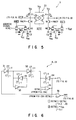
- Fig. 5 is a circuit diagram showing part of a row address buffer (corresponding to one bit) of the address buffer circuit 3 in Fig. 4.
- VCC denotes a supply potential
- VSS a ground potential
- P1 a p-channel MOS transistor
- N1 to N5 n-channel MOS transistors
- C1 and C2 MOS capacitors through which the drains and sources of the n-channel MOS transistors are commonly connected to the VSS node.
- Reference numeral 22 denotes a differential latch circuit.
- Reference symbol RLTC ⁇ a latch control signal
- Vref a reference potential
- RACP and RHLD ⁇ gate control signals
- AIjR and AIjR ⁇ complementary row address buffer output signals.
- Figs. 6 and 7 are circuit diagrams respectively showing part (corresponding to one stage) of the refresh address counter 4 and the burn-in test mode control circuit 21 in Fig. 4.
- reference numerals 31 to 34 denote clocked inverters; and 35, an inverter.
- two-input NOR gates 36 as part of the burn-in test mode control circuit 21 are inserted between the complementary output terminals of the respective stages of the address counter.
- This signal BITACj is set as follows. Assume that in the DRAM circuit 10 in Fig.
- the shared sense amplifier scheme in which the sense amplifier SA is used according to the time division scheme between adjacent memory cell blocks, is not employed, or the transfer gate control signal ⁇ T is forcibly set at "H" level in the AC burn-in test mode, as will be described later.
- the shared sense amplifier scheme is employed to use the 8th bit of the address counter output so as to perform address selection of cell blocks on both sides of the sense amplifier SA, and that the transfer gate control signal ⁇ T is not forcibly set at "H" level in the AC burn-in test mode, as will be described later.
- the signal BITDC is input to one input terminal of each of the NOR gates 36.
- Reference symbols CTj and CTj ⁇ denote complementary output signals from the address counter 4.
- Fig. 8 is a circuit diagram showing part (corresponding to one bit) of the address switching circuit 5 in Fig. 4.
- reference numeral 41 denotes an address switching NMOS transistor; and 42, an inverter for a latch circuit.
- Reference symbol RTRS ⁇ denotes a switching signal for selecting a row address buffer output; CT, a switching signal for selecting an address counter output; and AjR and AjR ⁇ , selection outputs (internal row address signals).
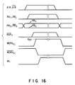
- the circuits shown in Figs. 5 to 8 are logically designed to realize operations such as those indicated by the timing charts shown in Figs. 9, 10, 11, and 12 in accordance with the normal operation mode, refresh operation mode, quick AC burn-in test mode, and quick DC burn-in test mode of the DRAM.
- the state of the row address buffer circuit 3 is determined by signals RACP, RHLD ⁇ , RLTC ⁇ , RTRS ⁇ , AIjR, and AIjR ⁇ .
- the signal BITAC/BITDC is at "L" level
- the DRAM circuit 10 operates in the same manner as the conventional DRAM. More specifically, in loading a column address signal by activating the signal CAS ⁇ signal after loading a row address signal by activating the signal RAS ⁇ , the signal CT is kept at "L” level, and the signal RTRS ⁇ is kept at "H” level. With this operation, the row address buffer output signals AIjR and AIjR ⁇ are selected and loaded as the internal row address signals AjR and AjR ⁇ .
- Fig. 10 shows an automatic refresh operation based on the execution of a CBR cycle (i.e., activating the signal CAS ⁇ earlier than the signal RAS ⁇ ).
- the signal RTRS ⁇ is immediately set at "L" level to inhibit selection of the row address buffer output signals AIjR and AIjR ⁇ .
- the signal CT is activated to select the output signals CTj and CTj ⁇ stored in the address counter 4 at this time so as to load them as internal row address signals RABj and RABj ⁇ , thus refreshing memory cells selected by the resulting word line selection signal.
- Figs. 13A and 14A are circuit diagrams exemplifying the burn-in test mode signal generating circuit 20.
- reference symbol WCBR denotes a signal generated when a clock for a WCBR cycle is input
- A0R ⁇ and A1R ⁇ bits of an internal row address signal obtained when the signal input RAS ⁇ is activated
- ROR a signal generated when a clock for an ROR cycle (an RAS only refresh cycle for temporarily activating only the signal RAS ⁇ ) is input.
- Reference numeral 61 denotes a three-input NAND gate; 62, a flip-flop circuit; and 63, an inverter.
- the bit A1R of an internal row address signal is input, instead of the bit A1R ⁇ in Fig. 13A, to generate the signal BITDC.
- the circuit shown in Fig. 13A is logically designed to realize an operation such as the one indicated by the timing chart shown in Fig. 13B. More specifically, if a WCBR cycle is performed when both the bits A0R and A1R of an address signal are set at "L" level, the signal BITAC is set at "H” level. When an ROR cycle is executed upon completion of the AC burn-in test mode, the signal BITAC goes to "L" level.
- the circuit shown in Fig. 14A is logically designed to realize an operation such as the one indicated by the timing chart shown in Fig. 14B.
- Fig. 15 is a circuit diagram showing part of the row decoder circuit 6 and the word line driving circuit 8 in Fig. 4.
- reference symbols PRn and PRn ⁇ denote precharging signals for a cell block n .
- Reference numeral 70 denotes a differential circuit.
- Reference symbol PRCHP denotes a precharging signal output from the differential circuit 70.
- a NAND circuit 73 has a precharging PMOS transistor load having a gate to which the signal PRCHP is input, and decodes the signal XAi, the signal XBj, and a signal RSPn ⁇ (for permitting selection of the word lines WL).
- a NAND circuit 74 has a precharging PMOS transistor load having a gate to which the signal PRCHP is input, and decodes a signal obtained by combining the bits A0R, A0R ⁇ , A1R, and A1R ⁇ of internal address signals, and the signal RSPn ⁇ .
- Four NAND circuits 74 are arranged for one cell block in the embodiment.
- a first word line driving circuit 75 is selectively driven by an output from the NAND circuit (row decoder) 74.
- a second word line driving circuit 76 is selectively driven by an output from the NAND circuit (row decoder) 73.
- Reference symbol WLOn denotes a word line (there are four word lines per cell block in the embodiment) having one end connected to a corresponding one of the output nodes of the first word line driving circuit 75, and the other end connected to a driving voltage source node of the second word line driving circuit 76; WDRVn, the voltage of the word line WLOn; WDRVnj ⁇ , a voltage obtained by inverting the level of the word line voltage WDRVnj; and WL, a word line having one end connected to a corresponding one of the output nodes of the second word line driving circuit 76.
- the first word line driving circuit 75 comprises a word line driving PMOS transistor TP connected between a driving voltage source node and the word line WLOn, an NMOS transistor 77 connected between the word line and a VSS node, a pull-up PMOS transistor 78 connected between a VCC node and a driving circuit input node, and an inverter 79 connected between the driving circuit input node and the gate of the pull-up PMOS transistor 78.
- the second word line driving circuit 76 comprises a word line driving PMOS transistor TP connected to a driving voltage source node and the word line WL, an NMOS transistor 77 connected between the word line and a VSS node, a pull-up PMOS transistor 78 connected to a VCC node and a driving circuit input node, an inverter 79 connected between the driving circuit input node and the gate of the pull-up PMOS transistor 78, and a noise killer NMOS transistor TN connected to one end of the word line WL and having a gate to which the word line voltage WDRVnj ⁇ is input.
- the gate potentials of all the word line driving PMOS transistors TP whose sources have received the word line voltage WDRVnj are set at "L" level.
- one of the word lines WLOi is selected and set at "H” level in accordance with the states of the address bits A0R and A1R selected by an output signal from the refresh address counter 4 in a CBR cycle
- one of the word lines WL is selected by the second word line driving circuit 76. If all the n memory cell blocks are set in a selected state at this time, every fifth word line WL rises in the word line arrays of all the blocks. By repeating the CBR cycle, another set of word lines rise. If the CBR cycle is repeated four times, all the word lines WL rise.
- every ninth word line WL rises in the word line arrays of all the blocks. If the logical arrangement is modified to change only the least significant bit of each address counter output, every second word line WL rises in the word line arrays of all the blocks.
- Fig. 17 is a circuit diagram exemplifying the spare row decoder/word line driving circuit 13 in Fig. 4.
- reference numeral 81 denotes a NOR input NMOS transistor. An address signal to be decoded is input to the gate of each NMOS transistor 81. The source of each transistor 81 is grounded. The drains of the respective transistors 81 are connected together through fuse elements F consisting of, e.g., polysilicon. The fuses F are disconnected in accordance with an address to be decoded.
- Reference numeral 82 denotes a precharging PMOS transistor 82; 83, a pull-up PMOS transistor; 84, an inverter; and 85, a NAND gate.
- the circuit shown in Fig. 17 is logically designed to realize the following operation.
- a signal RSP ⁇ is set at "L” level
- a signal RSP is set at "H” level.
- a sync signal XVLD goes from “L” level to "H” level in a block selected by a block selection signal RSLn
- the signal RSP ⁇ is kept at “L” level
- a signal SWSn goes from “L” level to "H” level.
- Figs. 18 and 19 are circuit diagrams showing a one-column portion of the memory cell array 1 in Fig. 4 and part of a memory cell peripheral circuit.
- Figs. 18 and 19 show two memory cells MC as representatives of the memory cells arranged in the form of a matrix.
- Each memory cell MC includes a capacitor C having one end connected to the source of a transfer gate MOS transistor (cell transistor), and the other end connected to a capacitor line (e.g., a plate potential VPL).
- Word lines WLni and WL(n+1)j are connected to the gates of the cell transistors T in the same row.
- Bit lines BLnk and BLnk ⁇ are connected to the drains of the cell transistors T in the same column.
- the sense amplifier SA for example, a latch type circuit constituted by an n-channel sense amplifier NSA and a p-channel sense amplifier PSA is used.
- Reference numerals 91 denote two activation control (driving) transistors for the n-channel sense amplifier NSA; 92, two activation control (driving) transistors for the p-channel sense amplifier PSA; 93, inverters; 94, AND gates; and 95, NAND gates.
- Each bit line transfer gate TG is constituted by an NMOS transistor inserted between a pair of input nodes of a corresponding one of the sense amplifiers SA and a pair of bit lines BL and BL ⁇ .
- the transfer gate control signal ⁇ T By inputting the transfer gate control signal ⁇ T to the gate of this transistor, connection between the sense amplifiers SA and a pair of bit lines BL and BL ⁇ is controlled.
- a column selection circuit transfer gate controlled by a column selection line (not shown) to transfer information, amplified by the sense amplifier SA, to a data line pair (not shown) is omitted.
- the bit line precharging/equalizing circuit 11 is controlled by the bit line equalizing signal EQL to precharge a pair of bit lines BL and BL ⁇ on both sides of the sense amplifier SA to the bit precharging voltage VBL, thus equalizing their potentials.
- a CENB ⁇ signal generating circuit 96 generates a signal CENB ⁇ for activating the operations of the sense amplifier SA and a circuit on the output side (e.g., in a read operation, a column address is loaded to cause a column selection line to rise, and a buffer circuit (not shown) connected to a data line pair is activated to amplify information of the data line pair and transfer the information to an output buffer circuit (not shown), thus outputting the information outside the chip).
- the circuit shown in Fig. 18 is logically designed to realize the following operation.
- the n-channel sense amplifier NSA is activated while the driving transistors 91 for the n-channel sense amplifier NSA are optimized (in the embodiment, the amplifier is activated by the sum of the driving forces of the two driving transistors 91).
- the p-channel sense amplifier PSA is activated while the driving transistors 92 for the p-channel sense amplifier PSA are optimized (in the embodiment, the amplifier is activated by the sum of the driving forces of the two driving transistors 92).
- the circuit shown in Fig. 19 is logically designed to realize the following operation.
- the signal BITDC is at "L" level
- the n-channel sense amplifier NSA is activated.
- the sense amplifier activating signal SEP rises, the p-channel sense amplifier PSA is activated.
- the signal CENB ⁇ goes to "L” level to start the operation of the column system.
- the signal BITDC is set at "H” level, neither of the n- and p-channel amplifiers NSA and PSA are activated, and the signal CENB ⁇ is kept at "H” level to inhibit the operation of the column system.
- Fig. 20 is a circuit diagram showing a signal generating circuit for generating the signals ⁇ T and EQL in Fig. 18.
- reference numerals 100 and 101 denote differential circuits; 102 to 108, inverters; and 109 to 111, NAND gates.
- a signal WLDOWN is kept at "H" level until the word line WL rises.
- the circuit shown in Fig. 20 is logically designed to realize the following operation.
- a signal BLHZ signal is set at “L” level in synchronism with a signal RSTR ⁇ which is set at "L” level immediately after the signal RAS ⁇ (the signal WLDOWN is irrelevant in this case because it is kept at "H” level until the word line WL rises) in a block selected by the block selection signal RSLn.
- the equalizing operation of a pair of bit lines BL ⁇ of the selected memory cell block is stopped to wait for the word line WL to rise.
- the signal BITAC When the signal BITAC is set at "H” level, the signal ⁇ T is forcibly clamped to "H” level for the following reason.
- the signal ⁇ T In the shared sense amplifier scheme, if adjacent memory cell blocks are simultaneously activated, the signal ⁇ T is turned off in both the blocks. As a result, data cannot be amplified by the sense amplifier SA.
- the row address counter for selecting adjacent memory cell blocks is arranged immediately above the address counter for the address bits A0 and A1 to perform address replacement, thereby allowing all the word lines WL to rise once for every eight CBR cycles.
- the circuit shown in Fig. 21 is logically designed to realize the following operation.
- a signal BLHZ signal is set at “L” level in synchronism with a signal RSTR ⁇ which is set at "L” level immediately after the signal RAS ⁇ (the signal WLDOWN is irrelevant in this case because it is kept at "H” level until the word line WL rises) in a block selected by the block selection signal RSLn.
- the equalizing operation of a pair of bit lines BL ⁇ of the selected memory cell block is stopped to wait for the word line WL to rise.
- the signal BITDC is set at "H” level
- both the signals ⁇ T and EQL are clamped to "H” level. With this operation, all the pairs of bit lines BL and BL ⁇ are set at the bit precharging voltage VBL.
- Fig. 22 is a circuit diagram exemplifying the VBL generating circuit 12 in Fig. 4.
- reference symbols P2 to P5 denote PMOS transistors; N6 to N10, NMOS transistors; and 111, an inverter circuit.
- the circuit in Fig. 22 is designed to realize the following operation.
- a potential VBL of 0.5 Vcc is output.
- the potential VBL is forcibly set at "L” level, thus fixing all the pairs of bit lines BL and BL ⁇ to "L" level.
- Fig. 23 is a circuit diagram exemplifying the word line driving voltage source 7 (VPP generating circuit) and the VPP-VCC short circuit 14 in Fig. 4.
- reference numeral 120 denotes a booster circuit for generating a potential VPP; 121, an inverter circuit; and 122, a NOR gate.
- Reference symbol CP denotes a capacitive element; D, a diode; R1 and R2, resistive elements; 123, a PMOS transistor; 124, a differential circuit; and 125, a comparator.
- the circuit shown in Fig. 23 is designed to realize the following operation.
- the PMOS transistor 123 between a VPP line and a VCC line in an OFF state and the booster circuit 120 between he VPP line and the VCC line operates to boost the word line driving voltage VPP to a limit potential corresponding to a reference potential Vref1 in the chip.
- the signal BITAC/BITDC is set at "H” level
- the booster circuit 120 is inactivated, and the VPP-VCC short circuit 14 is activated instead.
- the word line driving potential VPP becomes equal to the external supply potential VCC.
- a DRAM according to the second embodiment of the present invention will be described next, which uses a voltage decreasing circuit for applying a supply voltage VCC, applied from the outside of the chip, as a word line driving voltage, and applying an internal decreased voltage VDD, obtained by decreasing the supply voltage VCC on the chip, as power to a memory cell peripheral circuit.
- a VCC-VDD short circuit 131 is preferably arranged to connect the output node of a voltage decreasing circuit 130 and an external power terminal by, e.g., short-circuiting in the AC/DC burn-in test mode.
- Fig. 24 is a circuit diagram exemplifying the voltage decreasing circuit 130 and the VCC-VDD short circuit 131.
- reference numeral 132 denotes an inverter; 133 and 134, PMOS transistors; and 135, comparators.
- Reference symbols R3 and R4 denote resistive elements.
- Fig. 25 is a timing chart showing a cycle for setting a quick AC burn-in test mode, an AC stress test cycle, and a cycle for terminating a test in the above-described DRAM of the present invention.
- the quick AC burn-in test mode is executed according to the following steps.
- the same data is written in memory cells connected to a sense amplifier SA through a bit line BL in a normal write mode.
- a WCBR cycle is executed while address signal bits A0R and A1R are set at "L" level, thereby generating an AC burn-in test mode signal.
- a time interval tRP (several ⁇ s) long enough to complete the setting of the voltages VPP and VDD in the third step is ensured.
- the voltage VCC is boosted to a high voltage for performing a burn-in test.
- an AC stress is applied to the word lines WL for a required period of time the number of times corresponding to a plurality of sets, each set consisting of four or eight CBR cycles.
- a clock for an ROR cycle is input to terminate the AC burn-in test mode.
- Fig. 26 is a timing chart showing a cycle for setting a quick DC burn-in test mode, a DC stress test cycle, and a cycle for terminating a test in the above-described DRAM of the present invention.
- the quick DC burn-in test mode is executed according to the following steps.
- a WCBR cycle is executed, while the address signal bits A0R and A1R are set at "L" level and “H” level, respectively, thus generating a test mode signal.
- the signals CTj and CTj ⁇ are set at "L” level.
- a signal EQL and the signal ⁇ T are set at “H” level.
- Signals SEP and SEN are set at “L” level.
- the potential VBL is set at “L” level.
- a time interval tRP (several ⁇ s) long enough to complete the setting of the voltages VBL, VPP, and VDD in the second step is ensured.
- the voltage VCC is boosted to a high voltage for performing a burn-in test.
- a long CBR cycle is executed to simultaneously apply a DC stress to all the word lines WL for a required period of time.
- a clock for an ROR is input to terminate the DC burn-in test mode.
- the voltage stress test in the burn-in test mode is exemplified. It is, however, apparent that the present invention is effective in performing a voltage stress test regardless of temperature acceleration.
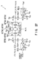
- Fig. 27 is a circuit diagram showing a modification of part of the row address buffer (corresponding to one bit) of the address buffer circuit 3 shown in Fig. 4.
- the components identical to those shown in Fig. 5 are denoted by the same numerals.
- the BITDC and BITDC ⁇ signals are input to all row address buffers in the DC burn-in test mode.
- the lower order row addresses AI0R and AI1R required for selecting every forth word line WL are inputted into the row address buffer shown in Fig. 5 instead of the row address buffer shown in Fig. 27.
- the row address buffer of Fig. 5 is used to output the output signals AI0R, AI0R ⁇ , and the output signals AI1R, AI1R ⁇
- the row address buffer of Fig. 27 is employed to output the output signals AI2R and AI2R ⁇ and output signals of higher orders.
- the semiconductor storage device of the present invention in setting the AC voltage stress test mode in which the duty ratio at which a high voltage is applied to word lines in a wafer state or after packaging is high, no special voltage stress test pads are required, and the number of circuits other than those required for the normal operation mode can be minimized, thereby suppressing an increase in chip area.
- failure modes which can occur in a normal operation but are difficult to predict such as a decrease in break-down voltage between adjacent word lines or adjacent bit lines, can be simultaneously screened by operating the device in substantially the same manner as in a normal operation, thereby allowing quick screening of the overall chip under conditions similar to those in a normal operation.
- the semiconductor storage device of the present invention in setting a desired DC voltage stress test mode in which the duty ratio at which a high voltage is applied to word lines in a wafer state or after packaging is high, no special voltage stress test pads are required, and the number of circuits other than those required for the normal operation mode can be minimized, thereby reducing an increase in chip area.
Landscapes
- For Increasing The Reliability Of Semiconductor Memories (AREA)
- Dram (AREA)
Applications Claiming Priority (4)
| Application Number | Priority Date | Filing Date | Title |
|---|---|---|---|
| JP04153482A JP3135681B2 (ja) | 1992-06-12 | 1992-06-12 | 半導体記憶装置 |
| JP153485/92 | 1992-06-12 | ||
| JP153482/92 | 1992-06-12 | ||
| JP04153485A JP3105078B2 (ja) | 1992-06-12 | 1992-06-12 | 半導体記憶装置 |
Publications (3)
| Publication Number | Publication Date |
|---|---|
| EP0574002A2 true EP0574002A2 (de) | 1993-12-15 |
| EP0574002A3 EP0574002A3 (de) | 1995-03-15 |
| EP0574002B1 EP0574002B1 (de) | 1998-08-19 |
Family
ID=26482088
Family Applications (1)
| Application Number | Title | Priority Date | Filing Date |
|---|---|---|---|
| EP93109368A Expired - Lifetime EP0574002B1 (de) | 1992-06-12 | 1993-06-11 | Halbleiter-Speichergerät mit Spannungstressprüfmodus |
Country Status (4)
| Country | Link |
|---|---|
| US (1) | US5381373A (de) |
| EP (1) | EP0574002B1 (de) |
| KR (1) | KR950014099B1 (de) |
| DE (1) | DE69320416T2 (de) |
Cited By (12)
| Publication number | Priority date | Publication date | Assignee | Title |
|---|---|---|---|---|
| EP0669619A3 (de) * | 1994-02-25 | 1995-10-04 | Toshiba Kk | |
| EP0745998A1 (de) * | 1995-05-31 | 1996-12-04 | United Memories, Inc. | Schaltung und Verfahren zum Zugriff auf Speicherzellen einer Speicheranordnung |
| EP0766259A3 (de) * | 1995-09-28 | 1997-11-05 | International Business Machines Corporation | Dynamischer Direktzugriffspeicher |
| GB2316751A (en) * | 1996-08-29 | 1998-03-04 | Samsung Electronics Co Ltd | Internal source voltage generating circuit for a semiconductor memory device |
| GB2317456A (en) * | 1996-09-23 | 1998-03-25 | Samsung Electronics Co Ltd | Wafer burn-in test circuit for a semiconductor memory device |
| GB2287326B (en) * | 1994-03-10 | 1998-04-22 | Samsung Electronics Co Ltd | Semiconductor integrated circuit |
| GB2319623A (en) * | 1996-11-06 | 1998-05-27 | Hyundai Electronics Ind | A wafer burn-in test circuit for a semiconductor memory |
| DE19735406A1 (de) * | 1997-08-14 | 1999-02-18 | Siemens Ag | Halbleiterbauelement und Verfahren zum Testen und Betreiben eines Halbleiterbauelementes |
| US6445630B2 (en) | 2000-03-23 | 2002-09-03 | Infineon Technologies Ag | Method for carrying out a burn-in process for electrically stressing a semiconductor memory |
| KR100355225B1 (ko) * | 1999-07-12 | 2002-10-11 | 삼성전자 주식회사 | 교류 스트레스의 번-인 테스트가 가능한 집적회로 및 이를 이용한 테스트 방법 |
| EP0978846A3 (de) * | 1998-08-03 | 2005-06-08 | International Business Machines Corporation | Wortleitungsaktivierung von Zeitsignalen für Gleichstrom -Einbrennung eines DRAM mit Selbstauffrischung |
| CN110875079A (zh) * | 2018-09-03 | 2020-03-10 | 瑞萨电子株式会社 | 半导体器件 |
Families Citing this family (40)
| Publication number | Priority date | Publication date | Assignee | Title |
|---|---|---|---|---|
| KR0119887B1 (ko) * | 1994-06-08 | 1997-10-30 | 김광호 | 반도체 메모리장치의 웨이퍼 번-인 테스트 회로 |
| KR0135108B1 (ko) * | 1994-12-13 | 1998-04-25 | 김광호 | 스트레스 테스트 회로를 포함하는 반도체 메모리 장치 |
| US6041426A (en) * | 1995-04-07 | 2000-03-21 | National Semiconductor Corporation | Built in self test BIST for RAMS using a Johnson counter as a source of data |
| US5689466A (en) * | 1995-04-07 | 1997-11-18 | National Semiconductor Corporation | Built in self test (BIST) for multiple RAMs |
| US5568435A (en) * | 1995-04-12 | 1996-10-22 | Micron Technology, Inc. | Circuit for SRAM test mode isolated bitline modulation |
| US5657284A (en) * | 1995-09-19 | 1997-08-12 | Micron Technology, Inc. | Apparatus and method for testing for defects between memory cells in packaged semiconductor memory devices |
| US5965902A (en) * | 1995-09-19 | 1999-10-12 | Micron Technology | Method and apparatus for testing of dielectric defects in a packaged semiconductor memory device |
| JPH09147599A (ja) * | 1995-11-28 | 1997-06-06 | Mitsubishi Electric Corp | 半導体記憶装置 |
| US6059450A (en) * | 1996-12-21 | 2000-05-09 | Stmicroelectronics, Inc. | Edge transition detection circuitry for use with test mode operation of an integrated circuit memory device |
| US6079037A (en) | 1997-08-20 | 2000-06-20 | Micron Technology, Inc. | Method and apparatus for detecting intercell defects in a memory device |
| US6094734A (en) * | 1997-08-22 | 2000-07-25 | Micron Technology, Inc. | Test arrangement for memory devices using a dynamic row for creating test data |
| KR100269322B1 (ko) * | 1998-01-16 | 2000-10-16 | 윤종용 | 스트레스용전압을이용하여메모리를테스팅하는기능을갖는집적회로및그의메모리테스트방법 |
| KR100267781B1 (ko) * | 1998-03-04 | 2000-10-16 | 김영환 | 테스트 모드를 셋업하기 위한 반도체 소자 |
| US6122760A (en) * | 1998-08-25 | 2000-09-19 | International Business Machines Corporation | Burn in technique for chips containing different types of IC circuitry |
| US6055199A (en) * | 1998-10-21 | 2000-04-25 | Mitsubishi Denki Kabushiki Kaisha | Test circuit for a semiconductor memory device and method for burn-in test |
| KR100343283B1 (ko) * | 1999-07-02 | 2002-07-15 | 윤종용 | 반도체 장치의 테스트 전원 공급 회로 |
| JP2001067898A (ja) * | 1999-08-30 | 2001-03-16 | Mitsubishi Electric Corp | 半導体記憶装置 |
| TW432574B (en) * | 2000-01-19 | 2001-05-01 | Yang Wen Kun | Wafer level burn in device and method |
| US6535014B2 (en) | 2000-01-19 | 2003-03-18 | Lucent Technologies, Inc. | Electrical parameter tester having decoupling means |
| JP2002074991A (ja) * | 2000-08-31 | 2002-03-15 | Fujitsu Ltd | メモリを有する半導体装置 |
| JP2002124096A (ja) * | 2000-10-13 | 2002-04-26 | Nec Corp | 半導体記憶装置及びその試験方法 |
| JP2003030999A (ja) * | 2001-07-18 | 2003-01-31 | Mitsubishi Electric Corp | 半導体記憶装置 |
| US6763314B2 (en) | 2001-09-28 | 2004-07-13 | International Business Machines Corporation | AC defect detection and failure avoidance power up and diagnostic system |
| KR100413242B1 (ko) * | 2001-12-20 | 2004-01-03 | 주식회사 하이닉스반도체 | 웨이퍼 번인 테스트 모드 회로 |
| KR100442960B1 (ko) * | 2001-12-21 | 2004-08-04 | 주식회사 하이닉스반도체 | 반도체 메모리 테스트 장치 |
| US6728156B2 (en) * | 2002-03-11 | 2004-04-27 | International Business Machines Corporation | Memory array system |
| US6791348B2 (en) * | 2002-07-29 | 2004-09-14 | International Business Machines Corporation | Digital overcurrent test |
| KR100835279B1 (ko) * | 2006-09-05 | 2008-06-05 | 삼성전자주식회사 | 수직 채널 구조를 가지는 트랜지스터를 구비하는 반도체메모리 장치 |
| US7742351B2 (en) * | 2006-06-30 | 2010-06-22 | Semiconductor Energy Laboratory Co., Ltd. | Semiconductor device and electronic device |
| KR100904962B1 (ko) * | 2007-05-31 | 2009-06-26 | 삼성전자주식회사 | 스트레스 검출 회로, 이를 포함하는 반도체 칩 및 스트레스검출 방법 |
| JP5405007B2 (ja) * | 2007-07-20 | 2014-02-05 | ピーエスフォー ルクスコ エスエイアールエル | 半導体装置 |
| KR100845810B1 (ko) | 2007-08-14 | 2008-07-14 | 주식회사 하이닉스반도체 | 웨이퍼 번인 테스트 회로 |
| US7924633B2 (en) * | 2009-02-20 | 2011-04-12 | International Business Machines Corporation | Implementing boosted wordline voltage in memories |
| US8462571B2 (en) * | 2011-07-19 | 2013-06-11 | Elite Semiconductor Memory Technology Inc. | DRAM and method for testing the same in the wafer level burn-in test mode |
| US8907687B2 (en) * | 2012-05-03 | 2014-12-09 | Globalfoundries Inc. | Integrated circuit with stress generator for stressing test devices |
| US20140032826A1 (en) * | 2012-07-25 | 2014-01-30 | Samsung Electronics Co., Ltd. | Method of training memory core and memory system |
| US9183951B2 (en) * | 2013-09-11 | 2015-11-10 | Tsuneo Inaba | Resistance change memory and test method of the same |
| JP2015118724A (ja) * | 2013-11-13 | 2015-06-25 | 株式会社半導体エネルギー研究所 | 半導体装置及び半導体装置の駆動方法 |
| US11837313B2 (en) | 2021-11-02 | 2023-12-05 | Qualcomm Incorporated | Memory with efficient DVS controlled by asynchronous inputs |
| CN115472207A (zh) * | 2022-09-23 | 2022-12-13 | 武汉新芯集成电路制造有限公司 | 存储芯片及操作方法 |
Family Cites Families (4)
| Publication number | Priority date | Publication date | Assignee | Title |
|---|---|---|---|---|
| US4661930A (en) * | 1984-08-02 | 1987-04-28 | Texas Instruments Incorporated | High speed testing of integrated circuit |
| JPS61258399A (ja) * | 1985-05-11 | 1986-11-15 | Fujitsu Ltd | 半導体集積回路装置 |
| US5258954A (en) * | 1989-06-30 | 1993-11-02 | Kabushiki Kaisha Toshiba | Semiconductor memory including circuitry for driving plural word lines in a test mode |
| JP2945508B2 (ja) * | 1991-06-20 | 1999-09-06 | 三菱電機株式会社 | 半導体装置 |
-
1993
- 1993-06-10 KR KR1019930010501A patent/KR950014099B1/ko not_active Expired - Fee Related
- 1993-06-11 DE DE69320416T patent/DE69320416T2/de not_active Expired - Fee Related
- 1993-06-11 US US08/075,313 patent/US5381373A/en not_active Expired - Lifetime
- 1993-06-11 EP EP93109368A patent/EP0574002B1/de not_active Expired - Lifetime
Cited By (23)
| Publication number | Priority date | Publication date | Assignee | Title |
|---|---|---|---|---|
| US5592421A (en) * | 1994-02-25 | 1997-01-07 | Kabushiki Kaisha Toshiba | Semiconductor integrated circuit for generating an internal power source voltage with reduced potential changes |
| EP0669619A3 (de) * | 1994-02-25 | 1995-10-04 | Toshiba Kk | |
| GB2287326B (en) * | 1994-03-10 | 1998-04-22 | Samsung Electronics Co Ltd | Semiconductor integrated circuit |
| EP0745998A1 (de) * | 1995-05-31 | 1996-12-04 | United Memories, Inc. | Schaltung und Verfahren zum Zugriff auf Speicherzellen einer Speicheranordnung |
| US5680362A (en) * | 1995-05-31 | 1997-10-21 | United Memories, Inc. | Circuit and method for accessing memory cells of a memory device |
| EP0766259A3 (de) * | 1995-09-28 | 1997-11-05 | International Business Machines Corporation | Dynamischer Direktzugriffspeicher |
| GB2316751B (en) * | 1996-08-29 | 1999-04-07 | Samsung Electronics Co Ltd | Internal source voltage generating circuit |
| GB2316751A (en) * | 1996-08-29 | 1998-03-04 | Samsung Electronics Co Ltd | Internal source voltage generating circuit for a semiconductor memory device |
| US6266286B1 (en) | 1996-09-23 | 2001-07-24 | Samsung Electronics Co., Ltd. | Wafer burn-in test circuit and method for testing a semiconductor memory device |
| GB2317456B (en) * | 1996-09-23 | 1998-12-23 | Samsung Electronics Co Ltd | Wafer burn-in test circuit of semiconductor memory device |
| GB2317456A (en) * | 1996-09-23 | 1998-03-25 | Samsung Electronics Co Ltd | Wafer burn-in test circuit for a semiconductor memory device |
| US6026038A (en) * | 1996-09-23 | 2000-02-15 | Samsung Electronics Co., Ltd. | Wafer burn-in test circuit and method for testing a semiconductor memory |
| US5936899A (en) * | 1996-11-06 | 1999-08-10 | Hyundai Electronics Industries Co., Ltd. | Wafer burn-in test circuit of a semiconductor memory device |
| GB2319623A (en) * | 1996-11-06 | 1998-05-27 | Hyundai Electronics Ind | A wafer burn-in test circuit for a semiconductor memory |
| GB2319623B (en) * | 1996-11-06 | 2001-03-28 | Hyundai Electronics Ind | Wafer burn-in test circuit of a semiconductor memory device |
| DE19735406A1 (de) * | 1997-08-14 | 1999-02-18 | Siemens Ag | Halbleiterbauelement und Verfahren zum Testen und Betreiben eines Halbleiterbauelementes |
| US6313655B1 (en) | 1997-08-14 | 2001-11-06 | Infineon Technologies Ag | Semiconductor component and method for testing and operating a semiconductor component |
| EP0978846A3 (de) * | 1998-08-03 | 2005-06-08 | International Business Machines Corporation | Wortleitungsaktivierung von Zeitsignalen für Gleichstrom -Einbrennung eines DRAM mit Selbstauffrischung |
| KR100355225B1 (ko) * | 1999-07-12 | 2002-10-11 | 삼성전자 주식회사 | 교류 스트레스의 번-인 테스트가 가능한 집적회로 및 이를 이용한 테스트 방법 |
| US6490223B1 (en) | 1999-07-12 | 2002-12-03 | Samsung Electronics Co., Ltd. | Integrated circuit capable of being burn-in tested using an alternating current stress and a testing method using the same |
| US6816429B2 (en) | 1999-07-12 | 2004-11-09 | Samsung Electronics Co., Ltd. | Integrated circuit capable of being burn-in tested using an alternating current stress and a testing method using the same |
| US6445630B2 (en) | 2000-03-23 | 2002-09-03 | Infineon Technologies Ag | Method for carrying out a burn-in process for electrically stressing a semiconductor memory |
| CN110875079A (zh) * | 2018-09-03 | 2020-03-10 | 瑞萨电子株式会社 | 半导体器件 |
Also Published As
| Publication number | Publication date |
|---|---|
| DE69320416D1 (de) | 1998-09-24 |
| EP0574002A3 (de) | 1995-03-15 |
| US5381373A (en) | 1995-01-10 |
| KR940006150A (ko) | 1994-03-23 |
| KR950014099B1 (ko) | 1995-11-21 |
| DE69320416T2 (de) | 1999-02-04 |
| EP0574002B1 (de) | 1998-08-19 |
Similar Documents
| Publication | Publication Date | Title |
|---|---|---|
| EP0574002B1 (de) | Halbleiter-Speichergerät mit Spannungstressprüfmodus | |
| US6414890B2 (en) | Semiconductor memory device capable of reliably performing burn-in test at wafer level | |
| KR960000888B1 (ko) | 반도체 기억 장치 | |
| JP2885597B2 (ja) | 半導体メモリ | |
| US4449207A (en) | Byte-wide dynamic RAM with multiplexed internal buses | |
| JP2781149B2 (ja) | 半導体メモリのストレス回路及びストレス電圧供給方法 | |
| US5694364A (en) | Semiconductor integrated circuit device having a test mode for reliability evaluation | |
| EP0585870A2 (de) | Dynamischer RAM mit Spannungsstressanlegeschaltung | |
| JP3736714B2 (ja) | 半導体メモリのウエハバーンインテスト回路 | |
| US5808955A (en) | Integrated circuit memory devices including sub-word line drivers and related methods | |
| US6327198B1 (en) | Semiconductor memory device having a test mode setting circuit | |
| JP2829135B2 (ja) | 半導体記憶装置 | |
| US5936910A (en) | Semiconductor memory device having burn-in test function | |
| US5698876A (en) | Memory standard cell macro for semiconductor device | |
| US5428576A (en) | Semiconductor device and method of screening the same | |
| JP2829134B2 (ja) | 半導体記憶装置 | |
| KR100438237B1 (ko) | 테스트 회로를 갖는 반도체 집적 회로 | |
| JP3105078B2 (ja) | 半導体記憶装置 | |
| JP2004199778A (ja) | 半導体記憶装置 | |
| JPH09320296A (ja) | 半導体記憶装置 | |
| JP3135681B2 (ja) | 半導体記憶装置 | |
| US6430091B2 (en) | Semiconductor memory device having reduced current consumption at internal boosted potential | |
| JP2000030455A (ja) | 半導体記憶装置 | |
| JP2965881B2 (ja) | 半導体記憶装置 | |
| JPH11317097A (ja) | 半導体記憶装置 |
Legal Events
| Date | Code | Title | Description |
|---|---|---|---|
| PUAI | Public reference made under article 153(3) epc to a published international application that has entered the european phase |
Free format text: ORIGINAL CODE: 0009012 |
|
| 17P | Request for examination filed |
Effective date: 19930611 |
|
| AK | Designated contracting states |
Kind code of ref document: A2 Designated state(s): DE FR GB |
|
| PUAL | Search report despatched |
Free format text: ORIGINAL CODE: 0009013 |
|
| AK | Designated contracting states |
Kind code of ref document: A3 Designated state(s): DE FR GB |
|
| 17Q | First examination report despatched |
Effective date: 19970416 |
|
| GRAG | Despatch of communication of intention to grant |
Free format text: ORIGINAL CODE: EPIDOS AGRA |
|
| GRAG | Despatch of communication of intention to grant |
Free format text: ORIGINAL CODE: EPIDOS AGRA |
|
| GRAH | Despatch of communication of intention to grant a patent |
Free format text: ORIGINAL CODE: EPIDOS IGRA |
|
| GRAH | Despatch of communication of intention to grant a patent |
Free format text: ORIGINAL CODE: EPIDOS IGRA |
|
| GRAA | (expected) grant |
Free format text: ORIGINAL CODE: 0009210 |
|
| AK | Designated contracting states |
Kind code of ref document: B1 Designated state(s): DE FR GB |
|
| REF | Corresponds to: |
Ref document number: 69320416 Country of ref document: DE Date of ref document: 19980924 |
|
| ET | Fr: translation filed | ||
| PLBE | No opposition filed within time limit |
Free format text: ORIGINAL CODE: 0009261 |
|
| STAA | Information on the status of an ep patent application or granted ep patent |
Free format text: STATUS: NO OPPOSITION FILED WITHIN TIME LIMIT |
|
| 26N | No opposition filed | ||
| REG | Reference to a national code |
Ref country code: GB Ref legal event code: IF02 |
|
| PGFP | Annual fee paid to national office [announced via postgrant information from national office to epo] |
Ref country code: GB Payment date: 20090610 Year of fee payment: 17 Ref country code: DE Payment date: 20090604 Year of fee payment: 17 |
|
| GBPC | Gb: european patent ceased through non-payment of renewal fee |
Effective date: 20100611 |
|
| REG | Reference to a national code |
Ref country code: FR Ref legal event code: ST Effective date: 20110228 |
|
| PG25 | Lapsed in a contracting state [announced via postgrant information from national office to epo] |
Ref country code: DE Free format text: LAPSE BECAUSE OF NON-PAYMENT OF DUE FEES Effective date: 20110101 |
|
| PG25 | Lapsed in a contracting state [announced via postgrant information from national office to epo] |
Ref country code: FR Free format text: LAPSE BECAUSE OF NON-PAYMENT OF DUE FEES Effective date: 20100630 |
|
| PG25 | Lapsed in a contracting state [announced via postgrant information from national office to epo] |
Ref country code: GB Free format text: LAPSE BECAUSE OF NON-PAYMENT OF DUE FEES Effective date: 20100611 |
|
| PGFP | Annual fee paid to national office [announced via postgrant information from national office to epo] |
Ref country code: FR Payment date: 20090611 Year of fee payment: 17 |