EP0574812A2 - Procédé de conversion analogique-numérique - Google Patents
Procédé de conversion analogique-numérique Download PDFInfo
- Publication number
- EP0574812A2 EP0574812A2 EP93109208A EP93109208A EP0574812A2 EP 0574812 A2 EP0574812 A2 EP 0574812A2 EP 93109208 A EP93109208 A EP 93109208A EP 93109208 A EP93109208 A EP 93109208A EP 0574812 A2 EP0574812 A2 EP 0574812A2
- Authority
- EP
- European Patent Office
- Prior art keywords
- converter
- analog
- input
- digital
- signal
- Prior art date
- Legal status (The legal status is an assumption and is not a legal conclusion. Google has not performed a legal analysis and makes no representation as to the accuracy of the status listed.)
- Withdrawn
Links
Images
Classifications
-
- H—ELECTRICITY
- H03—ELECTRONIC CIRCUITRY
- H03M—CODING; DECODING; CODE CONVERSION IN GENERAL
- H03M1/00—Analogue/digital conversion; Digital/analogue conversion
- H03M1/12—Analogue/digital converters
- H03M1/20—Increasing resolution using an n bit system to obtain n + m bits
- H03M1/208—Increasing resolution using an n bit system to obtain n + m bits by prediction
Definitions
- the object of the property right is a new process for converting analog, frequency or phase-modulated signals into corresponding digital signals and an analog / digital converter that works according to this process.
- Accuracy here means the number of bits that represent the sampled analog signal value after conversion. In the following, an 8-bit data word is considered to be inaccurate for the display, whereas a 14-bit digital signal value is regarded as very accurate.
- Speed means the time it takes for a converter to convert an analog signal into e.g. B. to convert an 8-bit data word or to convert a 14-bit wide signal value into an analog signal. The conversion is e.g. B. viewed here as slow if the settling time of the converter corresponds to a quarter period of the carrier frequency of the frequency-modulated signal. The conversion can be described as fast if the settling time of the converter is short compared to the period.
- the frequency bandwidth of the signal is limited and small compared to the carrier frequency.
- the change in the signal by frequency or phase modulation can be split into a rapid change originating from the carrier and a slow change originating from the modulation.
- the conversion causes the modulation to mix into the baseband (with offset sampling).
- the changes resulting from the modulation present themselves as a complex quantity.
- the task of reducing the effort for analog / digital conversion of the real and / or the imaginary part of the modulation can be achieved if this is done according to the method of claim 1.
- the two signal components are then evaluated in an evaluation processor known per se.
- the input signal for the circuit construction is a carrier with the intermediate frequency ⁇ of an FM radio receiver, which is modulated in the frequency with the quantity h (t), namely the radio program.
- a previously temporarily stored value is added to the instantaneous value of the input signal, then the analog total value is converted into a digital total value in a fast ADC of short word length and a previously temporarily stored signal value is subtracted from this total value. Since the sum signal is formed from two signals with different signs, it is small compared to the overall signal.
- This converter is designed so that its conversion range only covers a small part of the dynamic range of the input signal. It shows the respective maximum value for input signals outside the conversion range. The individual steps are therefore smaller or the same size as in the D / A converter described below.
- the steps of the ADC and DAC are the same, the following example applies: If the total range of the input signal to be converted is 0 to 5 V and the conversion accuracy of 12 bits is required, a single converter stage corresponds to approx. 1.22 mV.
- the first buffered value corresponds to either the full instantaneous value of the input signal or the full modulation range of the ADC.
- the value of the difference is then added or subtracted to this value, so that the exact value of the input signal is obtained after a few steps. This results in spite of the small Word length of the ADC ultimately a highly accurate signal value in the buffer, which is forwarded to the evaluation processor.
- the digital signal value in the buffer is also converted in a feedback loop by a slow but highly precise digital-to-analog converter into the second analog signal required at the circuit input.
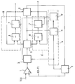
- FIG. 1 shows the block diagram of an ADC which works according to this method and makes both complex partial signals available for a downstream evaluation processor.
- the analog output signal of a slow, high-precision digital-to-analog converter 2 is added to the input signal Y in an adder 1 and the remaining analog sum signal is converted into a digital value in a fast A / D converter 3.
- a switch 5 switched by a control unit 4, which switches the output of the A / D converter 3 alternately with the arithmetic unit 8 formed from the subtractor 6 and the buffer store 7 and with that from a further subtractor 6 'and an intermediate memory 7' formed arithmetic unit 8 '.
- the outputs of these arithmetic units 8 and 8 ' are alternately connected to the input of the digital-to-analog converter 2 in synchronism with the switch 5 by a second switch 9.
- the output signals of the two arithmetic units 8 and 8 ' are passed directly to the assigned inputs of the digital low-pass filters 10, 10'.
- the output signal of the low-pass filter is available for further use in the system.
- the internal operating cycle of the arithmetic units 8 and 8 'as well as that of the A / D converter 3 is large compared to the converter cycle and is determined by the clock generator 12 in the control unit 4.
- ADC 3 receives a "walk" request.
- DAC 2 converts. After expiry of Periods of the wearer related to the last A / D conversion is the next request "convert" to ADC 3 7 and 7 'and 6 and 6' swap roles, etc.
- B the current frequency deviation 75 kHz and the sampling / carrier frequency 10.7 MHz and should have the dynamic range 20 dB and the baseband signal 60 dB S / N, so taking into account the gain in S / N for the baseband signal by the conversion
Landscapes
- Engineering & Computer Science (AREA)
- Theoretical Computer Science (AREA)
- Analogue/Digital Conversion (AREA)
Applications Claiming Priority (3)
| Application Number | Priority Date | Filing Date | Title |
|---|---|---|---|
| DE4219841A DE4219841A1 (de) | 1992-06-17 | 1992-06-17 | Verfahren zur Analog-Digital-Wandlung |
| DE4219841 | 1992-06-17 | ||
| US08/074,333 US5317313A (en) | 1992-06-17 | 1993-06-09 | Method and apparatus for analog/digital conversion |
Publications (2)
| Publication Number | Publication Date |
|---|---|
| EP0574812A2 true EP0574812A2 (fr) | 1993-12-22 |
| EP0574812A3 EP0574812A3 (fr) | 1997-12-17 |
Family
ID=25915789
Family Applications (1)
| Application Number | Title | Priority Date | Filing Date |
|---|---|---|---|
| EP93109208A Withdrawn EP0574812A3 (fr) | 1992-06-17 | 1993-06-08 | Procédé de conversion analogique-numérique |
Country Status (4)
| Country | Link |
|---|---|
| US (1) | US5317313A (fr) |
| EP (1) | EP0574812A3 (fr) |
| JP (1) | JPH0685674A (fr) |
| DE (1) | DE4219841A1 (fr) |
Families Citing this family (3)
| Publication number | Priority date | Publication date | Assignee | Title |
|---|---|---|---|---|
| EP0256502A3 (fr) * | 1986-08-15 | 1989-09-27 | Kabushiki Kaisha Toshiba | Appareil de formation d'images ayant une fonction de formation d'une marque de mise en place |
| US4878110A (en) * | 1986-08-15 | 1989-10-31 | Konishiroku Photo Industry Co., Ltd. | Color image processing apparatus which accurately registers multiple color images by counting pulses from a timer reset by a drum index signal |
| TW341415U (en) * | 1997-04-08 | 1998-09-21 | United Microelectronics Corp | A digital data cutting circuit |
Family Cites Families (5)
| Publication number | Priority date | Publication date | Assignee | Title |
|---|---|---|---|---|
| US4204198A (en) * | 1977-12-20 | 1980-05-20 | The United States Of America As Represented By The Secretary Of The Army | Radar analog to digital converter |
| US4737728A (en) * | 1986-02-28 | 1988-04-12 | Hitachi, Ltd. | Digitally processed demodulator for quadrature modulated signals |
| KR890003136A (ko) * | 1987-07-22 | 1989-04-13 | 강진구 | 전병렬 축차 비교형 아날로그-디지탈 변환기 |
| JP3011424B2 (ja) * | 1990-01-24 | 2000-02-21 | 株式会社東芝 | A/d変換器 |
| US5241312A (en) * | 1992-03-09 | 1993-08-31 | Long Christopher R | High resolution analog to digital converter |
-
1992
- 1992-06-17 DE DE4219841A patent/DE4219841A1/de not_active Withdrawn
-
1993
- 1993-06-08 EP EP93109208A patent/EP0574812A3/fr not_active Withdrawn
- 1993-06-09 US US08/074,333 patent/US5317313A/en not_active Expired - Fee Related
- 1993-06-16 JP JP5144891A patent/JPH0685674A/ja active Pending
Also Published As
| Publication number | Publication date |
|---|---|
| US5317313A (en) | 1994-05-31 |
| DE4219841A1 (de) | 1993-12-23 |
| EP0574812A3 (fr) | 1997-12-17 |
| JPH0685674A (ja) | 1994-03-25 |
Similar Documents
| Publication | Publication Date | Title |
|---|---|---|
| EP0080014B1 (fr) | Démodulateur numérique pour signaux modulés en fréquence | |
| EP0344467B1 (fr) | Récepteur à signaux en quadrature | |
| DE69413548T2 (de) | Verbessertes rom filter | |
| DE69635573T2 (de) | Frequenzsynthetisierer | |
| DE69004770T2 (de) | Frequenzmodulator. | |
| EP0074597A2 (fr) | Procédé et dispositif pour le réglage numérique de la phase du signal d'horloge d'un système numérique de traitement de signal | |
| DE3688170T2 (de) | Digitale zero-mf selektive stufe. | |
| DE3938126A1 (de) | Empfaenger mit direkter quadratur-abtastung des eingangssignals | |
| EP0210292A1 (fr) | Circuit de démodulation de fréquence avec comptage des passages par zéro | |
| WO1986005594A1 (fr) | Circuit d'obtention d'une valeur moyenne | |
| EP0421395A2 (fr) | Agencement de conversion d'une grandeur électrique d'entrée en un signal électrique continu proportionnel à ladite grandeur | |
| EP0091570A1 (fr) | Démodulateur numérique | |
| DE3841388C2 (fr) | ||
| DE4219841A1 (de) | Verfahren zur Analog-Digital-Wandlung | |
| DE3919530A1 (de) | Verfahren zur digitalen modulation und digitaler modulator | |
| DE3433592C2 (fr) | ||
| EP0068579B1 (fr) | Montage pour la démodulation d'un signal d'entrée modulé en fréquence | |
| DE3943072C2 (fr) | ||
| EP0148528B1 (fr) | Méthode et circuit pour augmenter la résolution d'un signal digital dépendant du temps | |
| DE2831734C3 (de) | Signalgenerator zur Erzeugung sinusförmiger Ausgangssignale mit vorbestimmter gegenseitiger Phasenlage | |
| DE19819069A1 (de) | Schaltungsanordnung zur arithmetischen Verknüpfung eines Analogsignals mit einem in digitaler Form vorliegenden Wert sowie Verfahren und Schaltungsanordnung zur Bestimmung eines Winkels | |
| CH647112A5 (de) | Schaltungsanordnung zur gewinnung einer zu der impulsdichte einer impulsfolge proportionalen steuerspannung. | |
| DE4022387C2 (fr) | ||
| DE69413633T2 (de) | Methode und Vorrichtung zur Abtastung von elektrischen Signalen | |
| DE2260264C3 (de) | Verfahren und Anordnung zur Schätzwertbildung in einem Codierer für Differenz-Pulscodemodulation |
Legal Events
| Date | Code | Title | Description |
|---|---|---|---|
| PUAI | Public reference made under article 153(3) epc to a published international application that has entered the european phase |
Free format text: ORIGINAL CODE: 0009012 |
|
| AK | Designated contracting states |
Kind code of ref document: A2 Designated state(s): AT CH DE ES FR GB IT LI NL |
|
| PUAL | Search report despatched |
Free format text: ORIGINAL CODE: 0009013 |
|
| AK | Designated contracting states |
Kind code of ref document: A3 Designated state(s): AT CH DE ES FR GB IT LI NL |
|
| STAA | Information on the status of an ep patent application or granted ep patent |
Free format text: STATUS: THE APPLICATION IS DEEMED TO BE WITHDRAWN |
|
| 18D | Application deemed to be withdrawn |
Effective date: 19980519 |