EP0574816A1 - Laservorspannungs- und -modulationsschaltung - Google Patents
Laservorspannungs- und -modulationsschaltung Download PDFInfo
- Publication number
- EP0574816A1 EP0574816A1 EP93109253A EP93109253A EP0574816A1 EP 0574816 A1 EP0574816 A1 EP 0574816A1 EP 93109253 A EP93109253 A EP 93109253A EP 93109253 A EP93109253 A EP 93109253A EP 0574816 A1 EP0574816 A1 EP 0574816A1
- Authority
- EP
- European Patent Office
- Prior art keywords
- signal
- providing
- responsive
- sensed
- laser
- Prior art date
- Legal status (The legal status is an assumption and is not a legal conclusion. Google has not performed a legal analysis and makes no representation as to the accuracy of the status listed.)
- Granted
Links
- 238000000034 method Methods 0.000 claims description 8
- 238000001514 detection method Methods 0.000 claims description 6
- 230000004044 response Effects 0.000 claims description 6
- 238000006243 chemical reaction Methods 0.000 claims description 4
- 238000012544 monitoring process Methods 0.000 claims 2
- 239000003990 capacitor Substances 0.000 description 9
- 230000003287 optical effect Effects 0.000 description 6
- 239000000872 buffer Substances 0.000 description 5
- 230000000694 effects Effects 0.000 description 5
- 239000013307 optical fiber Substances 0.000 description 5
- 230000007704 transition Effects 0.000 description 5
- 230000005540 biological transmission Effects 0.000 description 4
- 230000008901 benefit Effects 0.000 description 2
- 230000008859 change Effects 0.000 description 2
- 230000001276 controlling effect Effects 0.000 description 2
- 230000001419 dependent effect Effects 0.000 description 2
- 239000000835 fiber Substances 0.000 description 2
- 230000001105 regulatory effect Effects 0.000 description 2
- 230000002238 attenuated effect Effects 0.000 description 1
- 238000012512 characterization method Methods 0.000 description 1
- 239000002131 composite material Substances 0.000 description 1
- 230000003750 conditioning effect Effects 0.000 description 1
- 238000001816 cooling Methods 0.000 description 1
- 230000008878 coupling Effects 0.000 description 1
- 238000010168 coupling process Methods 0.000 description 1
- 238000005859 coupling reaction Methods 0.000 description 1
- 230000007423 decrease Effects 0.000 description 1
- 230000003247 decreasing effect Effects 0.000 description 1
- 238000010586 diagram Methods 0.000 description 1
- 238000001228 spectrum Methods 0.000 description 1
Images


Classifications
-
- H—ELECTRICITY
- H01—ELECTRIC ELEMENTS
- H01S—DEVICES USING THE PROCESS OF LIGHT AMPLIFICATION BY STIMULATED EMISSION OF RADIATION [LASER] TO AMPLIFY OR GENERATE LIGHT; DEVICES USING STIMULATED EMISSION OF ELECTROMAGNETIC RADIATION IN WAVE RANGES OTHER THAN OPTICAL
- H01S5/00—Semiconductor lasers
- H01S5/06—Arrangements for controlling the laser output parameters, e.g. by operating on the active medium
- H01S5/068—Stabilisation of laser output parameters
- H01S5/0683—Stabilisation of laser output parameters by monitoring the optical output parameters
- H01S5/06832—Stabilising during amplitude modulation
Definitions
- This invention relates to the transmission of information on optical fibers and, more particularly, to a control circuit for controlling a laser for providing optical signals to an optical fiber.
- Laser diodes are commonly used to provide optical signals to optical fibers for transmission thereon.
- the laser diode will be biased at some selected bias current level, and the diode will then be intensity-modulated about that bias point at a modulation level necessary to achieve a desired light output level.
- the lasing threshold tends to increase with increasing temperature. This implies that, to maintain a constant average optical output power with an increase in temperature, average drive current, often called bias current, must be increased.
- bias current often called bias current
- the efficiency of the laser current-to-optical power conversion decreases with increasing temperature.
- the slope efficiency decreasing with increasing temperature is the same as the first: to maintain at a constant average optical output power with increasing temperature, bias current must be increased.
- Another implication of the second effect is that, to maintain a constant signal , or modulation, optical output power with increasing temperature, modulation current must be increased.
- thermo-electric cooling to maintain the laser at a relatively constant temperature.
- This solution is generally costly, power consumptive, and usually unacceptable for high-volume, low-cost applications.
- Another possible solution has been to simply monitor the laser temperature and adjust the bias and signal current levels according to expected performance curves.
- the change in characteristics with temperature is usually not accurately predictable from device to device. This mandates that either each laser be individually characterized over temperature, or that a feedback loop be established to control the laser in operation. Individual characterization, besides being expensive, has the additional disadvantage of not accounting for any changes in laser characteristics that may occur as the laser ages.
- a feedback loop can be established through the laser's own back facet monitor photodiode, or through the whole link and the receiver at the opposite end.
- the latter approach has the advantage of being able to accommodate changes in the cable plant, the receiver, and the laser-to-fiber coupling. It has the disadvantage of requiring the addition of control circuitry at the receiver and a link back to the transmitter. If the feedback link is already present link capacity may be used for feedback information. However, the possibility that feedback information may not arrive back to the laser in a timely fashion, causing instability in the laser performance, must also be considered.
- the object of the present invention is to regulate a laser.
- constant light output from a laser diode over various temperatures is achieved by adjusting the bias current in accordance with a first set of parameters and adjusting the modulation current amplitude in accordance with a second set of parameters.
- constant light output over various modulation coding schemes from a laser diode is achieved by adjusting the bias current in accordance with a first set of parameters and adjusting the modulation current amplitude in accordance with a second set of parameters.
- the first set of parameters may comprise an average of detected peak and valley amplitudes of the light output from the laser diode.
- the second set of parameters may comprise a difference between the peak and valley of the light output from the laser diode.
- This invention was first conceived as a way to regulate a low-cost, uncooled laser, which was intended to be modulated with a frequency multiplexed hybrid signal consisting of a relatively low speed (less than 50 megabaud) digital signal and a high-speed (up to 1 gigahertz) analog composite video signal.
- the application for the invention was in a fiber-to-the-curb system, where wide temperature ranges must be handled by low-cost designs, and where the transmitted signal is a hybrid analog video/digital voice signal.
- the present invention provides a way to use the already-present digital signal in an all-digital or all-hybrid digital/analog application as a virtual pilot.
- Fig. 1 shows that a constant output power may be achieved for varying efficiencies or operating points of a laser diode modulated by a modulating signal by controlling the bias point and the amplitude of the modulation.
- the present invention automatically compensates by varying the operating point and the amplitude of modulation. This is shown for three different temperatures, resulting in three different operating points and amplitudes of the modulating signal.
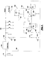
- Fig. 2 shows an embodiment of the present invention which includes a feedback circuit 10 used to regulate a low-cost, uncooled laser 12, which is being modulated by a frequency-division multiplexed signal 14 which is shown before being multiplexed within a driver 20 as two separate signals on a pair of lines 16, 18.
- the components 16, 18 of the signal 14 may comprise a relatively low-speed digital data signal (for example, at less than 50 megabaud) and one or more high-speed RF signals such as analog television channels (spaced along the frequency spectrum up to 1 gigahertz, for example).
- the laser driver circuit 20 is responsive to the signals on the lines 16, 18, multiplexes the signals 16, 18 into the frequency-division multiplexed signal 14 and provides drive current for the laser 12, which in turn provides light output 22 to an optical fiber (not shown) for transmission thereon.
- the laser driver modulates the laser around a bias current level and transmits light 22 into the optical fiber through its front facet and also transmits light 24 into a monitor photodiode 26 through its back facet.
- the frequency response of the monitor diode is generally slow enough to block the analog video signals, but fast enough to pass the digital signal. However, if the analog video signals are not significantly attenuated at the monitor diode, then a lowpass filter 28 may be inserted in the signal path to filter them out.
- either the laser back facet monitor diode 26 or the lowpass filter, or both, will provide a filtered low-frequency signal on a line 30 to a current-to-voltage level converter 32, which may be nothing more than a resistor network to a reference to provide a voltage on the same line 30 to a voltage peak-to-peak detector 36a, 36b.
- the response and hold times of the peak and valley detectors are set depending upon the symbol rate of the digital data and the longest duration between transitions. It should be realized that true non-return-to-zero (NRZ) encoding, where the time between symbol transitions can be extremely long, cannot be used with the embodiment disclosed herein.
- NRZ non-return-to-zero
- the control voltages on the lines 38a, 38b are provided to an averager 40 and a difference detector 42.
- the peak and valley voltages 38a, 38b are averaged to find the midpoint, and a midpoint signal having a magnitude indicative thereof is provided on a line 44 to a laser bias control 46. Because peak and valley voltages are used to determine the midpoint, instead of performing average level detection immediately after the back facet monitor, data and coding scheme dependent wandering of the average level is avoided. If the coding scheme utilized does not have a true 50 percent effective duty cycle where one is guaranteed a transition in data and between bits, any variations that would otherwise be caused in laser bias control due to variations away from 50 percent duty cycle are avoided.
- the midpoint voltage on the line 44 is provided to the laser bias control block 46, where it is compared to a threshold signal on a line 48 which may be adjustable, as indicated by a threshold adjust block 50.
- the threshold is chosen to place the laser at a selected average optical output power level,such as the P0 level shown in Fig. 1. If the midpoint voltage is below the threshold, then the laser bias control block provides a signal on a line 52 to increase the bias current in the laser driver block 20 until the midpoint voltage equals the threshold. An opposite effect occurs if the midpoint voltage is above threshold.
- the difference between the peak and valley voltages on the lines 38a, 38b, respectively is determined.
- a difference voltage signal is provided on a line 54 to a laser modulation control block 56, where it is compared to a threshold signal on a line 58 provided by a threshold adjust block 60 which may be capable of adjusting the level of the threshold reference signal on the line 58.
- the threshold is set according to the desired modulation index or ratio of signal-power-to-average-power out of the laser of the digital signal. If the difference voltage is below threshold, then the laser modulation control block provides a signal on a line 62 to increase the gain of the signal in the laser driver 20. An opposite effect occurs if the difference voltage is above threshold. In the driver, both the digital and analog signals are adjusted proportionately, so that the relative modulation indices set up for the two signal types is maintained.
- Fig. 3 a detailed illustration is shown of one way to construct a digital portion of the laser driver 20 of Fig. 2 for handling the relatively low-speed digital data input signal on the line 16. That signal is first terminated by a resistor 70 and capacitor 72 in parallel, which helps with proper switching of a transistor 74 to prevent pulsewidth distortion.
- the transistor 74 is sourced by a VCC voltage at a node 76 at +5V.
- the collector voltage is filtered by a capacitor pair 78 in parallel, and a series of resistors 79 is employed for the purpose of level conversion before being buffered by a buffer stage 80, which also serves to convert the driving signal to a driving signal having negative excursions. This was done for the particular embodiment shown because of the particular laser selected, which needs to be driven negatively. This, of course, need not be the case.
- An emitter follower section 82 follows the buffer stage 80 and further level converts the input to get closer to a negative 5V suited to the particular laser diode 12 we selected.
- a buffer section 84 buffers the output of the emitter follower section 82 and is itself followed by a lowpass filter section 86 which passes signals, for example in the range of 0-20 MHz. This is not the same as the lowpass filter 28 shown in Fig. 2, but is merely provided to eliminate higher frequency components from the digital signal which would otherwise cause distortions in the analog video signal, to be multiplexed with the digital at node 102.
- the lowpass filter 86 is followed by a further conversion section 88 which places the most negative excursion of the filtered signal almost down to -5V so that a minimal DC current will be provided by this section.
- the resistor 91 sets the modulation current for the digital signal in the laser 12.
- the light output 24 from the laser diode 12 is detected by the back facet 26 thereof, and the detected signal is provided on the line 30, as described above in connection with Fig. 2.
- a lowpass filter 28 is shown in Fig. 2, for the particular case illustrated, it was found not necessary to include such a lowpass filter, since the capacitance of the diode itself plus the input resistance of the transistor 154 circuit was sufficiently great to provide an effective lowpass filter, in this particular case.
- Fig. 4 In connection with the description of Fig. 4 below, it will be seen that the output thereof is provided on a line 100 to a summing node 102 shown in Fig. 3, where the output of the video circuit of Fig. 4 is summed with the current contributed by the digital portion illustrated in Fig. 3.
- the multiplexed signal thus modulates the diode 12.
- FIG. 4 an illustration is shown of video circuitry for a laser driver 20 embodiment, according to the present invention.
- the high-speed RF signals 18 of Fig. 2 are shown at the upper left of Fig. 4 as an input signal to a voltage controlled attenuator 104 to keep the video level at a constant level as controlled by a signal on a line 106, which is in turn controlled by the feedback signal on the line 62 shown in both Fig. 2 and Fig. 4 (from the laser modulation control 56 to be disclosed in more detail below in connection with Fig. 5).
- An output signal on a line 106 from the voltage controlled attenuator 104 is filtered by a highpass filter 108 for getting rid of any low frequency components that might otherwise corrupt the digital signals to be joined with the video signals on the line 100, as shown summed at the junction 102 in Fig. 3.
- the signal on the line 106 is also provided to a series of resistors 109, 110 and a capacitor 112, which together serve the purpose of presenting an impedance which prevents any influence of the control circuitry on the video signal path 106.
- resistors 109, 110 and the capacitor 112 have values selected such that the impedance presented to the main line 106 is greater than ten times the characteristic impedance of the main line 106.
- a diode 114 (configured as a back diode to minimize temperature drift effects) and capacitor 116 serve the purpose of doing average power detection.
- the capacitor 116 also acts in concert with a resistor 118 as a pre-integrator to prevent instantaneous high peaks from being presented to an integrator 120 which integrates a signal on a line 122, to provide an integrated output signal on a line 124.
- the integrator is with reference to a reference signal on a line 126, whereby the integrator 120 tries to zero the difference between the signal on the line 122 and the signal on the line 126.
- stages 128, 130 perform both gain and level shifting by moving the DC swing of a signal on line 132 into a range that the voltage-controlled attenuator 104 needs as a control voltage, i.e., between 0 and -5V.
- the differential amplifier stage 130 drives the difference between the input signal on the line 132 and an input signal on a line 134 to zero.
- the signal on the line 134 is provided by a signal conditioning stage 136 responsive to the feedback signal on the line 62 from Fig. 5.
- Fig. 5 shows the laser bias and AGC control part of Fig. 2.
- a voltage regulator 150 is responsive to the -5V on line 92 for providing a regulated -2.5V on a line 152. At equilibrium, the voltage on the line 34 sits at -1.25V, and the amount of swing is determined by the way the modulation index is set up.
- a transistor 154 is responsive at its collector to the +5V on the line 76 and provides a current through a pair of resistors 156, 158, which have a connecting node 160 which, at equilibrium, sits at -2.5V.
- the peak detector 36a and valley detector 36b of Fig. 2 are shown in one embodiment in Fig. 5.
- a buffer operational amplifier 162 provides the captured peak signal on the line 38a, which is held by a circuit 164 having a resistor 166 and a capacitor 168 with values chosen so as to have a time constant longer than the longest expected time between transitions of the digital input signal, which may be unbalanced in the sense of not having a 50 percent duty cycle.
- the resistive value may be chosen to be 162 Kohm, while the capacitor may be about 33 picofarad. Similar values can be chosen for a resistor 170 and a capacitor 172 in a circuit 174 having a purpose of holding the peak or valley of the signal on the line 160.
- An operational amplifier 176 provides the valley signal on the line 38b to the averager 40, which is responsive to both the signal on the line 38b and to the signal on the line 38a for finding the midpoint.
- a differential amplifier 180 compares the reference signal on the line 48 to the average signal on the line 44, as previously discussed in connection with Fig. 2. The output of the differential amplifier 180 is the signal on the line 52 shown in Fig.
- a feedback signal for the laser driver is used to drive a transistor 181.
- a DC or bias current is set by resistor 181a and is then summed through line 182 at node 102 with the video and digital modulation currents passing through the laser diode 12.
- the signal on the line 38a is a signal representing the latest peak value of the input signal. It is provided not only to the voltage follower 40 of the average detector, but also the difference detector 42 which is responsive also to the signal on the line 38b for providing the difference signal on the line 54 to a comparator 190, which compares the difference signal on the line 54 to the reference signal on the line 58 and provides the feedback signal on the line 62 to the video portion of the laser driver, as shown in Fig. 4.
- the signal on the line 62 is also used at the gate of an FET 192 used as a voltage-controlled resistor in the digital portion of the laser driver circuit of Fig. 3. The signal changes the resistance of the FET in accordance with changes in the difference in the peak and valley, therefore changing the voltage division ration of the digital signal after transistor 80 in Fig 3.
Landscapes
- Physics & Mathematics (AREA)
- Condensed Matter Physics & Semiconductors (AREA)
- General Physics & Mathematics (AREA)
- Electromagnetism (AREA)
- Optics & Photonics (AREA)
- Semiconductor Lasers (AREA)
Applications Claiming Priority (2)
| Application Number | Priority Date | Filing Date | Title |
|---|---|---|---|
| US07/898,702 US5268916A (en) | 1992-06-15 | 1992-06-15 | Laser bias and modulation circuit |
| US898702 | 1992-06-15 |
Publications (2)
| Publication Number | Publication Date |
|---|---|
| EP0574816A1 true EP0574816A1 (de) | 1993-12-22 |
| EP0574816B1 EP0574816B1 (de) | 1996-09-18 |
Family
ID=25409914
Family Applications (1)
| Application Number | Title | Priority Date | Filing Date |
|---|---|---|---|
| EP93109253A Expired - Lifetime EP0574816B1 (de) | 1992-06-15 | 1993-06-09 | Laservorspannungs- und -modulationsschaltung |
Country Status (7)
| Country | Link |
|---|---|
| US (2) | US5268916A (de) |
| EP (1) | EP0574816B1 (de) |
| JP (1) | JPH0685363A (de) |
| AT (1) | ATE143184T1 (de) |
| CA (1) | CA2098343A1 (de) |
| DE (1) | DE69304806T2 (de) |
| ES (1) | ES2094415T3 (de) |
Cited By (4)
| Publication number | Priority date | Publication date | Assignee | Title |
|---|---|---|---|---|
| EP0662740A3 (de) * | 1994-01-05 | 1996-01-03 | Alcatel Nv | Vorrichtung und Verfahren zur Kontrolle von Strom und Modulation eines Lasers. |
| WO2003023917A1 (en) * | 2001-09-07 | 2003-03-20 | Optillion Ab | Laser modulation control |
| WO2011041996A1 (de) * | 2009-10-09 | 2011-04-14 | Bktel Communications Gmbh | Verfahren und vorrichtung zur optischen übertragung eines wechselstromsignals |
| WO2023046578A1 (en) | 2021-09-21 | 2023-03-30 | Signify Holding B.V. | An optical wireless communication system |
Families Citing this family (35)
| Publication number | Priority date | Publication date | Assignee | Title |
|---|---|---|---|---|
| US5268916A (en) * | 1992-06-15 | 1993-12-07 | Alcatel Network Systems, Inc. | Laser bias and modulation circuit |
| JPH0795160A (ja) * | 1993-09-20 | 1995-04-07 | Fujitsu Ltd | 光増幅器の応答信号変調方法 |
| US5408485A (en) * | 1994-05-11 | 1995-04-18 | Alcatel Network Systems, Inc. | Laser modulation controller using NRZ electrical modulation level control |
| US5726437A (en) * | 1994-10-27 | 1998-03-10 | Fuji Xerox Co., Ltd. | Light intensity control device |
| US5541759A (en) * | 1995-05-09 | 1996-07-30 | Microsym Computers, Inc. | Single fiber transceiver and network |
| US5953690A (en) * | 1996-07-01 | 1999-09-14 | Pacific Fiberoptics, Inc. | Intelligent fiberoptic receivers and method of operating and manufacturing the same |
| US5812572A (en) * | 1996-07-01 | 1998-09-22 | Pacific Fiberoptics, Inc. | Intelligent fiberoptic transmitters and methods of operating and manufacturing the same |
| US5963570A (en) * | 1997-05-12 | 1999-10-05 | At&T Corp. | Current control for an analog optical link |
| US6208686B1 (en) * | 1997-07-18 | 2001-03-27 | Innova Corporation | System and method for dynamic amplitude adjustment of modulating signal in frequency modulated transceivers |
| US6229833B1 (en) * | 1997-10-16 | 2001-05-08 | Fujitsu Limited | Laser diode protecting circuit and laser driving current control circuit |
| DE69820393T2 (de) * | 1997-10-28 | 2004-10-07 | Broadband Royalty Corp | Optischer Sender zur Rauschimpulsverringerung in einer faseroptischen Verbindung |
| US6137522A (en) * | 1998-01-07 | 2000-10-24 | Xerox Corporation | Raster output scanner exposure control for bias and run levels in a multiple diode system |
| JP3085274B2 (ja) * | 1998-01-19 | 2000-09-04 | 日本電気株式会社 | 光送信器 |
| US6049073A (en) * | 1998-03-27 | 2000-04-11 | Eastman Kodak Company | Control circuit for a stabilized laser |
| JPH11344689A (ja) * | 1998-06-03 | 1999-12-14 | Hitachi Ltd | 固体レーザ装置 |
| US6549310B1 (en) | 1999-01-08 | 2003-04-15 | International Business Machines Corporation | Fiber optic data link module with built-in link diagnostics |
| US7181146B1 (en) | 2001-01-17 | 2007-02-20 | Optical Communication Products, Inc. | Self-adjusting data transmitter |
| US6560258B1 (en) | 2001-04-17 | 2003-05-06 | Analog Devices, Inc. | Direct-coupled laser diode driver structures and methods |
| DE50105000D1 (de) * | 2001-08-03 | 2005-02-03 | Infineon Technologies Ag | Verfahren und vorrichtung zur regelung eines lasers |
| US7212747B2 (en) * | 2002-06-10 | 2007-05-01 | Matsushita Electric Industrial Co., Ltd. | Optical transmission device and optical transmission method for transmitting a burst radio signal |
| US6941080B2 (en) | 2002-07-15 | 2005-09-06 | Triquint Technology Holding Co. | Method and apparatus for directly modulating a laser diode using multi-stage driver circuitry |
| JP4205916B2 (ja) * | 2002-09-03 | 2009-01-07 | パナソニック株式会社 | 消光比補償レーザ駆動回路及び光通信装置 |
| US6928094B2 (en) * | 2002-12-16 | 2005-08-09 | Intel Corporation | Laser driver circuit and system |
| ATE424640T1 (de) | 2003-01-08 | 2009-03-15 | Tecey Software Dev Kg Llc | Vorrichtung und verfahren zur messung dynamischer lasersignale |
| US7142574B2 (en) * | 2003-05-21 | 2006-11-28 | Intel Corporation | Laser driver circuit and system |
| US7027685B2 (en) * | 2003-08-20 | 2006-04-11 | The Boeing Company | Apparatus and method for fiber optic link with built-in test |
| US7418015B2 (en) * | 2004-02-23 | 2008-08-26 | Finisar Corporation | System and method for control of optical transmitter |
| ATE489750T1 (de) * | 2004-04-21 | 2010-12-15 | Tecey Software Dev Kg Llc | Verfahren und vorrichtung für durch digitale signalverarbeitung verbesserte kompensation der laser-leistungsfähigkeit |
| JP2005317666A (ja) * | 2004-04-27 | 2005-11-10 | Sumitomo Electric Ind Ltd | レーザ駆動回路 |
| US20050271100A1 (en) * | 2004-06-04 | 2005-12-08 | Keith Everett | System and method for controlling optical sources, such as laser diodes, and computer program product therefor |
| US7505692B2 (en) * | 2004-08-31 | 2009-03-17 | Cisco Technology, Inc. | System and method for optical transmission |
| TWI287340B (en) * | 2004-12-07 | 2007-09-21 | Ind Tech Res Inst | Laser driver with automatic power control |
| US7639001B2 (en) * | 2006-01-17 | 2009-12-29 | The Boeing Company | Built-in test for high speed electrical networks |
| JP4973005B2 (ja) | 2006-05-24 | 2012-07-11 | 日立電線株式会社 | レーザ制御装置及びその制御方法 |
| CN115347453B (zh) * | 2021-05-12 | 2026-01-06 | 上海禾赛科技有限公司 | 激光发射控制电路、激光雷达及激光器温漂控制方法 |
Citations (4)
| Publication number | Priority date | Publication date | Assignee | Title |
|---|---|---|---|---|
| GB2066557A (en) * | 1979-12-27 | 1981-07-08 | Western Electric Co | Injection laser output stabilisation |
| GB2074311A (en) * | 1980-02-25 | 1981-10-28 | Western Electric Co | Digital laser transmitter |
| EP0052536A1 (de) * | 1980-11-14 | 1982-05-26 | Lignes Telegraphiques Et Telephoniques L.T.T. | Sendermodul-Ausgangsleistungsstabilisierungsanordnung für ein Lichtwellenleiter-Übertragungssystem |
| US4355395A (en) * | 1978-04-10 | 1982-10-19 | British Telecommunications | Injection lasers |
Family Cites Families (8)
| Publication number | Priority date | Publication date | Assignee | Title |
|---|---|---|---|---|
| DE2841433C2 (de) * | 1978-09-22 | 1983-08-25 | Siemens Ag, 1000 Berlin Und 8000 Muenchen | Vorstromregelung von Laserdioden |
| JPS6245086A (ja) * | 1985-08-22 | 1987-02-27 | Oki Electric Ind Co Ltd | レ−ザダイオ−ド駆動回路 |
| EP0347202A3 (de) * | 1988-06-14 | 1991-03-20 | Brother Kogyo Kabushiki Kaisha | Anregungssystem für Halbleiter-Laservorrichtung |
| JP2706262B2 (ja) * | 1988-07-12 | 1998-01-28 | キヤノン株式会社 | 半導体レーザ駆動装置 |
| JP2612608B2 (ja) * | 1988-10-20 | 1997-05-21 | キヤノン株式会社 | 半導体レーザ駆動装置 |
| US5018154A (en) * | 1989-09-12 | 1991-05-21 | Brother Kogyo Kabushiki Kaisha | Semiconductor laser drive device |
| JPH03216363A (ja) * | 1990-01-22 | 1991-09-24 | Fuji Photo Film Co Ltd | 半導体レーザの駆動装置 |
| US5268916A (en) * | 1992-06-15 | 1993-12-07 | Alcatel Network Systems, Inc. | Laser bias and modulation circuit |
-
1992
- 1992-06-15 US US07/898,702 patent/US5268916A/en not_active Expired - Fee Related
-
1993
- 1993-06-09 EP EP93109253A patent/EP0574816B1/de not_active Expired - Lifetime
- 1993-06-09 DE DE69304806T patent/DE69304806T2/de not_active Expired - Lifetime
- 1993-06-09 ES ES93109253T patent/ES2094415T3/es not_active Expired - Lifetime
- 1993-06-09 AT AT93109253T patent/ATE143184T1/de not_active IP Right Cessation
- 1993-06-14 CA CA002098343A patent/CA2098343A1/en not_active Abandoned
- 1993-06-15 JP JP5144030A patent/JPH0685363A/ja active Pending
- 1993-11-24 US US08/158,166 patent/US5488621A/en not_active Expired - Lifetime
Patent Citations (4)
| Publication number | Priority date | Publication date | Assignee | Title |
|---|---|---|---|---|
| US4355395A (en) * | 1978-04-10 | 1982-10-19 | British Telecommunications | Injection lasers |
| GB2066557A (en) * | 1979-12-27 | 1981-07-08 | Western Electric Co | Injection laser output stabilisation |
| GB2074311A (en) * | 1980-02-25 | 1981-10-28 | Western Electric Co | Digital laser transmitter |
| EP0052536A1 (de) * | 1980-11-14 | 1982-05-26 | Lignes Telegraphiques Et Telephoniques L.T.T. | Sendermodul-Ausgangsleistungsstabilisierungsanordnung für ein Lichtwellenleiter-Übertragungssystem |
Non-Patent Citations (3)
| Title |
|---|
| BELL SYSTEM TECHNICAL JOURNAL vol. 62, no. 7, September 1983, MURRAY HILL, US pages 1923 - 1936 R.G. SWARTZ, B.A. WOOLEY 'Stabilized Biasing of Semiconductor Lasers' * |
| PATENT ABSTRACTS OF JAPAN vol. 11, no. 227 (E-526)23 July 1987 & JP-A-62 045 086 ( OKI ELECTRIC ) 27 February 1987 * |
| PATENT ABSTRACTS OF JAPAN vol. 14, no. 328 (E-952)(4271) 13 July 1990 & JP-A-02 111 087 ( CANON ) 24 April 1990 * |
Cited By (4)
| Publication number | Priority date | Publication date | Assignee | Title |
|---|---|---|---|---|
| EP0662740A3 (de) * | 1994-01-05 | 1996-01-03 | Alcatel Nv | Vorrichtung und Verfahren zur Kontrolle von Strom und Modulation eines Lasers. |
| WO2003023917A1 (en) * | 2001-09-07 | 2003-03-20 | Optillion Ab | Laser modulation control |
| WO2011041996A1 (de) * | 2009-10-09 | 2011-04-14 | Bktel Communications Gmbh | Verfahren und vorrichtung zur optischen übertragung eines wechselstromsignals |
| WO2023046578A1 (en) | 2021-09-21 | 2023-03-30 | Signify Holding B.V. | An optical wireless communication system |
Also Published As
| Publication number | Publication date |
|---|---|
| US5268916A (en) | 1993-12-07 |
| EP0574816B1 (de) | 1996-09-18 |
| US5488621A (en) | 1996-01-30 |
| ATE143184T1 (de) | 1996-10-15 |
| CA2098343A1 (en) | 1993-12-16 |
| JPH0685363A (ja) | 1994-03-25 |
| DE69304806D1 (de) | 1996-10-24 |
| DE69304806T2 (de) | 1997-02-06 |
| ES2094415T3 (es) | 1997-01-16 |
Similar Documents
| Publication | Publication Date | Title |
|---|---|---|
| US5268916A (en) | Laser bias and modulation circuit | |
| US5311005A (en) | Optical transmitters | |
| CA1081801A (en) | Regenerator for an optical transmission system | |
| US5402433A (en) | Apparatus and method for laser bias and modulation control | |
| US5502298A (en) | Apparatus and method for controlling an extinction ratio of a laser diode over temperature | |
| EP0513002B1 (de) | Lasersteuerschaltung | |
| US4677632A (en) | Coupled loop controller for a laser transmitter | |
| US4796266A (en) | Laser driver circuit with dynamic bias | |
| EP1061618B1 (de) | Leistungskontrolliertes Wellenlängestabilisationssystem | |
| US4608542A (en) | Bandwidth controlled data amplifier | |
| US5187713A (en) | Nonlinear device control methods and apparatus | |
| JPH01117385A (ja) | 半導体レーザバイアス電流制御方式 | |
| EP0626106B1 (de) | Verfahren und gerät zur steuerung eines lasers | |
| KR100545589B1 (ko) | 레이저 다이오드의 특성 보상 장치 및 이를 구비한 광송신기 | |
| US4543664A (en) | Direct current coupled data transmission | |
| JP3802232B2 (ja) | 光受信器 | |
| US5293263A (en) | Electro-optical modulator which provides optical bias stabilization during operation | |
| WO1993013577A1 (en) | Apparatus and method for controlling an extinction ratio of a laser diode over temperature | |
| JP2001189699A (ja) | 光送信器 | |
| AU672188B2 (en) | Apparatus and method for controlling an extinction ratio of a laser diode over temperature | |
| JPH0738185A (ja) | 発光素子の駆動回路 | |
| FI106677B (fi) | Säätömenetelmä ja säätöpiiri laserdiodilähettimen säätämiseksi | |
| JPH05347587A (ja) | 光送信機 | |
| JPH0553078B2 (de) | ||
| WO1992017007A1 (en) | Method and control circuit for controlling a laser diode transmitter |
Legal Events
| Date | Code | Title | Description |
|---|---|---|---|
| PUAI | Public reference made under article 153(3) epc to a published international application that has entered the european phase |
Free format text: ORIGINAL CODE: 0009012 |
|
| AK | Designated contracting states |
Kind code of ref document: A1 Designated state(s): AT BE CH DE ES FR GB IT LI NL SE |
|
| 17P | Request for examination filed |
Effective date: 19940221 |
|
| 17Q | First examination report despatched |
Effective date: 19940920 |
|
| GRAH | Despatch of communication of intention to grant a patent |
Free format text: ORIGINAL CODE: EPIDOS IGRA |
|
| GRAH | Despatch of communication of intention to grant a patent |
Free format text: ORIGINAL CODE: EPIDOS IGRA |
|
| GRAA | (expected) grant |
Free format text: ORIGINAL CODE: 0009210 |
|
| AK | Designated contracting states |
Kind code of ref document: B1 Designated state(s): AT BE CH DE ES FR GB IT LI NL SE |
|
| REF | Corresponds to: |
Ref document number: 143184 Country of ref document: AT Date of ref document: 19961015 Kind code of ref document: T |
|
| REG | Reference to a national code |
Ref country code: CH Ref legal event code: NV Representative=s name: JUERG ULRICH C/O ALCATEL STR AG |
|
| REF | Corresponds to: |
Ref document number: 69304806 Country of ref document: DE Date of ref document: 19961024 |
|
| ITF | It: translation for a ep patent filed | ||
| ET | Fr: translation filed | ||
| REG | Reference to a national code |
Ref country code: ES Ref legal event code: FG2A Ref document number: 2094415 Country of ref document: ES Kind code of ref document: T3 |
|
| PLBE | No opposition filed within time limit |
Free format text: ORIGINAL CODE: 0009261 |
|
| STAA | Information on the status of an ep patent application or granted ep patent |
Free format text: STATUS: NO OPPOSITION FILED WITHIN TIME LIMIT |
|
| 26N | No opposition filed | ||
| PGFP | Annual fee paid to national office [announced via postgrant information from national office to epo] |
Ref country code: CH Payment date: 19990514 Year of fee payment: 7 |
|
| PGFP | Annual fee paid to national office [announced via postgrant information from national office to epo] |
Ref country code: AT Payment date: 19990521 Year of fee payment: 7 |
|
| PGFP | Annual fee paid to national office [announced via postgrant information from national office to epo] |
Ref country code: NL Payment date: 20000524 Year of fee payment: 8 |
|
| PGFP | Annual fee paid to national office [announced via postgrant information from national office to epo] |
Ref country code: BE Payment date: 20000605 Year of fee payment: 8 |
|
| PG25 | Lapsed in a contracting state [announced via postgrant information from national office to epo] |
Ref country code: AT Free format text: LAPSE BECAUSE OF NON-PAYMENT OF DUE FEES Effective date: 20000609 |
|
| PG25 | Lapsed in a contracting state [announced via postgrant information from national office to epo] |
Ref country code: LI Free format text: LAPSE BECAUSE OF NON-PAYMENT OF DUE FEES Effective date: 20000630 Ref country code: CH Free format text: LAPSE BECAUSE OF NON-PAYMENT OF DUE FEES Effective date: 20000630 |
|
| REG | Reference to a national code |
Ref country code: CH Ref legal event code: PL |
|
| PG25 | Lapsed in a contracting state [announced via postgrant information from national office to epo] |
Ref country code: BE Free format text: LAPSE BECAUSE OF NON-PAYMENT OF DUE FEES Effective date: 20010630 |
|
| BERE | Be: lapsed |
Owner name: ALCATEL N.V. Effective date: 20010630 |
|
| PG25 | Lapsed in a contracting state [announced via postgrant information from national office to epo] |
Ref country code: NL Free format text: LAPSE BECAUSE OF NON-PAYMENT OF DUE FEES Effective date: 20020101 |
|
| REG | Reference to a national code |
Ref country code: GB Ref legal event code: IF02 |
|
| NLV4 | Nl: lapsed or anulled due to non-payment of the annual fee |
Effective date: 20020101 |
|
| PGFP | Annual fee paid to national office [announced via postgrant information from national office to epo] |
Ref country code: SE Payment date: 20040616 Year of fee payment: 12 |
|
| PGFP | Annual fee paid to national office [announced via postgrant information from national office to epo] |
Ref country code: ES Payment date: 20040618 Year of fee payment: 12 |
|
| PG25 | Lapsed in a contracting state [announced via postgrant information from national office to epo] |
Ref country code: SE Free format text: LAPSE BECAUSE OF NON-PAYMENT OF DUE FEES Effective date: 20050610 Ref country code: ES Free format text: LAPSE BECAUSE OF NON-PAYMENT OF DUE FEES Effective date: 20050610 |
|
| EUG | Se: european patent has lapsed | ||
| PGFP | Annual fee paid to national office [announced via postgrant information from national office to epo] |
Ref country code: IT Payment date: 20060630 Year of fee payment: 14 |
|
| REG | Reference to a national code |
Ref country code: ES Ref legal event code: FD2A Effective date: 20050610 |
|
| PG25 | Lapsed in a contracting state [announced via postgrant information from national office to epo] |
Ref country code: IT Free format text: LAPSE BECAUSE OF NON-PAYMENT OF DUE FEES Effective date: 20070609 |
|
| PGFP | Annual fee paid to national office [announced via postgrant information from national office to epo] |
Ref country code: DE Payment date: 20120622 Year of fee payment: 20 |
|
| PGFP | Annual fee paid to national office [announced via postgrant information from national office to epo] |
Ref country code: FR Payment date: 20120705 Year of fee payment: 20 Ref country code: GB Payment date: 20120622 Year of fee payment: 20 |
|
| REG | Reference to a national code |
Ref country code: DE Ref legal event code: R071 Ref document number: 69304806 Country of ref document: DE |
|
| REG | Reference to a national code |
Ref country code: GB Ref legal event code: PE20 Expiry date: 20130608 |
|
| PG25 | Lapsed in a contracting state [announced via postgrant information from national office to epo] |
Ref country code: GB Free format text: LAPSE BECAUSE OF EXPIRATION OF PROTECTION Effective date: 20130608 Ref country code: DE Free format text: LAPSE BECAUSE OF EXPIRATION OF PROTECTION Effective date: 20130611 |
|
| REG | Reference to a national code |
Ref country code: FR Ref legal event code: TP Owner name: ALCATEL LUCENT, FR Effective date: 20130708 Ref country code: FR Ref legal event code: CD Owner name: ALCATEL LUCENT, FR Effective date: 20130708 |