EP0575280A2 - Transistor CMOS comportant une structure de porte inversée en tungstène comportant deux couches - Google Patents
Transistor CMOS comportant une structure de porte inversée en tungstène comportant deux couches Download PDFInfo
- Publication number
- EP0575280A2 EP0575280A2 EP93480057A EP93480057A EP0575280A2 EP 0575280 A2 EP0575280 A2 EP 0575280A2 EP 93480057 A EP93480057 A EP 93480057A EP 93480057 A EP93480057 A EP 93480057A EP 0575280 A2 EP0575280 A2 EP 0575280A2
- Authority
- EP
- European Patent Office
- Prior art keywords
- refractory metal
- layer
- mos transistor
- tungsten
- gate electrode
- Prior art date
- Legal status (The legal status is an assumption and is not a legal conclusion. Google has not performed a legal analysis and makes no representation as to the accuracy of the status listed.)
- Withdrawn
Links
Images

Classifications
-
- H—ELECTRICITY
- H10—SEMICONDUCTOR DEVICES; ELECTRIC SOLID-STATE DEVICES NOT OTHERWISE PROVIDED FOR
- H10D—INORGANIC ELECTRIC SEMICONDUCTOR DEVICES
- H10D30/00—Field-effect transistors [FET]
- H10D30/01—Manufacture or treatment
- H10D30/021—Manufacture or treatment of FETs having insulated gates [IGFET]
- H10D30/0223—Manufacture or treatment of FETs having insulated gates [IGFET] having source and drain regions or source and drain extensions self-aligned to sides of the gate
-
- H—ELECTRICITY
- H10—SEMICONDUCTOR DEVICES; ELECTRIC SOLID-STATE DEVICES NOT OTHERWISE PROVIDED FOR
- H10D—INORGANIC ELECTRIC SEMICONDUCTOR DEVICES
- H10D64/00—Electrodes of devices having potential barriers
- H10D64/01—Manufacture or treatment
- H10D64/013—Manufacture or treatment of electrodes having a conductor capacitively coupled to a semiconductor by an insulator
- H10D64/01302—Manufacture or treatment of electrodes having a conductor capacitively coupled to a semiconductor by an insulator the insulator being formed after the semiconductor body, the semiconductor being silicon
- H10D64/01304—Manufacture or treatment of electrodes having a conductor capacitively coupled to a semiconductor by an insulator the insulator being formed after the semiconductor body, the semiconductor being silicon characterised by the conductor
- H10D64/01316—Manufacture or treatment of electrodes having a conductor capacitively coupled to a semiconductor by an insulator the insulator being formed after the semiconductor body, the semiconductor being silicon characterised by the conductor the conductor comprising a layer of elemental metal contacting the insulator, e.g. Ta, W, Mo or Al
-
- H—ELECTRICITY
- H10—SEMICONDUCTOR DEVICES; ELECTRIC SOLID-STATE DEVICES NOT OTHERWISE PROVIDED FOR
- H10D—INORGANIC ELECTRIC SEMICONDUCTOR DEVICES
- H10D64/00—Electrodes of devices having potential barriers
- H10D64/01—Manufacture or treatment
- H10D64/013—Manufacture or treatment of electrodes having a conductor capacitively coupled to a semiconductor by an insulator
- H10D64/01302—Manufacture or treatment of electrodes having a conductor capacitively coupled to a semiconductor by an insulator the insulator being formed after the semiconductor body, the semiconductor being silicon
- H10D64/01304—Manufacture or treatment of electrodes having a conductor capacitively coupled to a semiconductor by an insulator the insulator being formed after the semiconductor body, the semiconductor being silicon characterised by the conductor
- H10D64/01324—Manufacture or treatment of electrodes having a conductor capacitively coupled to a semiconductor by an insulator the insulator being formed after the semiconductor body, the semiconductor being silicon characterised by the conductor characterised by the sectional shape, e.g. T or inverted-T
-
- H—ELECTRICITY
- H10—SEMICONDUCTOR DEVICES; ELECTRIC SOLID-STATE DEVICES NOT OTHERWISE PROVIDED FOR
- H10D—INORGANIC ELECTRIC SEMICONDUCTOR DEVICES
- H10D64/00—Electrodes of devices having potential barriers
- H10D64/01—Manufacture or treatment
- H10D64/021—Manufacture or treatment using multiple gate spacer layers, e.g. bilayered sidewall spacers
-
- H—ELECTRICITY
- H10—SEMICONDUCTOR DEVICES; ELECTRIC SOLID-STATE DEVICES NOT OTHERWISE PROVIDED FOR
- H10P—GENERIC PROCESSES OR APPARATUS FOR THE MANUFACTURE OR TREATMENT OF DEVICES COVERED BY CLASS H10
- H10P32/00—Diffusion of dopants within, into or out of wafers, substrates or parts of devices
- H10P32/10—Diffusion of dopants within, into or out of semiconductor bodies or layers
- H10P32/14—Diffusion of dopants within, into or out of semiconductor bodies or layers within a single semiconductor body or layer in a solid phase; between different semiconductor bodies or layers, both in a solid phase
- H10P32/1408—Diffusion of dopants within, into or out of semiconductor bodies or layers within a single semiconductor body or layer in a solid phase; between different semiconductor bodies or layers, both in a solid phase from or through or into an external applied layer, e.g. photoresist or nitride layers
- H10P32/141—Diffusion of dopants within, into or out of semiconductor bodies or layers within a single semiconductor body or layer in a solid phase; between different semiconductor bodies or layers, both in a solid phase from or through or into an external applied layer, e.g. photoresist or nitride layers the applied layer comprising oxides only
- H10P32/1412—Diffusion of dopants within, into or out of semiconductor bodies or layers within a single semiconductor body or layer in a solid phase; between different semiconductor bodies or layers, both in a solid phase from or through or into an external applied layer, e.g. photoresist or nitride layers the applied layer comprising oxides only through the applied layer
-
- H—ELECTRICITY
- H10—SEMICONDUCTOR DEVICES; ELECTRIC SOLID-STATE DEVICES NOT OTHERWISE PROVIDED FOR
- H10P—GENERIC PROCESSES OR APPARATUS FOR THE MANUFACTURE OR TREATMENT OF DEVICES COVERED BY CLASS H10
- H10P32/00—Diffusion of dopants within, into or out of wafers, substrates or parts of devices
- H10P32/10—Diffusion of dopants within, into or out of semiconductor bodies or layers
- H10P32/17—Diffusion of dopants within, into or out of semiconductor bodies or layers characterised by the semiconductor material
- H10P32/171—Diffusion of dopants within, into or out of semiconductor bodies or layers characterised by the semiconductor material being group IV material
-
- H—ELECTRICITY
- H10—SEMICONDUCTOR DEVICES; ELECTRIC SOLID-STATE DEVICES NOT OTHERWISE PROVIDED FOR
- H10P—GENERIC PROCESSES OR APPARATUS FOR THE MANUFACTURE OR TREATMENT OF DEVICES COVERED BY CLASS H10
- H10P50/00—Etching of wafers, substrates or parts of devices
- H10P50/20—Dry etching; Plasma etching; Reactive-ion etching
- H10P50/26—Dry etching; Plasma etching; Reactive-ion etching of conductive or resistive materials
- H10P50/264—Dry etching; Plasma etching; Reactive-ion etching of conductive or resistive materials by chemical means
- H10P50/266—Dry etching; Plasma etching; Reactive-ion etching of conductive or resistive materials by chemical means by vapour etching only
- H10P50/267—Dry etching; Plasma etching; Reactive-ion etching of conductive or resistive materials by chemical means by vapour etching only using plasmas
-
- H—ELECTRICITY
- H10—SEMICONDUCTOR DEVICES; ELECTRIC SOLID-STATE DEVICES NOT OTHERWISE PROVIDED FOR
- H10P—GENERIC PROCESSES OR APPARATUS FOR THE MANUFACTURE OR TREATMENT OF DEVICES COVERED BY CLASS H10
- H10P50/00—Etching of wafers, substrates or parts of devices
- H10P50/60—Wet etching
- H10P50/66—Wet etching of conductive or resistive materials
- H10P50/663—Wet etching of conductive or resistive materials by chemical means only
- H10P50/667—Wet etching of conductive or resistive materials by chemical means only by liquid etching only
Definitions
- the present invention generally relates to an improved method for fabricating MOS transistor gates and, more particularly, to a fabrication method for inverse-T type tungsten gate structures by reactive ion etch (RIE).
- RIE reactive ion etch
- an inverse-T MOS transistor gate structure appears in cross section as an inverted "T".
- LDD lightly doped drain
- a portion of the gate extends beneath oxide sidewall spacers which surround and insulate the gate structure.
- Huang disclosed extending a portion of the gate beneath the oxide sidewall spacers improves transistor performance by providing better gate controllability.
- Polysilicon inverse-T gates are widely used and are fabricated with methods well established in the art. Briefly, in these methods, a polysilicon film, from which the gate is to be formed, is deposited over a gate silicon oxide layer. The polysilicon is subjected to a reactive ion etch (RIE) which partially removes the polysilicon material adjacent a defined gate region. The etching process is stopped arbitrarily by timed etch so that a thin layer polysilicon of about 50-100 nanometers remains on the lower portion of the gate. Source and drain doping is accomplished by ion implantation directly through the thin polysilicon portion.
- RIE reactive ion etch
- Polysilicon is the most commonly used material to fabricate MOS gate structures. Unfortunately, polysilicon possesses inherent material limitations which makes it unsuitable for submicron VLSI gate electrode applications.
- the resistances of polysilicon and silicided polysilicon gates are relatively high at 60 ⁇ /square and 20 ⁇ /square, respectively. The resistances of these gates become even higher as size is scaled down. In addition, it is difficult for buried channel MOSFETs to suppress their short channel effects when a polysilicon gate is used.
- Tungsten gates possess a resistance of less than 5 ⁇ /square.
- Devices having tungsten gates have a 30% transconductance increase and have a low sub-threshold slope value which is responsible for a large on/off ratio.
- tungsten is an ideal metal for CMOS transistor gates because it's work function is coincidentally near silicon's mid-bandgaps. This provides symmetrical operation for n- and p-channel devices with equal threshold values. See C.Y. Ting et al., Gate Materials Consideration for Submicron CMOS, Applied Surface Science, 38 (1989) pp. 416-428.
- tungsten seems an ideal material for MOS gate electrodes, it is not without it's problems. Due to radical differences between tungsten and silicon processing requirements, no process exists which easily allows tungsten gates to be fabricated together with silicon MOS transistors. The most serious problem with tungsten is it forms volatile oxide at low temperature. As mentioned above, during the transistor fabrication process inherent damage occurs to the gate silicon oxide layer which necessitates regrowth. This is typically accomplished by oxidizing the silicon at temperatures of 900-1000°C in oxygen ambient for a period of time. Since, tungsten forms volatile oxides at only 300°C, it is clear that a serious conflict exists.
- N. Kobayashi et al. Highly Reliable Tungsten Gate Technology, Materials Research Society, 1987, proposes a wet hydrogen oxidation method wherein he suggests that he is able to oxidize the silicon without oxidizing the tungsten.
- the method involves using hydrogen with the appropriate amount of water along with a thin film if polysilicon, sandwiched between a tungsten gate and a gate oxide layer. This process is complicated and still requires polysilicon as an adhesive layer between the tungsten and the silicon oxide.
- the present invention is directed to a unique method for fabricating a silicon based MOS transistor having an inverse-T tungsten gate structure.
- the fabrication method involves depositing a relatively dense layer of refractory metal, for example, chemical vapor deposition (CVD) tungsten, on top of a thinner layer of less dense refractory metal, such as sputter deposition tungsten which, promotes adherence to a gate oxide layer grown on a silicon substrate.
- CVD chemical vapor deposition
- a nitrite mask defines a gate region on the top, CVD tungsten layer.
- a Cl2/O2 plasma etch is used to etch the top CVD tungsten layer using the nitrite mask. The etching process is slowed down when reaching sputtered tungsten layer.
- Cl2/O2 plasma reactive ion etch removes CVD tungsten approximately three times faster than the sputtered tungsten.
- the sputtered tungsten is therefore more resistant to the Cl2/O2 reactive ion etch than is the CVD tungsten.
- the sputtered tungsten layer acts as a shield to protect the underlying oxide layer from ion damage; therefore, the gate oxide integrity can be maintained and does not require regrowth.
- Ion implantation of the source and drain junctions is performed directly into the sputtered tungsten layer prior to forming a gate sidewall spacer.
- the sidewall spacer is formed around the CVD tungsten gate portion.
- a sidewall annealing step is performed which also serves to the drive dopant ions into the silicon substrate to formulate shallow source/drain junctions.
- the sputtered tungsten layer extending beyond the sidewall spacer is then removed using a mildly basic chemical etching solution.
- the thusly fabricated tungsten gate comprises a main CVD tungsten portion and a lower sputtered tungsten portion outwardly extending from the bottom of the CVD portion such that a cross section of the tungsten gate appears as an inverted "T".
- the silicon oxide layer remains undamaged throughout the fabrication process.
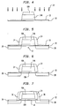
- a gate oxide layer 10 which has been grown on a silicon substrate 12, supports tungsten layers 14 and 16, which comprise the gate electrode of a finished MOS transistor.
- CVD chemical vapor deposition
- evaporation evaporation
- sputtering tungsten films
- CVD tungsten films have high purity and low resistivity; however they are large grained films and do not adhere well to silicon oxide.
- Evaporated tungsten films have a fine grain structure; however they have high electrical resistance and high stress and exhibit poor adhesion to silicon oxide.
- Sputtered tungsten films have a fine grain structure, low electrical resistivity and an adjustable stress level for good silicon oxide adhesion. See C.Y. Ting et al., cited above.
- Tungsten layer 16 is deposited on gate oxide layer 10 a suitable sputter deposition method.
- Sputter deposition methods are well known in the art and are generally performed in a high vacuum deposition system.
- a tungsten target material is bombarded by ions.
- Tungsten atoms are released from the tungsten target and deposit to form a thin tungsten film over the gate oxide layer 10.
- the sputtered tungsten layer 16 is approximately 80nm thick.
- a second tungsten layer 14 is deposited by CVD techniques on top of the sputtered tungsten layer 16.
- CVD techniques are well known in the art and entail passing a vapor containing tungsten atoms over the silicon substrate 12 in a suitable CVD apparatus such that a tungsten film is formed.
- the CVD tungsten layer 14 is approximately 350 nm thick.
- a nitride mask 18 is deposited over the CVD tungsten layer 14 using plasma enhanced chemical vapor deposition or photo enhancement (PECVD) techniques.
- PECVD techniques are also well known in the art. PECVD techniques take advantage of laser or UV light and allow deposition at lower temperatures.
- a resist mask 20 is applied over the nitride mask 18 and is patterned to define a gate electrode.
- the nitride layer 18 is etched in a CF4 plasma etch to form a nitride mask 18A. At this point the resist is stripped.
- the nitride mask 18A now defines placement and pattern the gate electrode.
- a Cl2/O2 plasma etch process is used to etch the CVD tungsten layer 14 which are not protected by the nitrite mask 18A.
- the Cl2/O2 etch takes place in a single plasma etch reactor which typically consists of pressurized chamber, a vacuum supply, an rf power supply connected to an electrode and a grounded electrode.
- the chamber pressure is 13,33 Pa
- the oxygen flow rate is 12 sccm
- the chlorine flow rate is 40 sccm
- the rf power is 625 Watts
- the electrode spacing is kept at 8 cm.
- the etch rate of CVD tungsten is approximately 500 nm/min and the etch rate of sputtered tungsten is significantly less at only 170 nm/min. This shows about a 3:1 difference between CVD tungsten and sputtered tungsten films.
- the sputtered tungsten shows greater resistivity to the Cl2/O2 reactive ion etch processes than does the CVD tungsten.
- the sputtered tungsten acts as a shield for the underlying oxide layer to protect it from ion damage throughout the fabrication process. With this process, the etch ratio of CVD tungsten to mask nitride is more than 10:1.
- Figure 3 shows a top portion of tungsten gate electrode 14A after the Cl2/O2 plasm etch.
- An over-etch of about 30% into the sputtered tungsten layer 16 is needed to compensate for tungsten film non-uniformity and surface topography to ensure that all CVD tungsten not protected by the nitrite mask 18A is removed.
- the gate oxide layer 10 is completely covered and protected by the sputtered tungsten layer 16 throughout the etching process. It is estimated that the thickness of the remaining sputtered tungsten 16 is about 50 ⁇ 5 nm, which is thick enough to effectively shield the oxide layer 10 from reactive ion damage.
- Figure 4 shows the source/drain implant which is performed directly into the remaining sputtered tungsten layer 16.
- Dopant ions 22 are implanted into the sputtered tungsten 16.
- the power of the of the ion implant is regulated such that dopant ions do not penetrate and reach active areas of the gate oxide layer 10 wherein they would cause harm.
- Figure 5 shows a sidewall spacer 24 formed around the CVD tungsten gate electrode 14A and extending laterally over a portion of the sputtered tungsten layer 16.
- the sidewall spacer 24 is made by directional etch back of a suitable CVD dielectric film, such as oxide, nitride, or CVD TEOS (tetraethyl orthosilicate), to leave the film on the sidewalls of the gate electrode.
- a suitable CVD dielectric film such as oxide, nitride, or CVD TEOS (tetraethyl orthosilicate)
- the source 26 and drain 28 regions are formed as the dopants 22 implanted into the sputtered tungsten layer 16 in the source and drain regions diffuse through the gate oxide layer 10 and into the silicon substrate 12.
- portions of the sputtered tungsten layer 16 which are not covered by the sidewall spacer 24 are selectively etched away using a buffered, mildly basic chemical etching solution such as, for example, KH2PO4/KOH/K3Fe(CN)6. This solution will not attack the spacer oxide or the gate oxide material.
- a buffered, mildly basic chemical etching solution such as, for example, KH2PO4/KOH/K3Fe(CN)6.
- KH2PO4/KOH/K3Fe(CN)6 This solution will not attack the spacer oxide or the gate oxide material.
- Such solutions suitable for the practice of the present invention are known in the art and are discussed in T.S. Shakoff et al., High Resolution Tungsten Patterning Using Buffered, Mildly Basic Etching Solutions, J. Electrochem. Soc., Vol. 122, February, 1975, which is herein incorporated by reference.
- Figure 7 shows the finished MOS transistor.
- the gate oxide layer 10 in the source 26 and drain 28 areas is removed using a hydrofluoric acid (BHF) solution.
- a CVD oxide is deposited and etched back to form a second sidewall spacer 30 on the gate electrode sidewalls. This is preferably done in a multi-chamber cluster dep/etch tool.
- the second spacer is used to prevent the gate from shorting with the source 26 and drain 28.
- Silicide, 34 and 32 is formed on top of the exposed source 26 and drain 28 on the silicon surface 12.
- An additional dopant implantation step and subsequent drive-in step may be preformed directly into the silicide 32 and 34 in order to reduce contact and series resistance,.
- refractory metals other than tungsten, may be used in the practice of the present invention.
- Molybdenum is an example of such a refractory metal.
Landscapes
- Insulated Gate Type Field-Effect Transistor (AREA)
- Electrodes Of Semiconductors (AREA)
Applications Claiming Priority (2)
| Application Number | Priority Date | Filing Date | Title |
|---|---|---|---|
| US90086992A | 1992-06-18 | 1992-06-18 | |
| US900869 | 1992-06-18 |
Publications (2)
| Publication Number | Publication Date |
|---|---|
| EP0575280A2 true EP0575280A2 (fr) | 1993-12-22 |
| EP0575280A3 EP0575280A3 (en) | 1995-10-04 |
Family
ID=25413217
Family Applications (1)
| Application Number | Title | Priority Date | Filing Date |
|---|---|---|---|
| EP93480057A Withdrawn EP0575280A3 (en) | 1992-06-18 | 1993-05-05 | Cmos transistor with two-layer inverse-t tungsten gate structure |
Country Status (3)
| Country | Link |
|---|---|
| US (2) | US5599725A (fr) |
| EP (1) | EP0575280A3 (fr) |
| JP (1) | JPH07105498B2 (fr) |
Cited By (1)
| Publication number | Priority date | Publication date | Assignee | Title |
|---|---|---|---|---|
| CN107123677A (zh) * | 2016-02-25 | 2017-09-01 | 台湾积体电路制造股份有限公司 | 鳍片型场效应晶体管装置 |
Families Citing this family (63)
| Publication number | Priority date | Publication date | Assignee | Title |
|---|---|---|---|---|
| US5872733A (en) * | 1995-06-06 | 1999-02-16 | International Business Machines Corporation | Ramp-up rate control circuit for flash memory charge pump |
| KR100190757B1 (ko) * | 1995-06-30 | 1999-06-01 | 김영환 | 모스 전계 효과 트랜지스터 형성방법 |
| JP3714995B2 (ja) * | 1995-07-05 | 2005-11-09 | シャープ株式会社 | 半導体装置 |
| US5597746A (en) * | 1995-08-09 | 1997-01-28 | Micron Technology, Inc. | Method of forming field effect transistors relative to a semiconductor substrate and field effect transistors produced according to the method |
| JPH09232568A (ja) * | 1996-02-14 | 1997-09-05 | Taiwan Moseki Denshi Kofun Yugenkoshi | 逆t字型ゲートmosトランジスタをもつldd及びその製造方法 |
| US5808362A (en) * | 1996-02-29 | 1998-09-15 | Motorola, Inc. | Interconnect structure and method of forming |
| US5858867A (en) * | 1996-05-20 | 1999-01-12 | Mosel Vitelic, Inc. | Method of making an inverse-T tungsten gate |
| US6159815A (en) * | 1996-09-27 | 2000-12-12 | Siemens Aktiengesellschaft | Method of producing a MOS transistor |
| US6160277A (en) * | 1996-10-28 | 2000-12-12 | Micron Technology, Inc. | Field effect transistor assemblies and transistor gate block stacks |
| JP2882395B2 (ja) * | 1997-03-24 | 1999-04-12 | 日本電気株式会社 | 半導体集積回路装置及びその製造方法 |
| US6133608A (en) * | 1997-04-23 | 2000-10-17 | International Business Machines Corporation | SOI-body selective link method and apparatus |
| US6160292A (en) * | 1997-04-23 | 2000-12-12 | International Business Machines Corporation | Circuit and methods to improve the operation of SOI devices |
| US6440750B1 (en) | 1997-06-10 | 2002-08-27 | Agere Systems Guardian Corporation | Method of making integrated circuit having a micromagnetic device |
| US6118351A (en) * | 1997-06-10 | 2000-09-12 | Lucent Technologies Inc. | Micromagnetic device for power processing applications and method of manufacture therefor |
| US5783479A (en) * | 1997-06-23 | 1998-07-21 | National Science Council | Structure and method for manufacturing improved FETs having T-shaped gates |
| US6025635A (en) * | 1997-07-09 | 2000-02-15 | Advanced Micro Devices, Inc. | Short channel transistor having resistive gate extensions |
| JP3702611B2 (ja) * | 1997-10-06 | 2005-10-05 | ソニー株式会社 | 固体撮像素子及びその製造方法 |
| US5837588A (en) * | 1998-01-26 | 1998-11-17 | Texas Instruments-Acer Incorporated | Method for forming a semiconductor device with an inverse-T gate lightly-doped drain structure |
| US6369709B1 (en) * | 1998-04-10 | 2002-04-09 | 3M Innovative Properties Company | Terminal for libraries and the like |
| US5869374A (en) * | 1998-04-22 | 1999-02-09 | Texas Instruments-Acer Incorporated | Method to form mosfet with an inverse T-shaped air-gap gate structure |
| US6410369B1 (en) | 1998-04-22 | 2002-06-25 | International Business Machines Corporation | Soi-body selective link method and apparatus |
| US6097056A (en) * | 1998-04-28 | 2000-08-01 | International Business Machines Corporation | Field effect transistor having a floating gate |
| US6049114A (en) * | 1998-07-20 | 2000-04-11 | Motorola, Inc. | Semiconductor device having a metal containing layer overlying a gate dielectric |
| KR100275739B1 (ko) * | 1998-08-14 | 2000-12-15 | 윤종용 | 역방향 자기정합 구조의 트랜지스터 및 그 제조방법 |
| US6110788A (en) * | 1998-09-16 | 2000-08-29 | Micron Technology, Inc. | Surface channel MOS transistors, methods for making the same, and semiconductor devices containing the same |
| US6909114B1 (en) | 1998-11-17 | 2005-06-21 | Semiconductor Energy Laboratory Co., Ltd. | Semiconductor device having LDD regions |
| KR100291513B1 (ko) | 1998-12-22 | 2001-07-12 | 박종섭 | 반도체 소자의 제조방법 |
| KR100296126B1 (ko) | 1998-12-22 | 2001-08-07 | 박종섭 | 고집적 메모리 소자의 게이트전극 형성방법 |
| KR100324024B1 (ko) | 1998-12-28 | 2002-05-13 | 박종섭 | 반도체소자의게이트전극형성방법 |
| KR100299386B1 (ko) | 1998-12-28 | 2001-11-02 | 박종섭 | 반도체 소자의 게이트 전극 형성방법 |
| KR100345364B1 (ko) | 1998-12-28 | 2002-09-18 | 주식회사 하이닉스반도체 | 반도체 소자의 게이트전극 형성방법 |
| JP3988342B2 (ja) | 1998-12-29 | 2007-10-10 | 株式会社ハイニックスセミコンダクター | 半導体素子のゲート電極形成方法 |
| US6448140B1 (en) | 1999-02-08 | 2002-09-10 | Taiwan Semiconductor Manufacturing Company | Laterally recessed tungsten silicide gate structure used with a self-aligned contact structure including a straight walled sidewall spacer while filling recess |
| US6521501B1 (en) * | 1999-05-11 | 2003-02-18 | Advanced Micro Devices, Inc. | Method of forming a CMOS transistor having ultra shallow source and drain regions |
| US6255714B1 (en) | 1999-06-22 | 2001-07-03 | Agere Systems Guardian Corporation | Integrated circuit having a micromagnetic device including a ferromagnetic core and method of manufacture therefor |
| KR100295062B1 (ko) * | 1999-08-17 | 2001-07-12 | 윤종용 | 게이트 산화막의 손상을 회복시키는 반도체장치의 게이트 제조방법 |
| US6183035B1 (en) * | 1999-09-02 | 2001-02-06 | The Budd Company | Tonneau cover and attachment assembly |
| US6338520B2 (en) | 1999-09-02 | 2002-01-15 | The Budd Company | Tonneau cover and attachment assembly |
| US6423644B1 (en) * | 2000-07-12 | 2002-07-23 | Applied Materials, Inc. | Method of etching tungsten or tungsten nitride electrode gates in semiconductor structures |
| US6440870B1 (en) | 2000-07-12 | 2002-08-27 | Applied Materials, Inc. | Method of etching tungsten or tungsten nitride electrode gates in semiconductor structures |
| KR100363710B1 (ko) * | 2000-08-23 | 2002-12-05 | 삼성전자 주식회사 | 셀프-얼라인 콘택 구조를 갖는 반도체 장치 및 그 제조방법 |
| DE10142340B4 (de) * | 2001-08-30 | 2006-04-13 | Infineon Technologies Ag | Feldeffekttransistor mit einem Kontakt zu einem seiner Dotiergebiete und Verfahren zu seiner Herstellung |
| US6509221B1 (en) | 2001-11-15 | 2003-01-21 | International Business Machines Corporation | Method for forming high performance CMOS devices with elevated sidewall spacers |
| DE10163557B4 (de) * | 2001-12-21 | 2007-12-06 | Forschungszentrum Jülich GmbH | Transistorbasierter Sensor mit besonders ausgestalteter Gateelektrode zur hochempfindlichen Detektion von Analyten |
| US20030235995A1 (en) * | 2002-06-21 | 2003-12-25 | Oluseyi Hakeem M. | Method of increasing selectivity to mask when etching tungsten or tungsten nitride |
| JP2004071959A (ja) * | 2002-08-08 | 2004-03-04 | Renesas Technology Corp | 半導体装置 |
| US6936508B2 (en) * | 2003-09-12 | 2005-08-30 | Texas Instruments Incorporated | Metal gate MOS transistors and methods for making the same |
| US7148546B2 (en) | 2003-09-30 | 2006-12-12 | Texas Instruments Incorporated | MOS transistor gates with doped silicide and methods for making the same |
| US7015534B2 (en) * | 2003-10-14 | 2006-03-21 | Texas Instruments Incorporated | Encapsulated MOS transistor gate structures and methods for making the same |
| JP4828790B2 (ja) * | 2003-10-22 | 2011-11-30 | 独立行政法人産業技術総合研究所 | Mosfet型半導体装置の製造方法 |
| US7045456B2 (en) * | 2003-12-22 | 2006-05-16 | Texas Instruments Incorporated | MOS transistor gates with thin lower metal silicide and methods for making the same |
| US6974736B2 (en) * | 2004-01-09 | 2005-12-13 | International Business Machines Corporation | Method of forming FET silicide gate structures incorporating inner spacers |
| US7491644B2 (en) * | 2004-09-10 | 2009-02-17 | Commissariat A L'energie Atomique | Manufacturing process for a transistor made of thin layers |
| FR2875334B1 (fr) * | 2004-09-10 | 2007-02-23 | Commissariat Energie Atomique | Procede de fabrication d'un transistor realise en couches minces |
| US20090275182A1 (en) * | 2008-05-01 | 2009-11-05 | International Business Machines Corporation | Method for fabricating a metal high dielectric constant transistor with reverse-t gate |
| US7736981B2 (en) * | 2008-05-01 | 2010-06-15 | International Business Machines Corporation | Metal high dielectric constant transistor with reverse-T gate |
| US20100155860A1 (en) * | 2008-12-24 | 2010-06-24 | Texas Instruments Incorporated | Two step method to create a gate electrode using a physical vapor deposited layer and a chemical vapor deposited layer |
| JP5210915B2 (ja) | 2009-02-09 | 2013-06-12 | 株式会社東芝 | 半導体装置の製造方法 |
| SG165252A1 (en) | 2009-03-25 | 2010-10-28 | Unisantis Electronics Jp Ltd | Semiconductor device and production method therefor |
| JP5032532B2 (ja) * | 2009-06-05 | 2012-09-26 | ユニサンティス エレクトロニクス シンガポール プライベート リミテッド | 半導体装置及びその製造方法 |
| JP5006378B2 (ja) | 2009-08-11 | 2012-08-22 | ユニサンティス エレクトロニクス シンガポール プライベート リミテッド | 半導体装置及びその製造方法 |
| JP5006379B2 (ja) * | 2009-09-16 | 2012-08-22 | ユニサンティス エレクトロニクス シンガポール プライベート リミテッド | 半導体装置 |
| US9412859B2 (en) * | 2013-03-11 | 2016-08-09 | Globalfoundries Inc. | Contact geometry having a gate silicon length decoupled from a transistor length |
Family Cites Families (21)
| Publication number | Priority date | Publication date | Assignee | Title |
|---|---|---|---|---|
| US4319932A (en) * | 1980-03-24 | 1982-03-16 | International Business Machines Corporation | Method of making high performance bipolar transistor with polysilicon base contacts |
| US4356623A (en) * | 1980-09-15 | 1982-11-02 | Texas Instruments Incorporated | Fabrication of submicron semiconductor devices |
| US4901128A (en) * | 1982-11-04 | 1990-02-13 | Hitachi, Ltd. | Semiconductor memory |
| JPS59162276A (ja) * | 1983-03-07 | 1984-09-13 | Toshiba Corp | 反応性イオンエツチング方法 |
| US4672419A (en) * | 1984-06-25 | 1987-06-09 | Texas Instruments Incorporated | Metal gate, interconnect and contact system for VLSI devices |
| JPS6273779A (ja) * | 1985-09-27 | 1987-04-04 | Oki Electric Ind Co Ltd | 半導体素子の製造方法 |
| JPS6342173A (ja) * | 1986-08-07 | 1988-02-23 | Fujitsu Ltd | 絶縁ゲ−ト型半導体装置の製造方法 |
| US4786360A (en) * | 1987-03-30 | 1988-11-22 | International Business Machines Corporation | Anisotropic etch process for tungsten metallurgy |
| KR970003903B1 (en) * | 1987-04-24 | 1997-03-22 | Hitachi Mfg Kk | Semiconductor device and fabricating method thereof |
| US4963504A (en) * | 1987-11-23 | 1990-10-16 | Xerox Corporation | Method for fabricating double implanted LDD transistor self-aligned with gate |
| JPH01206667A (ja) * | 1988-02-15 | 1989-08-18 | Toshiba Corp | Mos型集積回路およびその製造方法 |
| JPH0724261B2 (ja) * | 1989-01-20 | 1995-03-15 | 株式会社東芝 | 半導体装置の製造方法 |
| US4906589A (en) * | 1989-02-06 | 1990-03-06 | Industrial Technology Research Institute | Inverse-T LDDFET with self-aligned silicide |
| US4984042A (en) * | 1989-02-13 | 1991-01-08 | Motorola, Inc. | MOS transistors using selective polysilicon deposition |
| US5217923A (en) * | 1989-02-13 | 1993-06-08 | Kabushiki Kaisha Toshiba | Method of fabricating a semiconductor device having silicided source/drain regions |
| JPH03248568A (ja) * | 1990-02-27 | 1991-11-06 | Fuji Xerox Co Ltd | 薄膜半導体装置 |
| US5306655A (en) * | 1990-07-24 | 1994-04-26 | Matsushita Electric Industrial Co., Ltd. | Structure and method of manufacture for MOS field effect transistor having lightly doped drain and source diffusion regions |
| US5097301A (en) * | 1990-12-19 | 1992-03-17 | Intel Corporation | Composite inverse T-gate metal oxide semiconductor device and method of fabrication |
| US5162884A (en) * | 1991-03-27 | 1992-11-10 | Sgs-Thomson Microelectronics, Inc. | Insulated gate field-effect transistor with gate-drain overlap and method of making the same |
| US5182619A (en) * | 1991-09-03 | 1993-01-26 | Motorola, Inc. | Semiconductor device having an MOS transistor with overlapped and elevated source and drain |
| US5282972A (en) * | 1991-12-18 | 1994-02-01 | Kelco Water Engineering, Inc. | Method and apparatus for recycling R/O waste water |
-
1993
- 1993-05-05 EP EP93480057A patent/EP0575280A3/en not_active Withdrawn
- 1993-06-01 JP JP5130517A patent/JPH07105498B2/ja not_active Expired - Fee Related
-
1994
- 1994-11-22 US US08/346,210 patent/US5599725A/en not_active Expired - Fee Related
-
1996
- 1996-05-15 US US08/648,457 patent/US5633522A/en not_active Expired - Fee Related
Cited By (1)
| Publication number | Priority date | Publication date | Assignee | Title |
|---|---|---|---|---|
| CN107123677A (zh) * | 2016-02-25 | 2017-09-01 | 台湾积体电路制造股份有限公司 | 鳍片型场效应晶体管装置 |
Also Published As
| Publication number | Publication date |
|---|---|
| US5599725A (en) | 1997-02-04 |
| US5633522A (en) | 1997-05-27 |
| JPH07105498B2 (ja) | 1995-11-13 |
| JPH0653495A (ja) | 1994-02-25 |
| EP0575280A3 (en) | 1995-10-04 |
Similar Documents
| Publication | Publication Date | Title |
|---|---|---|
| US5599725A (en) | Method for fabricating a MOS transistor with two-layer inverse-T tungsten gate structure | |
| US5350698A (en) | Multilayer polysilicon gate self-align process for VLSI CMOS device | |
| US5650342A (en) | Method of making a field effect transistor with a T shaped polysilicon gate electrode | |
| EP0315229B1 (fr) | Procédé pour la fabrication d'un dispositif à semi-conducteur à structure de la grille isolée | |
| US5773348A (en) | Method of fabricating a short-channel MOS device | |
| US4855247A (en) | Process for fabricating self-aligned silicide lightly doped drain MOS devices | |
| US6475888B1 (en) | Method for forming ultra-shallow junctions using laser annealing | |
| US4149904A (en) | Method for forming ion-implanted self-aligned gate structure by controlled ion scattering | |
| US5200351A (en) | Method of fabricating field effect transistors having lightly doped drain regions | |
| US5175119A (en) | Method of producing insulated-gate field effect transistor | |
| US5858867A (en) | Method of making an inverse-T tungsten gate | |
| US4744859A (en) | Process for fabricating lightly doped drain MOS devices | |
| US6949436B2 (en) | Composite spacer liner for improved transistor performance | |
| US20030003750A1 (en) | Disposable spacer and method of forming and using same | |
| US5972761A (en) | Method of making MOS transistors with a gate-side air-gap structure and an extension ultra-shallow S/D junction | |
| US6200840B1 (en) | Method for producing PMOS devices | |
| GB2322005A (en) | Semiconductor device and manufacturing method of the same | |
| US6649308B1 (en) | Ultra-short channel NMOSFETS with self-aligned silicide contact | |
| JPH0475351A (ja) | 化合物半導体装置の製造方法 | |
| US6221745B1 (en) | High selectivity mask oxide etching to suppress silicon pits | |
| JPH0147016B2 (fr) | ||
| EP0942467B1 (fr) | Procédé de fabrication des dispositifs bipolaires et BiCMOS | |
| US5963839A (en) | Reduction of polysilicon contact resistance by nitrogen implantation | |
| KR100439770B1 (ko) | 반도체 장치의 제조방법 | |
| US6365471B1 (en) | Method for producing PMOS devices |
Legal Events
| Date | Code | Title | Description |
|---|---|---|---|
| PUAI | Public reference made under article 153(3) epc to a published international application that has entered the european phase |
Free format text: ORIGINAL CODE: 0009012 |
|
| AK | Designated contracting states |
Kind code of ref document: A2 Designated state(s): DE FR GB |
|
| 17P | Request for examination filed |
Effective date: 19940429 |
|
| PUAL | Search report despatched |
Free format text: ORIGINAL CODE: 0009013 |
|
| AK | Designated contracting states |
Kind code of ref document: A3 Designated state(s): DE FR GB |
|
| STAA | Information on the status of an ep patent application or granted ep patent |
Free format text: STATUS: THE APPLICATION HAS BEEN WITHDRAWN |
|
| 18W | Application withdrawn |
Withdrawal date: 19960412 |