EP0576770A1 - Circuit de commande pour débrancher un amplificateur audio - Google Patents
Circuit de commande pour débrancher un amplificateur audio Download PDFInfo
- Publication number
- EP0576770A1 EP0576770A1 EP92830253A EP92830253A EP0576770A1 EP 0576770 A1 EP0576770 A1 EP 0576770A1 EP 92830253 A EP92830253 A EP 92830253A EP 92830253 A EP92830253 A EP 92830253A EP 0576770 A1 EP0576770 A1 EP 0576770A1
- Authority
- EP
- European Patent Office
- Prior art keywords
- output
- voltage
- circuit
- terminal
- transistor
- Prior art date
- Legal status (The legal status is an assumption and is not a legal conclusion. Google has not performed a legal analysis and makes no representation as to the accuracy of the status listed.)
- Granted
Links
Images

Classifications
-
- H—ELECTRICITY
- H03—ELECTRONIC CIRCUITRY
- H03F—AMPLIFIERS
- H03F1/00—Details of amplifiers with only discharge tubes, only semiconductor devices or only unspecified devices as amplifying elements
- H03F1/30—Modifications of amplifiers to reduce influence of variations of temperature or supply voltage or other physical parameters
- H03F1/305—Modifications of amplifiers to reduce influence of variations of temperature or supply voltage or other physical parameters in case of switching on or off of a power supply
-
- H—ELECTRICITY
- H03—ELECTRONIC CIRCUITRY
- H03G—CONTROL OF AMPLIFICATION
- H03G3/00—Gain control in amplifiers or frequency changers
- H03G3/20—Automatic control
- H03G3/30—Automatic control in amplifiers having semiconductor devices
- H03G3/34—Muting amplifier when no signal is present
- H03G3/348—Muting in response to a mechanical action or to power supply variations, e.g. during tuning; Click removal circuits
Definitions
- the present invention relates to a circuit for turn-off control of audio amplifiers, in particular, single-ended, single-feed types.
- All audio amplifiers present a noise filtering capacitor between the supply line and ground. Due to the widely varying frequency and peak value of the noise at the supply, the filter capacitor presents a fairly high value, whereas the equivalent resistance of the overall amplifier circuit is small, thus resulting in a small discharge constant and in fairly fast discharge of the capacitor itself.
- an audio amplifier turn-off control circuit as claimed in Claim 1.
- the present invention thus provides for a circuit which, when the power supply is cut off, locks the output to the supply line, the potential of which is gradually reduced by virtue of the filter capacitor, so that the output follows the supply line, with the same slope, and is thus controlled by the filter capacitor.
- the audio amplifier indicated as a whole by 1, is represented by the cascade connection of two stages, more specifically, an input stage 2 having a high transconductance g m , and a gain stage 3 with gain -A v .
- the positive input IN+ of input stage 2 is supplied in known manner with the audio signal, while the negative input IN- is connected to output 9 of amplifier 1 via a feedback network 4 including a pair of resistors 5, 6 connected between the output and ground, and a capacitor 7 connected between the mid point of resistors 5, 6 and negative input IN-.
- a compensating capacitor 8 is provided between the input and output of gain stage 3.
- a PNP type transistor 10 is provided for locking output 9 of amplifier 1 and supply line 11. More specifically, transistor 10 presents the collector connected to the input of gain stage 3, the emitter connected to output 9 via the interposition of a high-value resistor 12, and the base connected to the output of a control block 13 for generating a potential V B in relation to ground.
- the emitter of transistor 10, at which potential V D is present, is also groundable by a switch 15 having a control terminal 16 also controlled by control block 13.
- Control block 13 is in turn connected to supply line 11, set to potential V S in relation to ground, and to a voltage source 17 for generating a lower potential V A in relation to ground as compared with steady-state supply voltage V CC .
- source 17 comprises a capacitor 18 and a resistor 19 parallel-connected between node 20 and ground, node 20 being connected to supply line 11 via a branch 22 formed by the series connection of at least one diode 23 and a resistor 24 (but possibly comprising a number of diodes and resistors).
- the Fig.1 circuit is completed by a filter capacitor 25 for filtering noise on supply line 11 and located between line 11 and ground; a resistor 26 representing the equivalent resistance of amplifier 1 as seen by filter capacitor 25 and in which capacitor 25 discharges when the power supply is cut off; and a switch 27 between supply line 11 and input 28 at which the voltage V CC supplied by an external power supply unit (not shown) is present.
- the time constant of the filter formed by components 25, 26 is smaller than that of filter 17 formed by components 18, 19, so that capacitor 25 discharges faster than capacitor 18, the voltage of which may thus be assumed more or less constant as regards the circuit according to the present invention.
- transistor 10 When activated, transistor 10, by which the output of audio amplifier 1 is locked to supply line 11, thus provides for local feedback between the amplifier output and the input of the gain stage.
- the transistor 10 and gain stage 3 structure may be represented schematically by an equivalent operational amplifier having a positive input corresponding to the base terminal of transistor 10, a negative input corresponding to the emitter of transistor 10 (with switch 15 open), and an output corresponding to output 9 of amplifier 1; and which, despite being closed in unit-gain manner by resistor 12, is stable.
- the stability of the equivalent operational amplifier is explainable by comparing it with audio amplifier 1. Both present gain stage 3 with compensating capacitor 8, but, whereas input stage 2 of amplifier 1 presents a high transconductance, the transconductance of the equivalent operational amplifier equals the inverse of the resistance of resistor 12 (1/R g , where R g is the resistance of resistor 12) which, by appropriately selecting R g , is much lower than g m . As a result, the loop gain of the operational amplifier is sufficiently lower as compared with audio amplifier 1 to achieve a lower closed-loop gain for a given degree of stability.
- the turn-off phase commences when switch 27 is opened (instant t O ), at which point, capacitor 25 discharges rapidly into resistor 26, thus causing a corresponding reduction in V S ; and, at the same time, voltage V A at point 20 is reduced by virtue of capacitor 18 discharging into resistor 19, but at a slower rate than capacitor 25.
- control block 13 Upon V S falling below V A (instant t1), control block 13 switches and emits a signal for opening switch 15; switch 15 opens so that the emitter of transistor 10 is no longer grounded; and the emitter substantially switches to potential V o of output 9 of audio amplifier 1.
- Control block 13 also modifies the value of potential V B so that it follows voltage V S over supply line 11. Potential V B thus begins to fall, but, as V B > V D - V BE (where V BE is the base-emitter voltage drop of transistor 10, and, at this phase, V D ⁇ V o ) still applies, transistor 10 remains off.
- transistor 10 Upon V B falling below V D - V BE (instant t2), transistor 10 comes on and locks output 9 to voltage V B at its base and, consequently, to supply voltage V S , so that output 9 is grounded in controlled manner by the discharging of capacitor 25.
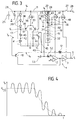
- Fig.3 shows a circuit embodiment, by way of example, of the Fig.1 blocks, in which can be seen stages 2 and 3 of audio amplifier 1; capacitors 25 and 18; resistors 12 and 26; supply line 11; switch 27; transistor 10; and branch 22 including diode 23 and resistor 24.
- resistor 19 is formed by the series connection of a resistor 30 (connected to capacitor 18 at node 46) and two pairs of diodes 31, 32; and block 13 comprises a differential stage 33 formed by two PNP type transistors 34, 35 having the emitters connected to each other and to a current source 36 also connected to supply line 11.
- the base of transistor 35 is connected to node 43 between resistor 24 and the anode of diode 23 (set to potential V E ), while the base of transistor 34 is connected to node 37 of a branch 38 formed by three diodes 39 series-connected between supply line 11 and node 37 (with the cathode facing node 37), and by two series-connected resistors 40, 41 between node 37 and ground.
- Node 42 between resistors 40, 41 is connected to the base of transistor 10; the collector of transistor 34 is grounded; the collector of transistor 35 is connected to the anode of a diode 44 having its cathode grounded and which, together with an NPN type transistor 45, forms switch 15; and transistor 45 presents its base connected to the anode of diode 44, its emitter grounded, and its collector connected to the emitter of transistor 10 at node 49.
- Fig.3 also shows, schematically, current sources 47 and 48 respectively relative to input stage 2 and gain stage 3, and controlled by the potential at node 50 between resistor 30 and the series connection of diodes 31, 32.
- Feedback network 4 and compensating capacitor 8 (connected as in Fig.1) are not shown in the Fig.3 circuit, which shows the connection, via resistor 52, of positive input IN+ of input stage 2 to a node 51 between diodes 31 and 32.
- Input IN+ of input stage 2 is supplied with the audio signal via a decoupling capacitor 53.
- the Fig.3 circuit operates as follows.
- transistor 35 When this applies, transistor 35 is turned off, transistor 34 turned on, and consequently diode 44 and transistor 45 turned off. As the base-emitter voltage drop of transistor 10 prevents it from being turned on, potential V D follows output voltage V o of audio amplifier 1, so that the output voltage remains constant. 3) V C ⁇ V E and V B ⁇ V D - V BE
- transistor 10 comes on so as to ground output 9 (locked to the emitter of transistor 10) according to the fall in potential V B at the base of the transistor and consequently also in V S .
- circuit according to the present invention provides for ensuring controlled reduction at all times of the output during turn-off, and so preventing undesired noise (popping) caused by transients occurring in the system.
- the first phase in the operation of the control circuit prevents the circuit from operating under steady-state conditions, in the event of temporary failure or a negligible fall in supply; while the second phase enables the emitter of transistor 10 to reach the output voltage value before voltage V B falls below the steady-state output voltage value minus V BE , thus preventing an undesired step transient and, consequently, popping of the amplifier output when switch 15 is opened.
- V C > V E which undoubtedly applies by virtue of both V C and V E presenting a fixed direct current offset and being unaffected by the signal
- V B > (V D ) DC + (V D ) AC - V BE where (V D ) DC and (V D ) AC are respectively the direct and alternating current offset of the potential at node 49, so that transistor 10 definitely remains off.
- the circuit When supply is cut off in the presence of a signal, the circuit operates in the same way as described above, except that the value of V D varies, so that transistor 10 alternates between phases wherein supply is locked and phases of inactivity, depending on the amplitude and frequency of the signal, the mean value of output 9, however, being grounded as shown in Fig.4.
- the circuit according to the present invention is straightforward in design, reliable, and provides for troublefree manufacture and integration using current techniques. Moreover, the control circuit employs characteristics of the amplifier that are useful for other and/or existing functions, i.e. timing by the capacitors necessarily provided for in the application, and the references of the chain formed by branches 22, 19, which may also be employed for normal operation of the audio amplifier.
- voltage source 17 in Fig.1 may be implemented differently, either as a unit designed to maintain a constant voltage at its terminals, or a unit whose voltage falls alongside a fall in supply, providing the unit voltage falls more slowly than supply.
- control feedback loop is located between the input and output of the gain stage only, is preferable in terms of stability, other solutions also including the input stage in the control loop are possible by connecting the feedback element (transistor 10) between the output and input of audio amplifier 1 as a whole.
Landscapes
- Engineering & Computer Science (AREA)
- Power Engineering (AREA)
- Amplifiers (AREA)
Priority Applications (5)
| Application Number | Priority Date | Filing Date | Title |
|---|---|---|---|
| EP92830253A EP0576770B1 (fr) | 1992-05-22 | 1992-05-22 | Circuit de commande pour débrancher un amplificateur audio |
| DE1992630466 DE69230466T2 (de) | 1992-05-22 | 1992-05-22 | Abschaltsteuerschaltung für einen Audioverstärker |
| US08/065,672 US5420535A (en) | 1992-05-22 | 1993-05-21 | Audio amplifier turn-off control circuit |
| JP5120033A JPH0637548A (ja) | 1992-05-22 | 1993-05-21 | ターンオフ制御回路 |
| US08/337,108 US5703528A (en) | 1992-05-22 | 1994-11-10 | Audio amplifier turn-off control circuit |
Applications Claiming Priority (2)
| Application Number | Priority Date | Filing Date | Title |
|---|---|---|---|
| EP92830253A EP0576770B1 (fr) | 1992-05-22 | 1992-05-22 | Circuit de commande pour débrancher un amplificateur audio |
| US08/337,108 US5703528A (en) | 1992-05-22 | 1994-11-10 | Audio amplifier turn-off control circuit |
Publications (2)
| Publication Number | Publication Date |
|---|---|
| EP0576770A1 true EP0576770A1 (fr) | 1994-01-05 |
| EP0576770B1 EP0576770B1 (fr) | 1999-12-22 |
Family
ID=26132557
Family Applications (1)
| Application Number | Title | Priority Date | Filing Date |
|---|---|---|---|
| EP92830253A Expired - Lifetime EP0576770B1 (fr) | 1992-05-22 | 1992-05-22 | Circuit de commande pour débrancher un amplificateur audio |
Country Status (3)
| Country | Link |
|---|---|
| US (2) | US5420535A (fr) |
| EP (1) | EP0576770B1 (fr) |
| JP (1) | JPH0637548A (fr) |
Cited By (1)
| Publication number | Priority date | Publication date | Assignee | Title |
|---|---|---|---|---|
| EP1122882A3 (fr) * | 1999-12-27 | 2004-09-22 | Semiconductor Technology Academic Research Center | Circuit amplificateur |
Families Citing this family (25)
| Publication number | Priority date | Publication date | Assignee | Title |
|---|---|---|---|---|
| EP0576770B1 (fr) * | 1992-05-22 | 1999-12-22 | STMicroelectronics S.r.l. | Circuit de commande pour débrancher un amplificateur audio |
| US5939938A (en) * | 1995-10-13 | 1999-08-17 | National Semiconductor Corporation | Amplifier circuit with reduced DC power related turn-on and turn-off transients |
| JP3537571B2 (ja) * | 1995-12-05 | 2004-06-14 | ローム株式会社 | オーディオ信号増幅回路 |
| US5796303A (en) * | 1996-06-26 | 1998-08-18 | Vinn; Charles L. | Popless amplifier |
| GB2322746A (en) * | 1997-02-26 | 1998-09-02 | Thomson Multimedia Sa | Preventing pop noise in TV sound |
| US6040740A (en) * | 1997-04-09 | 2000-03-21 | Lsi Logic Corporation | Audio transient suppression device |
| US6154548A (en) * | 1997-09-27 | 2000-11-28 | Ati Technologies | Audio mute control signal generating circuit |
| US6249796B1 (en) | 1998-12-08 | 2001-06-19 | Siemens Medical Systems, Inc. | Real-time technique for reducing the settling time of a high pass filter |
| US6621907B1 (en) * | 1999-06-24 | 2003-09-16 | Randall C. Smith | Mute circuit for use with switching relays |
| JP4766732B2 (ja) * | 2000-07-11 | 2011-09-07 | 新日本無線株式会社 | オーディオアンプのバイアス回路 |
| US6346854B1 (en) * | 2000-10-31 | 2002-02-12 | National Semiconductor Corporation | Amplifier circuit with reduced DC power related turn-on and turn-off transients |
| CN1214518C (zh) * | 2001-02-10 | 2005-08-10 | 深圳赛意法微电子有限公司 | 用于音频放大器的关机噪声抑制电路 |
| DE10223996B4 (de) * | 2002-05-29 | 2004-12-02 | Infineon Technologies Ag | Referenzspannungsschaltung und Verfahren zum Erzeugen einer Referenzspannung |
| JP4076373B2 (ja) * | 2002-06-04 | 2008-04-16 | ローム株式会社 | 音声出力装置を有する電子装置 |
| US7187513B2 (en) * | 2002-06-14 | 2007-03-06 | Renesas Technology America, Inc. | Differential magneto-resistive head pre-amplifiers for single polarity power supply applications |
| FR2853472B1 (fr) * | 2003-04-01 | 2005-06-24 | St Microelectronics Sa | Circuit amplificateur audio |
| US7164312B1 (en) * | 2004-08-02 | 2007-01-16 | National Semiconductor Corporation | Apparatus and method for pop-and-click suppression with fast turn-on time |
| TW200640127A (en) * | 2005-05-03 | 2006-11-16 | Elite Semiconductor Esmt | Audio amplifying device capable of preventing pop noise |
| TWI317240B (en) * | 2006-07-05 | 2009-11-11 | Asustek Comp Inc | Anti-pop circuit |
| US7830206B2 (en) * | 2007-08-08 | 2010-11-09 | Sanyo Electric Co., Ltd. | Amplifier circuit |
| JP5144308B2 (ja) * | 2008-02-25 | 2013-02-13 | ラピスセミコンダクタ株式会社 | オペアンプ回路及びオペアンプ回路の駆動方法 |
| JP4759015B2 (ja) * | 2008-04-25 | 2011-08-31 | 株式会社リコー | 定電圧回路 |
| EP2650317A1 (fr) | 2010-12-10 | 2013-10-16 | Mitsubishi Gas Chemical Company, Inc. | Résine polyester et lentille optique |
| US20170044311A1 (en) | 2014-04-24 | 2017-02-16 | Mitsubishi Gas Chemical Company, Inc. | Polyester resin, optical lens, and optical lens system |
| FR3072221B1 (fr) * | 2017-10-09 | 2021-03-26 | Continental Automotive France | Dispositif d’alimentation d’un calculateur electronique |
Citations (4)
| Publication number | Priority date | Publication date | Assignee | Title |
|---|---|---|---|---|
| US3840820A (en) * | 1971-12-17 | 1974-10-08 | Sony Corp | Muting circuit |
| EP0069843A1 (fr) * | 1981-07-10 | 1983-01-19 | Deutsche Thomson-Brandt GmbH | Amplificateur BF pour un récepteur de télévision |
| EP0281117A2 (fr) * | 1987-03-06 | 1988-09-07 | Kabushiki Kaisha Toshiba | Circuit pour la suppression de bruit de commutation dans un amplificateur audio |
| EP0368528A2 (fr) * | 1988-11-09 | 1990-05-16 | STMicroelectronics S.r.l. | Amplificateur audio avec états d'attente et muets |
Family Cites Families (14)
| Publication number | Priority date | Publication date | Assignee | Title |
|---|---|---|---|---|
| JPS5715486B2 (fr) * | 1974-04-30 | 1982-03-31 | ||
| JPS52136526U (fr) * | 1976-04-09 | 1977-10-17 | ||
| JPS5442447U (fr) * | 1977-08-29 | 1979-03-22 | ||
| JPS6038043B2 (ja) * | 1978-09-27 | 1985-08-29 | パイオニア株式会社 | スイツチ回路 |
| DE2931144A1 (de) * | 1979-08-01 | 1981-02-19 | Philips Patentverwaltung | Schaltungsanordnung zum beseitigen des ein- und ausschaltknackens bei einem verstaerker |
| JPS5672510A (en) * | 1979-11-20 | 1981-06-16 | Toshiba Corp | Muting circuit |
| JPS59230306A (ja) * | 1983-06-14 | 1984-12-24 | Matsushita Electric Ind Co Ltd | ミユ−テイング回路 |
| JPS60123111A (ja) * | 1983-12-07 | 1985-07-01 | Hitachi Micro Comput Eng Ltd | 増幅回路 |
| JP2609723B2 (ja) * | 1989-05-31 | 1997-05-14 | 株式会社東芝 | 増幅回路 |
| US5255094A (en) * | 1990-10-10 | 1993-10-19 | Thomson Consumer Electronics, S.A. | Muting circuit for eliminating transient signals generated due to power supply turn-on and turn-off |
| US5199079A (en) * | 1991-05-21 | 1993-03-30 | Thomson Consumer Electronics, Inc. | Supply voltage responsive audible transient (POP) suppression arrangement |
| EP0576770B1 (fr) * | 1992-05-22 | 1999-12-22 | STMicroelectronics S.r.l. | Circuit de commande pour débrancher un amplificateur audio |
| US5307025A (en) * | 1992-07-14 | 1994-04-26 | Media Vision, Inc. | Audio power amplifier with noise prevention at turn-on and turn-off |
| JPH06244644A (ja) * | 1993-02-15 | 1994-09-02 | Pioneer Electron Corp | カーオーディオシステムにおけるミュート装置 |
-
1992
- 1992-05-22 EP EP92830253A patent/EP0576770B1/fr not_active Expired - Lifetime
-
1993
- 1993-05-21 JP JP5120033A patent/JPH0637548A/ja active Pending
- 1993-05-21 US US08/065,672 patent/US5420535A/en not_active Expired - Lifetime
-
1994
- 1994-11-10 US US08/337,108 patent/US5703528A/en not_active Expired - Lifetime
Patent Citations (4)
| Publication number | Priority date | Publication date | Assignee | Title |
|---|---|---|---|---|
| US3840820A (en) * | 1971-12-17 | 1974-10-08 | Sony Corp | Muting circuit |
| EP0069843A1 (fr) * | 1981-07-10 | 1983-01-19 | Deutsche Thomson-Brandt GmbH | Amplificateur BF pour un récepteur de télévision |
| EP0281117A2 (fr) * | 1987-03-06 | 1988-09-07 | Kabushiki Kaisha Toshiba | Circuit pour la suppression de bruit de commutation dans un amplificateur audio |
| EP0368528A2 (fr) * | 1988-11-09 | 1990-05-16 | STMicroelectronics S.r.l. | Amplificateur audio avec états d'attente et muets |
Cited By (1)
| Publication number | Priority date | Publication date | Assignee | Title |
|---|---|---|---|---|
| EP1122882A3 (fr) * | 1999-12-27 | 2004-09-22 | Semiconductor Technology Academic Research Center | Circuit amplificateur |
Also Published As
| Publication number | Publication date |
|---|---|
| JPH0637548A (ja) | 1994-02-10 |
| US5703528A (en) | 1997-12-30 |
| EP0576770B1 (fr) | 1999-12-22 |
| US5420535A (en) | 1995-05-30 |
Similar Documents
| Publication | Publication Date | Title |
|---|---|---|
| EP0576770B1 (fr) | Circuit de commande pour débrancher un amplificateur audio | |
| EP0368528B1 (fr) | Amplificateur audio avec états d'attente et muets | |
| US5334951A (en) | Phase lock loops and methods for their operation | |
| US5363062A (en) | Audio amplifier on-off control circuit | |
| US6526111B1 (en) | Method and apparatus for phase locked loop having reduced jitter and/or frequency biasing | |
| JPH114164A (ja) | 周波数シンセサイザの周波数制御ループでの使用が意図されたチャージポンプ回路、集積回路およびラジオ波受信機 | |
| US5606288A (en) | Differential transimpedance amplifier | |
| US5760641A (en) | Controllable filter arrangement | |
| US20070030074A1 (en) | Zero cancellation in multiloop regulator control scheme | |
| JPS6013324B2 (ja) | 直結型電力増幅回路 | |
| US4417216A (en) | Operational amplifier | |
| JPH07202606A (ja) | リミッタ回路 | |
| US7167037B2 (en) | Charge pump bias network | |
| WO2002015388A2 (fr) | Circuits amplificateurs et procedes garantissant une transition douce au niveau de sorties d'amplificateurs lors de sequences d'alimentation | |
| US6492870B2 (en) | Class AB, high speed, input stage with base current compensation for fast settling time | |
| JPS6048605A (ja) | ミュ−ティング回路 | |
| US4107580A (en) | Ballast circuit for gas glow discharge devices | |
| JPH0417562B2 (fr) | ||
| KR100208666B1 (ko) | 자동이득 조절 회로 | |
| JP2931713B2 (ja) | クランプ回路 | |
| JPH05243856A (ja) | ショック音防止回路 | |
| KR950007500Y1 (ko) | 입력 주파수 변화에 따른 출력전압 검출회로 | |
| JPS60141014A (ja) | アナログスイツチ | |
| DE69230466T2 (de) | Abschaltsteuerschaltung für einen Audioverstärker | |
| KR930004799Y1 (ko) | 2전원 공급회로 |
Legal Events
| Date | Code | Title | Description |
|---|---|---|---|
| PUAI | Public reference made under article 153(3) epc to a published international application that has entered the european phase |
Free format text: ORIGINAL CODE: 0009012 |
|
| 17P | Request for examination filed |
Effective date: 19930329 |
|
| AK | Designated contracting states |
Kind code of ref document: A1 Designated state(s): DE FR GB IT NL PT |
|
| 17Q | First examination report despatched |
Effective date: 19950105 |
|
| RAP3 | Party data changed (applicant data changed or rights of an application transferred) |
Owner name: STMICROELECTRONICS S.R.L. |
|
| GRAG | Despatch of communication of intention to grant |
Free format text: ORIGINAL CODE: EPIDOS AGRA |
|
| GRAG | Despatch of communication of intention to grant |
Free format text: ORIGINAL CODE: EPIDOS AGRA |
|
| GRAH | Despatch of communication of intention to grant a patent |
Free format text: ORIGINAL CODE: EPIDOS IGRA |
|
| GRAH | Despatch of communication of intention to grant a patent |
Free format text: ORIGINAL CODE: EPIDOS IGRA |
|
| GRAA | (expected) grant |
Free format text: ORIGINAL CODE: 0009210 |
|
| AK | Designated contracting states |
Kind code of ref document: B1 Designated state(s): DE FR GB IT NL PT |
|
| PG25 | Lapsed in a contracting state [announced via postgrant information from national office to epo] |
Ref country code: NL Free format text: LAPSE BECAUSE OF FAILURE TO SUBMIT A TRANSLATION OF THE DESCRIPTION OR TO PAY THE FEE WITHIN THE PRESCRIBED TIME-LIMIT Effective date: 19991222 |
|
| REF | Corresponds to: |
Ref document number: 69230466 Country of ref document: DE Date of ref document: 20000127 |
|
| ET | Fr: translation filed | ||
| ITF | It: translation for a ep patent filed | ||
| PG25 | Lapsed in a contracting state [announced via postgrant information from national office to epo] |
Ref country code: PT Free format text: LAPSE BECAUSE OF FAILURE TO SUBMIT A TRANSLATION OF THE DESCRIPTION OR TO PAY THE FEE WITHIN THE PRESCRIBED TIME-LIMIT Effective date: 20000322 |
|
| NLV1 | Nl: lapsed or annulled due to failure to fulfill the requirements of art. 29p and 29m of the patents act | ||
| PLBE | No opposition filed within time limit |
Free format text: ORIGINAL CODE: 0009261 |
|
| 26N | No opposition filed | ||
| REG | Reference to a national code |
Ref country code: GB Ref legal event code: IF02 |
|
| PGFP | Annual fee paid to national office [announced via postgrant information from national office to epo] |
Ref country code: DE Payment date: 20020529 Year of fee payment: 11 |
|
| PG25 | Lapsed in a contracting state [announced via postgrant information from national office to epo] |
Ref country code: DE Free format text: LAPSE BECAUSE OF NON-PAYMENT OF DUE FEES Effective date: 20031202 |
|
| PGFP | Annual fee paid to national office [announced via postgrant information from national office to epo] |
Ref country code: FR Payment date: 20040510 Year of fee payment: 13 |
|
| PGFP | Annual fee paid to national office [announced via postgrant information from national office to epo] |
Ref country code: GB Payment date: 20040519 Year of fee payment: 13 |
|
| PG25 | Lapsed in a contracting state [announced via postgrant information from national office to epo] |
Ref country code: IT Free format text: LAPSE BECAUSE OF NON-PAYMENT OF DUE FEES;WARNING: LAPSES OF ITALIAN PATENTS WITH EFFECTIVE DATE BEFORE 2007 MAY HAVE OCCURRED AT ANY TIME BEFORE 2007. THE CORRECT EFFECTIVE DATE MAY BE DIFFERENT FROM THE ONE RECORDED. Effective date: 20050522 Ref country code: GB Free format text: LAPSE BECAUSE OF NON-PAYMENT OF DUE FEES Effective date: 20050522 |
|
| GBPC | Gb: european patent ceased through non-payment of renewal fee |
Effective date: 20050522 |
|
| PG25 | Lapsed in a contracting state [announced via postgrant information from national office to epo] |
Ref country code: FR Free format text: LAPSE BECAUSE OF NON-PAYMENT OF DUE FEES Effective date: 20060131 |
|
| REG | Reference to a national code |
Ref country code: FR Ref legal event code: ST Effective date: 20060131 |