EP0579025A2 - Convertisseur numérique-analogique à réseau capacitif pondéré - Google Patents
Convertisseur numérique-analogique à réseau capacitif pondéré Download PDFInfo
- Publication number
- EP0579025A2 EP0579025A2 EP93110323A EP93110323A EP0579025A2 EP 0579025 A2 EP0579025 A2 EP 0579025A2 EP 93110323 A EP93110323 A EP 93110323A EP 93110323 A EP93110323 A EP 93110323A EP 0579025 A2 EP0579025 A2 EP 0579025A2
- Authority
- EP
- European Patent Office
- Prior art keywords
- network
- converter
- weighted
- stray capacitances
- stray
- Prior art date
- Legal status (The legal status is an assumption and is not a legal conclusion. Google has not performed a legal analysis and makes no representation as to the accuracy of the status listed.)
- Granted
Links
- 101150042828 csa1 gene Proteins 0.000 claims abstract description 7
- 101710131373 Calpain small subunit 1 Proteins 0.000 claims abstract description 6
- 101100222017 Candida albicans (strain SC5314 / ATCC MYA-2876) CSA2 gene Proteins 0.000 claims abstract description 6
- 201000000233 Coffin-Siris syndrome 1 Diseases 0.000 claims abstract description 6
- 102100029398 Calpain small subunit 1 Human genes 0.000 claims abstract 5
- 101000637977 Homo sapiens Neuronal calcium sensor 1 Proteins 0.000 claims abstract 2
- 101000845188 Homo sapiens Tetratricopeptide repeat protein 4 Proteins 0.000 claims abstract 2
- 101001083117 Microbacterium liquefaciens Hydantoin permease Proteins 0.000 claims abstract 2
- 102100032077 Neuronal calcium sensor 1 Human genes 0.000 claims abstract 2
- 102100031279 Tetratricopeptide repeat protein 4 Human genes 0.000 claims abstract 2
- 101100072644 Saccharomyces cerevisiae (strain ATCC 204508 / S288c) INO2 gene Proteins 0.000 claims description 2
- 101100454372 Saccharomyces cerevisiae (strain ATCC 204508 / S288c) LCB2 gene Proteins 0.000 claims description 2
- 101100489624 Saccharomyces cerevisiae (strain ATCC 204508 / S288c) RTS1 gene Proteins 0.000 claims description 2
- 101100073352 Streptomyces halstedii sch1 gene Proteins 0.000 claims description 2
- 239000000463 material Substances 0.000 claims description 2
- PCLIMKBDDGJMGD-UHFFFAOYSA-N N-bromosuccinimide Chemical compound BrN1C(=O)CCC1=O PCLIMKBDDGJMGD-UHFFFAOYSA-N 0.000 abstract 1
- 239000003990 capacitor Substances 0.000 description 8
- 230000003071 parasitic effect Effects 0.000 description 8
- 238000000034 method Methods 0.000 description 5
- 230000000875 corresponding effect Effects 0.000 description 4
- 101100219315 Arabidopsis thaliana CYP83A1 gene Proteins 0.000 description 3
- 102100037373 DNA-(apurinic or apyrimidinic site) endonuclease Human genes 0.000 description 3
- 101000806846 Homo sapiens DNA-(apurinic or apyrimidinic site) endonuclease Proteins 0.000 description 3
- 101000835083 Homo sapiens Tissue factor pathway inhibitor 2 Proteins 0.000 description 3
- 101100269674 Mus musculus Alyref2 gene Proteins 0.000 description 3
- 101100140580 Saccharomyces cerevisiae (strain ATCC 204508 / S288c) REF2 gene Proteins 0.000 description 3
- 230000008878 coupling Effects 0.000 description 3
- 238000010168 coupling process Methods 0.000 description 3
- 238000005859 coupling reaction Methods 0.000 description 3
- 238000010586 diagram Methods 0.000 description 3
- 238000005516 engineering process Methods 0.000 description 3
- 101100495835 Oryza sativa subsp. japonica Cht1 gene Proteins 0.000 description 2
- 238000006243 chemical reaction Methods 0.000 description 2
- 230000004044 response Effects 0.000 description 2
- 230000001052 transient effect Effects 0.000 description 2
- 230000007704 transition Effects 0.000 description 2
- 102100029318 Chondroitin sulfate synthase 1 Human genes 0.000 description 1
- 230000008901 benefit Effects 0.000 description 1
- 230000008859 change Effects 0.000 description 1
- 238000004891 communication Methods 0.000 description 1
- 230000001276 controlling effect Effects 0.000 description 1
- 230000002596 correlated effect Effects 0.000 description 1
- 101150085344 csa5 gene Proteins 0.000 description 1
- 230000009467 reduction Effects 0.000 description 1
- 239000004065 semiconductor Substances 0.000 description 1
Images

Classifications
-
- H—ELECTRICITY
- H03—ELECTRONIC CIRCUITRY
- H03M—CODING; DECODING; CODE CONVERSION IN GENERAL
- H03M1/00—Analogue/digital conversion; Digital/analogue conversion
- H03M1/06—Continuously compensating for, or preventing, undesired influence of physical parameters
- H03M1/08—Continuously compensating for, or preventing, undesired influence of physical parameters of noise
- H03M1/0863—Continuously compensating for, or preventing, undesired influence of physical parameters of noise of switching transients, e.g. glitches
-
- H—ELECTRICITY
- H03—ELECTRONIC CIRCUITRY
- H03M—CODING; DECODING; CODE CONVERSION IN GENERAL
- H03M1/00—Analogue/digital conversion; Digital/analogue conversion
- H03M1/06—Continuously compensating for, or preventing, undesired influence of physical parameters
- H03M1/0617—Continuously compensating for, or preventing, undesired influence of physical parameters characterised by the use of methods or means not specific to a particular type of detrimental influence
- H03M1/0675—Continuously compensating for, or preventing, undesired influence of physical parameters characterised by the use of methods or means not specific to a particular type of detrimental influence using redundancy
- H03M1/0678—Continuously compensating for, or preventing, undesired influence of physical parameters characterised by the use of methods or means not specific to a particular type of detrimental influence using redundancy using additional components or elements, e.g. dummy components
- H03M1/068—Continuously compensating for, or preventing, undesired influence of physical parameters characterised by the use of methods or means not specific to a particular type of detrimental influence using redundancy using additional components or elements, e.g. dummy components the original and additional components or elements being complementary to each other, e.g. CMOS
- H03M1/0682—Continuously compensating for, or preventing, undesired influence of physical parameters characterised by the use of methods or means not specific to a particular type of detrimental influence using redundancy using additional components or elements, e.g. dummy components the original and additional components or elements being complementary to each other, e.g. CMOS using a differential network structure, i.e. symmetrical with respect to ground
-
- H—ELECTRICITY
- H03—ELECTRONIC CIRCUITRY
- H03M—CODING; DECODING; CODE CONVERSION IN GENERAL
- H03M1/00—Analogue/digital conversion; Digital/analogue conversion
- H03M1/66—Digital/analogue converters
- H03M1/74—Simultaneous conversion
- H03M1/80—Simultaneous conversion using weighted impedances
- H03M1/802—Simultaneous conversion using weighted impedances using capacitors, e.g. neuron-mos transistors, charge coupled devices
- H03M1/804—Simultaneous conversion using weighted impedances using capacitors, e.g. neuron-mos transistors, charge coupled devices with charge redistribution
Definitions
- the invention relates to a digital-to-analog converter with a weighted capacitive converter network.
- Capacitive digital-to-analog converters have long been known, for example from D. Seitzer's book: “Electronic Analog-to-Digital Converter", Springer-Verlag, Berlin, 1977, page 82 f.
- a switch controlled by digital information charges a capacitance in a first clock period.
- the switch is opened and a further capacitor is connected in parallel via a further switch, so that the charge stored in the first cycle period is distributed over both capacities.
- the switch and capacitance can be replaced by a switch network and a weighted capacitive network.
- Basic principles of weighted networks for D / A converters are known, for example, from U. Tietze, Ch. Schenk: “Semiconductor circuit technology", Springer-Verlag, Berlin, 7th edition, 1985, page 739 ff.
- a D / A converter based on the principle of charge redistribution with a weighted capacitive network is followed by a continuous-time interpolation filter, ie a low-pass filter, in certain applications. Due to the continuous-time filter, the output voltage of the digital-to-analog converter is evaluated continuously, ie at all times. The transient response of the converter thus has a significant influence on the conversion result that can be achieved. Basically, the goal is to convert one and the same digital code at the output of the continuous time Filters get an analog value that corresponds exactly to the digital code.
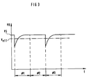
- the output voltage assigned to a digital code can be falsified due to switching peaks in the switches of the converter, as is schematically explained in FIG. 3.
- the setpoint of the output voltage VS breaks down briefly at the beginning of each first clock period ⁇ 1, which controls the weighted network, and then reaches the setpoint.
- the signal curve results in an effective output voltage V eff that is lower than the target output voltage V S.
- this phenomenon of switching peaks occurs particularly disruptively during transitions from one code to the next when several or many elements of the code change. This is the case, for example, when changing from code 01111 to code 10000. This is due to the fact that said switching peaks are strongly correlated with the individual bits. If many bits are changed, the switching tip also changes significantly. Overall, the parasitic effect results in a strong non-linearity in the characteristic curve of the D / A converter.
- a D / A converter with an undivided capacitive network will typically have an improved linearity characteristic.
- the use of an undivided capacitive network also means the use of larger capacities, which in turn means a dramatic increase in the chip area required.
- the invention has for its object to provide a digital-to-analog converter with a weighted capacitive converter network, which has a low power consumption and a good linearity characteristic with a small chip area required.
- Embodiments of the invention are characterized in the subclaims.
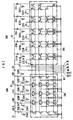
- FIG. 1 shows a block diagram of a digital-to-analog converter according to the invention.
- the converter is completely differential. This means that the circuitry of an operational amplifier OPA is symmetrical with regard to the inverting and non-inverting connections.
- the operational amplifier is connected to four capacitors C1 to C4 and two converter networks CN1 and CN2.
- the capacities C1 and C3 as well as C2 and C4 are the same.
- the arrangement works with a two-phase clock ⁇ 1 and ⁇ 2, which is generated by a clock generator, not shown.
- Input variables for the capacitance networks are the reference potentials REF1 and REF2, a reference potential VB and a control bus BST, which contains the digital information to be converted.
- the capacitance networks and the switches S1 to S4 are controlled by the clocks ⁇ 1 and ⁇ 2.
- the circuitry for the inverting input - and the non-inverted output + of the operational amplifier OPA provides the capacitance C1 between these two connections.
- the inverting input is also connected at clock ⁇ 2 via switch S1 to node CT1 of capacitance network CN1 and via switch S3 to capacitance C3.
- the capacitance C3 is with her other Connection connected to the inverted output 02 of the operational amplifier.
- the switches S1 and S3 are connected to the reference potential VB, so that the capacitance C3 and the node CT1 of the capacitance network CN1 are connected to the reference potential.
- the non-inverted output + of the operational amplifier OPA is connected to the output connection 01 and a connection of the capacitance network CN1.
- the non-inverting input + and the inverted output - of the operational amplifier OPA according to FIG. 1 are connected in a corresponding manner.
- the capacitance networks CN1 and CN2 are charged to the reference potentials REF1, REF2 and VB in accordance with the digital code present.
- These reference potentials can be the positive and negative input reference voltages, for example, if the reference potential VB is the ground potential.
- outputs 01 and 02 of the operational amplifier retain the same values as in the previous clock period. Capacitors C3 and C4 are therefore charged to the output potentials of outputs 01 and 02.
- the charges stored on the capacitance networks CN1 and CN2 are therefore not redistributed, so that the output connections 01 and 02 assume the analog voltage value that corresponds to the last digital input signal for the capacitance networks during the clock ⁇ 1. It should be added that the capacitance values can be chosen to be very low because they are limited only by the accuracy of the compensation between C1 and C3 or C2 and C4.
- FIG. 2 shows one of the two capacity networks in detail.
- Each capacity network contains a main network CNH and a partial or split network CNS.
- the two network parts are connected to one another via a coupling capacitance CK.
- Each sub-network contains weighted capacities CH1 to CH16 or CS1 to CS16.
- the network arrangement represents only one example of the invention. Of course, the capacities can also be divided differently between the subnetworks, or only an undivided network can be provided even without a subnetwork.
- the capacitances CHi of the main network are each connected to a connection at a common node K1 or to the connection CT. With their respective other connection, the weighted capacities of the main network are connected to a switch network SNH.
- the weighted capacitances CSi of the split network CNS are each connected to a second common node K2, which can be connected to the reference potential VB via a switch clocked by the clock ⁇ 1. This switch can also be omitted.
- the coupling capacitance CK lies between the two nodes K1 and K2.
- the other connections of the weighted capacities of the split network are connected to an associated switch network SNS.
- each switch network has four switch levels.
- the switches of three switch levels are controlled via the control bus BST, so that depending on the digital code applied, one of the potentials REF1, REF2 or VB can be connected to the associated connection of one of the weighted capacities of the main network or the split network.
- the fourth switch level is controlled by the clock ⁇ 2 and can connect the associated output 01 or 02 of the operational amplifier OPA to the respective connection of the weighted capacitors.
- the nodes K1 and K2 can be connected via the connection CT to one of the input connections of the operational amplifier or to the reference potential VB, as is described in FIG. 1.
- FIG. 2 also shows stray capacitances SCH1 to SCH16 for the main network CNH and stray capacities SCS1 to SCS16 for the split network CNS.
- These stray capacities result, for example, from the wiring or the technological structure of the useful capacities.
- the stray capacitances of the capacitance networks are charged either to a reference potential or to the reference potential VB.
- the stray capacitances must be reloaded to the final analog output voltages of the operational amplifier.
- the operational amplifier OPA has to provide the necessary power.
- the invention starts with the knowledge that the non-linearities described in connection with FIG. 3 are largely due to the stray capacitances.
- the invention therefore provides for additional scattering capacities to be arranged parallel to the existing scattering capacities, that the total stray capacities are weighted. With such stray capacitances weighted according to the useful capacities, the effective charge of all parasitic stray capacitances is then proportional to the output voltage at the output connections of the operational amplifier. Furthermore, an optimal coordination of the time constants from the respective switch resistance and the associated stray capacitance is possible. Because the effective charge of all stray capacitances is proportional to the output voltage, only a gain error can result, since the transient response is matched to the respective digital code.
- the teaching of the invention means that the parasitic capacitances must also be binary-weighted. This is usually not the case. This disparity between the main and the split network is usually particularly severe.
- One embodiment of the teaching according to the invention provides for the correct weighting of the parasitic stray capacitances to be achieved by connecting additional parasitic capacitances in parallel with the already existing stray capacitances until a corresponding, for example binary, weighting is achieved.
- Figure 2 shows the additional stray capacities CSA1 and CSA2 of the network SNH. Usually, the stray capacity of the least significant bit LSB is assumed. The parasitic capacitances of the higher-order bits are then doubled from stage to stage. However, since the stray capacitance of the least significant bit LSB is usually relatively large, this procedure also requires that of the stray capacitors provided in the arrangement according to FIG. 1 due to the gradual doubling of the stray capacitances low capacities overall comparatively high capacities and thus a large chip area
- the stray capacitance of a higher-value bit is assumed and the stray capacitance of the lower-weighted bits is reduced in accordance with the required weighting.
- This is made possible by providing the stray capacitances of the lower order bits with effective, i.e. negative capacitance is connected in parallel during the second clock period.
- a parallel connection of a negative effective capacitance is realized by connecting a capacitance with parallel-phase control in parallel.
Landscapes
- Engineering & Computer Science (AREA)
- Theoretical Computer Science (AREA)
- Analogue/Digital Conversion (AREA)
Applications Claiming Priority (2)
| Application Number | Priority Date | Filing Date | Title |
|---|---|---|---|
| DE4223000 | 1992-07-13 | ||
| DE4223000A DE4223000C2 (de) | 1992-07-13 | 1992-07-13 | Digital-Analog-Wandler mit gewichtetem kapazitiven Wandlernetzwerk |
Publications (3)
| Publication Number | Publication Date |
|---|---|
| EP0579025A2 true EP0579025A2 (fr) | 1994-01-19 |
| EP0579025A3 EP0579025A3 (fr) | 1995-07-12 |
| EP0579025B1 EP0579025B1 (fr) | 2000-09-06 |
Family
ID=6463088
Family Applications (1)
| Application Number | Title | Priority Date | Filing Date |
|---|---|---|---|
| EP93110323A Expired - Lifetime EP0579025B1 (fr) | 1992-07-13 | 1993-06-29 | Convertisseur numérique-analogique à réseau capacitif pondéré |
Country Status (3)
| Country | Link |
|---|---|
| US (1) | US5467089A (fr) |
| EP (1) | EP0579025B1 (fr) |
| DE (2) | DE4223000C2 (fr) |
Families Citing this family (11)
| Publication number | Priority date | Publication date | Assignee | Title |
|---|---|---|---|---|
| KR0141938B1 (ko) * | 1994-12-03 | 1998-07-15 | 문정환 | 델타 시그마 디지탈/아날로그 변환기 |
| KR100190766B1 (ko) * | 1996-06-24 | 1999-06-01 | 김영환 | 고조파 왜곡을 감소시킨 스위치드 캐패시터 디지탈-아날로그변환기 |
| US6194946B1 (en) | 1998-05-07 | 2001-02-27 | Burr-Brown Corporation | Method and circuit for compensating the non-linearity of capacitors |
| DE19936327C2 (de) * | 1999-08-02 | 2003-04-24 | Infineon Technologies Ag | Verfahren und Vorrichtung zur Durchführung von ratiometrischen Messungen unter Verwendung eines Analog/Digital- oder eines Digital/Analog-Umsetzers, Analog/Digital- oder Digital/Analog-Umsetzer, und Verfahren zum Betreiben eines Analog/Digital- oder Digital/Analog-Umsetzers |
| EP1411700B8 (fr) * | 1999-08-06 | 2006-08-30 | Matsushita Electric Industrial Co., Ltd. | Procédé et appareil d'émission de données et appareil de réception de données |
| US6294940B1 (en) | 2000-06-21 | 2001-09-25 | Infineon Technologies North America Corp. | Symmetric clock receiver for differential input signals |
| GB2388724B (en) * | 2002-05-16 | 2005-06-22 | Wolfson Ltd | Digtal-to-analogue convertor circuits |
| US7034737B1 (en) * | 2005-03-28 | 2006-04-25 | Faraday Technology Corp. | Switched capacitor circuits |
| US8238845B2 (en) | 2009-09-22 | 2012-08-07 | Broadcom Europe Limited | Radio frequency circuit |
| US9537498B2 (en) * | 2014-01-20 | 2017-01-03 | Maxlinear, Inc. | Method and system for charge compensation for switched-capacitor circuits |
| CN107800435B (zh) * | 2017-11-27 | 2023-08-25 | 广州安凯微电子股份有限公司 | 一种电容阵列寄生效应的补偿电路和抵消方法 |
Family Cites Families (11)
| Publication number | Priority date | Publication date | Assignee | Title |
|---|---|---|---|---|
| US4028694A (en) * | 1975-06-10 | 1977-06-07 | International Business Machines Corporation | A/D and D/A converter using C-2C ladder network |
| EP0078608B1 (fr) * | 1981-11-03 | 1989-08-02 | Texas Instruments Incorporated | Convertisseur analogique-numérique |
| US4568917A (en) * | 1983-06-27 | 1986-02-04 | Motorola, Inc. | Capacitive digital to analog converter which can be trimmed up and down |
| US4764753A (en) * | 1984-07-23 | 1988-08-16 | Nec Corporation | Analog to digital converter |
| JPH071870B2 (ja) * | 1984-07-31 | 1995-01-11 | 日本電気株式会社 | ディジタル/アナログ変換回路 |
| JPS6256022A (ja) * | 1985-09-02 | 1987-03-11 | Fujitsu Ltd | 電子回路 |
| US5208597A (en) * | 1988-10-13 | 1993-05-04 | Crystal Semiconductor | Compensated capacitors for switched capacitor input of an analog-to-digital converter |
| FR2641924B1 (fr) * | 1988-12-28 | 1991-05-03 | Sgs Thomson Microelectronics | Generateur de forme d'onde de signal analogique |
| US4947169A (en) * | 1989-10-24 | 1990-08-07 | Burr-Brown Corporation | Dummy/trim DAC for capacitor digital-to-analog converter |
| US5235335A (en) * | 1992-06-02 | 1993-08-10 | Texas Instruments Incorporated | Circuit and method for tuning capacitor arrays |
| US5276446A (en) * | 1992-07-01 | 1994-01-04 | Northern Telecom Limited | Analog-to-digital converter with error signal compensation and method for its operation |
-
1992
- 1992-07-13 DE DE4223000A patent/DE4223000C2/de not_active Expired - Fee Related
-
1993
- 1993-06-29 DE DE59310097T patent/DE59310097D1/de not_active Expired - Lifetime
- 1993-06-29 EP EP93110323A patent/EP0579025B1/fr not_active Expired - Lifetime
- 1993-07-13 US US08/091,172 patent/US5467089A/en not_active Expired - Fee Related
Also Published As
| Publication number | Publication date |
|---|---|
| DE4223000A1 (de) | 1994-01-20 |
| DE59310097D1 (de) | 2000-10-12 |
| US5467089A (en) | 1995-11-14 |
| EP0579025B1 (fr) | 2000-09-06 |
| EP0579025A3 (fr) | 1995-07-12 |
| DE4223000C2 (de) | 1995-04-27 |
Similar Documents
| Publication | Publication Date | Title |
|---|---|---|
| DE68913405T2 (de) | Stromquellenschaltung. | |
| DE19958049B4 (de) | Transkonduktor und Strommodus D/A-Wandler | |
| EP0396786B1 (fr) | Modulateur sigma-delta intégrable utilisant la technique des capacités commutées | |
| DE3643161C2 (de) | Verfahren und Vorrichtung zur Offsetspannungs-Korrektur in einem Analog/Digital-Umsetzer | |
| DE2855584A1 (de) | Taktgesteuerter praezisionsvergleicher | |
| DE69327602T2 (de) | Analog-/Digitalumsetzer mit Kapazitätsnetzwerk | |
| DE4223000C2 (de) | Digital-Analog-Wandler mit gewichtetem kapazitiven Wandlernetzwerk | |
| DE10153309B4 (de) | Digital-Analog-Umsetzer-Vorrichtung mit hoher Auflösung | |
| DE69018346T2 (de) | Gegentaktdoppel-Digital-zu-Analog-Konverter. | |
| DE69416661T2 (de) | Digital Analogwandler | |
| DE19722434C1 (de) | Vorrichtung zur Digital-Analog-Wandlung mit hoher Linearität | |
| EP0461282B1 (fr) | Convertisseur analogique numérique à suréchantillonnage avec filtrage de bruit en technique de capacités commutée | |
| DE3129338A1 (de) | Signalwandler | |
| EP0319609B1 (fr) | Convertisseur numérique/analogique avec commande cyclique de sources de courant | |
| DE69014481T2 (de) | Vorrichtung zur Umwandlung von elektrischen analogen unsymmetrischen Signalen in vollständig differentielle Signale. | |
| DE4320691C2 (de) | D/A-Wandler | |
| EP0442321A2 (fr) | Convertisseur analogique-numérique simultané étendu | |
| EP0736977B1 (fr) | Procédé d'autocalibrage d'un convertisseur analogique-numérique ou d'un convertisseur numérique-analogique | |
| DE3718937A1 (de) | Bipolarer a/d-wandler mit automatischer offsetkompensation | |
| DE2836948A1 (de) | Mos-analog/digital-umsetzer | |
| EP0162314A1 (fr) | Convertisseur analogique-numérique | |
| WO2000057558A2 (fr) | Circuit convertisseur numerique-analogique 1 bit | |
| DE3603841C2 (de) | Dämpfungsglied mit niedrigem Rauschverhalten und hoher thermischer Stabilität | |
| EP0133618A1 (fr) | Circuit oscillateur haute fréquence à quartz sous forme de circuit intégré monolithique | |
| DE69414538T2 (de) | Digital/Analogwandlerschaltung |
Legal Events
| Date | Code | Title | Description |
|---|---|---|---|
| PUAI | Public reference made under article 153(3) epc to a published international application that has entered the european phase |
Free format text: ORIGINAL CODE: 0009012 |
|
| AK | Designated contracting states |
Kind code of ref document: A2 Designated state(s): DE FR GB IE IT |
|
| PUAL | Search report despatched |
Free format text: ORIGINAL CODE: 0009013 |
|
| AK | Designated contracting states |
Kind code of ref document: A3 Designated state(s): DE FR GB IE IT |
|
| 17P | Request for examination filed |
Effective date: 19950804 |
|
| 17Q | First examination report despatched |
Effective date: 19970414 |
|
| GRAG | Despatch of communication of intention to grant |
Free format text: ORIGINAL CODE: EPIDOS AGRA |
|
| GRAG | Despatch of communication of intention to grant |
Free format text: ORIGINAL CODE: EPIDOS AGRA |
|
| GRAH | Despatch of communication of intention to grant a patent |
Free format text: ORIGINAL CODE: EPIDOS IGRA |
|
| 17Q | First examination report despatched |
Effective date: 19970414 |
|
| GRAH | Despatch of communication of intention to grant a patent |
Free format text: ORIGINAL CODE: EPIDOS IGRA |
|
| GRAA | (expected) grant |
Free format text: ORIGINAL CODE: 0009210 |
|
| AK | Designated contracting states |
Kind code of ref document: B1 Designated state(s): DE FR GB IE IT |
|
| REF | Corresponds to: |
Ref document number: 59310097 Country of ref document: DE Date of ref document: 20001012 |
|
| RAP2 | Party data changed (patent owner data changed or rights of a patent transferred) |
Owner name: INFINEON TECHNOLOGIES AG |
|
| REG | Reference to a national code |
Ref country code: IE Ref legal event code: FG4D Free format text: GERMAN |
|
| ITF | It: translation for a ep patent filed | ||
| GBT | Gb: translation of ep patent filed (gb section 77(6)(a)/1977) |
Effective date: 20001128 |
|
| ET | Fr: translation filed | ||
| PLBE | No opposition filed within time limit |
Free format text: ORIGINAL CODE: 0009261 |
|
| STAA | Information on the status of an ep patent application or granted ep patent |
Free format text: STATUS: NO OPPOSITION FILED WITHIN TIME LIMIT |
|
| 26N | No opposition filed | ||
| REG | Reference to a national code |
Ref country code: GB Ref legal event code: IF02 |
|
| PGFP | Annual fee paid to national office [announced via postgrant information from national office to epo] |
Ref country code: IE Payment date: 20030603 Year of fee payment: 11 |
|
| PG25 | Lapsed in a contracting state [announced via postgrant information from national office to epo] |
Ref country code: IE Free format text: LAPSE BECAUSE OF NON-PAYMENT OF DUE FEES Effective date: 20040629 |
|
| REG | Reference to a national code |
Ref country code: IE Ref legal event code: MM4A |
|
| PG25 | Lapsed in a contracting state [announced via postgrant information from national office to epo] |
Ref country code: IT Free format text: LAPSE BECAUSE OF NON-PAYMENT OF DUE FEES;WARNING: LAPSES OF ITALIAN PATENTS WITH EFFECTIVE DATE BEFORE 2007 MAY HAVE OCCURRED AT ANY TIME BEFORE 2007. THE CORRECT EFFECTIVE DATE MAY BE DIFFERENT FROM THE ONE RECORDED. Effective date: 20050629 |
|
| PGFP | Annual fee paid to national office [announced via postgrant information from national office to epo] |
Ref country code: GB Payment date: 20060615 Year of fee payment: 14 |
|
| GBPC | Gb: european patent ceased through non-payment of renewal fee |
Effective date: 20070629 |
|
| PG25 | Lapsed in a contracting state [announced via postgrant information from national office to epo] |
Ref country code: GB Free format text: LAPSE BECAUSE OF NON-PAYMENT OF DUE FEES Effective date: 20070629 |
|
| PGFP | Annual fee paid to national office [announced via postgrant information from national office to epo] |
Ref country code: FR Payment date: 20120705 Year of fee payment: 20 |
|
| PGFP | Annual fee paid to national office [announced via postgrant information from national office to epo] |
Ref country code: DE Payment date: 20120816 Year of fee payment: 20 |
|
| REG | Reference to a national code |
Ref country code: DE Ref legal event code: R071 Ref document number: 59310097 Country of ref document: DE |
|
| PG25 | Lapsed in a contracting state [announced via postgrant information from national office to epo] |
Ref country code: DE Free format text: LAPSE BECAUSE OF EXPIRATION OF PROTECTION Effective date: 20130702 |