EP0579201A1 - Photodetektor und optoelektronische integrierte Schaltung - Google Patents
Photodetektor und optoelektronische integrierte Schaltung Download PDFInfo
- Publication number
- EP0579201A1 EP0579201A1 EP93111284A EP93111284A EP0579201A1 EP 0579201 A1 EP0579201 A1 EP 0579201A1 EP 93111284 A EP93111284 A EP 93111284A EP 93111284 A EP93111284 A EP 93111284A EP 0579201 A1 EP0579201 A1 EP 0579201A1
- Authority
- EP
- European Patent Office
- Prior art keywords
- region
- electrode
- guard ring
- photodetector
- semiconductor
- Prior art date
- Legal status (The legal status is an assumption and is not a legal conclusion. Google has not performed a legal analysis and makes no representation as to the accuracy of the status listed.)
- Withdrawn
Links
Images






Classifications
-
- H—ELECTRICITY
- H10—SEMICONDUCTOR DEVICES; ELECTRIC SOLID-STATE DEVICES NOT OTHERWISE PROVIDED FOR
- H10F—INORGANIC SEMICONDUCTOR DEVICES SENSITIVE TO INFRARED RADIATION, LIGHT, ELECTROMAGNETIC RADIATION OF SHORTER WAVELENGTH OR CORPUSCULAR RADIATION
- H10F77/00—Constructional details of devices covered by this subclass
- H10F77/10—Semiconductor bodies
- H10F77/14—Shape of semiconductor bodies; Shapes, relative sizes or dispositions of semiconductor regions within semiconductor bodies
- H10F77/147—Shapes of bodies
-
- H—ELECTRICITY
- H10—SEMICONDUCTOR DEVICES; ELECTRIC SOLID-STATE DEVICES NOT OTHERWISE PROVIDED FOR
- H10F—INORGANIC SEMICONDUCTOR DEVICES SENSITIVE TO INFRARED RADIATION, LIGHT, ELECTROMAGNETIC RADIATION OF SHORTER WAVELENGTH OR CORPUSCULAR RADIATION
- H10F30/00—Individual radiation-sensitive semiconductor devices in which radiation controls the flow of current through the devices, e.g. photodetectors
- H10F30/20—Individual radiation-sensitive semiconductor devices in which radiation controls the flow of current through the devices, e.g. photodetectors the devices having potential barriers, e.g. phototransistors
-
- H—ELECTRICITY
- H10—SEMICONDUCTOR DEVICES; ELECTRIC SOLID-STATE DEVICES NOT OTHERWISE PROVIDED FOR
- H10F—INORGANIC SEMICONDUCTOR DEVICES SENSITIVE TO INFRARED RADIATION, LIGHT, ELECTROMAGNETIC RADIATION OF SHORTER WAVELENGTH OR CORPUSCULAR RADIATION
- H10F30/00—Individual radiation-sensitive semiconductor devices in which radiation controls the flow of current through the devices, e.g. photodetectors
- H10F30/20—Individual radiation-sensitive semiconductor devices in which radiation controls the flow of current through the devices, e.g. photodetectors the devices having potential barriers, e.g. phototransistors
- H10F30/21—Individual radiation-sensitive semiconductor devices in which radiation controls the flow of current through the devices, e.g. photodetectors the devices having potential barriers, e.g. phototransistors the devices being sensitive to infrared, visible or ultraviolet radiation
- H10F30/22—Individual radiation-sensitive semiconductor devices in which radiation controls the flow of current through the devices, e.g. photodetectors the devices having potential barriers, e.g. phototransistors the devices being sensitive to infrared, visible or ultraviolet radiation the devices having only one potential barrier, e.g. photodiodes
- H10F30/223—Individual radiation-sensitive semiconductor devices in which radiation controls the flow of current through the devices, e.g. photodetectors the devices having potential barriers, e.g. phototransistors the devices being sensitive to infrared, visible or ultraviolet radiation the devices having only one potential barrier, e.g. photodiodes the potential barrier being a PIN barrier
-
- H—ELECTRICITY
- H10—SEMICONDUCTOR DEVICES; ELECTRIC SOLID-STATE DEVICES NOT OTHERWISE PROVIDED FOR
- H10F—INORGANIC SEMICONDUCTOR DEVICES SENSITIVE TO INFRARED RADIATION, LIGHT, ELECTROMAGNETIC RADIATION OF SHORTER WAVELENGTH OR CORPUSCULAR RADIATION
- H10F39/00—Integrated devices, or assemblies of multiple devices, comprising at least one element covered by group H10F30/00, e.g. radiation detectors comprising photodiode arrays
- H10F39/10—Integrated devices
- H10F39/103—Integrated devices the at least one element covered by H10F30/00 having potential barriers, e.g. integrated devices comprising photodiodes or phototransistors
-
- H—ELECTRICITY
- H10—SEMICONDUCTOR DEVICES; ELECTRIC SOLID-STATE DEVICES NOT OTHERWISE PROVIDED FOR
- H10F—INORGANIC SEMICONDUCTOR DEVICES SENSITIVE TO INFRARED RADIATION, LIGHT, ELECTROMAGNETIC RADIATION OF SHORTER WAVELENGTH OR CORPUSCULAR RADIATION
- H10F77/00—Constructional details of devices covered by this subclass
- H10F77/10—Semiconductor bodies
- H10F77/12—Active materials
- H10F77/124—Active materials comprising only Group III-V materials, e.g. GaAs
- H10F77/1248—Active materials comprising only Group III-V materials, e.g. GaAs having three or more elements, e.g. GaAlAs, InGaAs or InGaAsP
-
- Y—GENERAL TAGGING OF NEW TECHNOLOGICAL DEVELOPMENTS; GENERAL TAGGING OF CROSS-SECTIONAL TECHNOLOGIES SPANNING OVER SEVERAL SECTIONS OF THE IPC; TECHNICAL SUBJECTS COVERED BY FORMER USPC CROSS-REFERENCE ART COLLECTIONS [XRACs] AND DIGESTS
- Y02—TECHNOLOGIES OR APPLICATIONS FOR MITIGATION OR ADAPTATION AGAINST CLIMATE CHANGE
- Y02E—REDUCTION OF GREENHOUSE GAS [GHG] EMISSIONS, RELATED TO ENERGY GENERATION, TRANSMISSION OR DISTRIBUTION
- Y02E10/00—Energy generation through renewable energy sources
- Y02E10/50—Photovoltaic [PV] energy
Definitions
- the present invention relates to a photodetector and an opto-electronic integrated circuit used in optical communications system. More particularly, the invention relates to a mesa type photodiode, and an opto-electronic integrated circuit in which a mesa type photodiode and a transistor are integrated on a common substrate.
- Photodiodes take an important position as photodetector for optical fiber in optical communication system.
- PIN photodiodes (as will be referred to PIN-PD) are frequently used for middle distance transmission or for small-to-middle capacity transmission, because their bias voltage is low and because high-speed PIN-PDs may be produced at a low cost.
- avalanche photodiodes (as will be referred to as APD) having the basic structure of PIN-PD are suitable for high-speed and large-capacity transmission or for long-distance transmission and widely used in such applications, because they have high sensitivity and high speed response characteristics.
- APDs Ordinary APDs normally have the mesa type structure or the guard ring structure, because a high voltage is applied thereto. Also, there are recently proposed various opto-electronic integrated circuits in which a PD and an amplifying transistor are formed on a common semiconductor substrate.
- An opto-electronic integrated circuit is formed by integrating a PIN-PD and three HEMTs (high electron mobility transistors) on a common semiconductor substrate (Goro Sasaki et al., IEEE Journal of Lightwave Technology, Vol. 7, No. 10, October 1989, p1510-p1514).
- Another opto-electronic integrated circuit is formed by integrating a PIN-PD and a plurality of HBTs (heterojunction bipolar transistors) on a common semiconductor substrate (S. Chandrasekhar et al., IEEE Photonics Technology Letters. Vol. 2, No. 7, July 1990, p505-p506).
- the PD was formed as follows in such opto-electronic integrated circuits.
- Deposited on a semiconductor substrate in the named order are an n (p) semiconductor layer in which an n-type (or p-type) impurity is added, a high-resistive semiconductor layer with no impurity added, and a p (n) semiconductor layer in which a p-type (or n-type) impurity is added.
- An n-type ohmic electrode is formed on the n-type semiconductor layer, and a p-type ohmic electrode on the p-type semiconductor layer. Further, the uppermost semiconductor layer, that is, the p (or n) semiconductor layer is removed except for the portion which is to become a light receiving area.
- the PD with the above structure is easy in production because of availability of general use techniques such as the diffusion method and the etching, but disadvantageous with a large dark current flowing between the p-type semiconductor layer and the n-type semiconductor layer. If an opto-electronic integrated circuit is constructed by integrating the PD and various transistors on a common substrate, the dark current flows into gate electrodes of the transistors to cause the shot noise, which in turn raises a problem of lowering the receiving sensitivity. In addition, a leak current might flow between elements, which increases the dark current in PD to cause the same problem.
- the opto-electronic integrated circuits of this type have a light signal detecting function. This function is achieved by detecting an increase in electric current upon incidence of light signal, which is flowing through either one of the anode electrode and the cathode electrode of PD (as will be referred to as a light signal detecting electrode) which is one not conductively connected to a gate electrode of a transistor. If the current flowing through the light signal detecting electrode in the state of no incident light signal, that is, the dark current, is large, a current change upon incidence of light signal becomes relatively small enough to cause an error in light signal detecting function. In the arrangements using the conventional PDs, the dark current negatively affects the light signal detecting function, causing a problem of inferiority thereof.
- the present invention has been accomplished taking the above problems into account. It is an object of the present invention to provide a mesa type PD having a structure capable of reducing the dark current. It is another object of the present invention to provide an opto-electronic integrated circuit having a structure capable of reducing the leak current.
- a PD of the present invention has a novel guard ring structure suitable for mesa type PD, whereby the dark current is decreased.
- the PD of the present invention comprises a first semiconductor region of either p-type or n-type, which is to be a light receiving area, and a second semiconductor region (guard ring) of the same conduction type.
- a guard ring electrode is formed on the second semiconductor region, and set at the same potential as an electrode needed to decrease the dark current.
- the dark current is desired to decrease at the anode electrode (p-type electrode) of PD
- the same potential as the anode electrode is given to the guard ring electrode.
- a leak current flowing in a p-n junction exposed on the surface of semiconductor flows into the guard ring so as to decrease the dark current at the anode electrode.
- the dark current is desired to decrease at the cathode electrode (n-type electrode)
- the same potential as the cathode electrode is given to the guard ring. Then, no electric field is applied to the p-n junction exposed on the semiconductor surface, so that no dark current flows through the cathode electrode.
- An opto-electronic integrated circuit of the present invention has the novel guard ring structure on the PD (photodetector) side, as described above, in which the anode electrode or the cathode electrode of the PD is conductively connected to a gate electrode of a field-effect transistor or to a base electrode of a bipolar junction transistor.
- the guard ring region interrupts the dark current flowing on the semiconductor surface or the leak current flowing through a channel or the like on the surface of semiconductor substrate, whereby preventing the dark current or the leak current from reaching the light receiving area.
- the thus guard ring protected anode electrode or cathode electrode of photodetector is conductively connected to a gate electrode of a field-effect transistor or to a base electrode of a bipolar junction transistor, the influence of dark current or leak current may be suppressed to improve the reliability of light signal detection operation.
- the photodetector of the present invention is so arranged that the guard ring region of the same conduction type as the first semiconductor region is disposed at a certain clearance around the first semiconductor region, which is to be a light receiving area, and that the guard ring region is kept at the same potential in operation as the light receiving area, or as the semiconductor layer of photodetector contacting with the semiconductor substrate, whereby the guard ring region interrupts the current flowing through the substrate or on the semiconductor surface so as to prevent it from reaching the light receiving area.
- This arrangement can reduce the dark current remarkably. This effect is especially outstanding in case that the substrate is InP and that at least the semiconductor layer without impurity is GaInAs.
- the dark current in the photodetector and the leak current between the photodetector and the transistor are reduced, so that the lowering of receiving sensitivity may be advantageously avoided and the error of light signal detecting function may be minimized. This can greatly improve the reliability of operation of the circuit as compared with the circuits having the conventional structures.
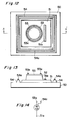
- Fig. 1 to Fig. 3 show the structure of a PD of a first type according to the present invention.
- a semiconductor substrate 10 Formed on a surface of a semiconductor substrate 10 are an n-type semiconductor layer (cathode) 11, a high-resistive semiconductor layer (i layer) 12 with no impurity added, a light receiving area (anode) 13 of p-type semiconductor on the high-resistive semiconductor layer 12, and a guard ring region 14 of p-type semiconductor surrounding the light receiving area 13 at a certain clearance.
- a cathode electrode (first electrode) 11a is formed on the surface of the n-type semiconductor layer 11, an anode electrode (second electrode) 13a on the surface of the light receiving area 13, and a guard ring electrode (third electrode)14a on the guard ring region 14.
- the PD is so arranged, though not shown, that the guard ring electrode 14a has the same potential in operation as either the anode electrode 13a or the cathode electrode 11a.
- Fig. 1 is an elevation of the PD in the first embodiment of the present invention
- Fig. 2 a cross section of the PD along A-A'
- Fig. 3 an equivalent circuit diagram thereof.
- the PD is produced by the following steps.
- the n-type semiconductor layer 11 for example of InP, GaInAsP, or GaInAs is first formed on the InP substrate 10 by the conventional OMVPE method. Then, the no-impurity-added high-resistive semiconductor layer 12 for example of GaInAs and the p-type semiconductor layer for example of InP, GaInAsP, or GaInAs are consecutively formed. After that, the p-type semiconductor layer of the uppermost layer is separated by etching into a first p-type semiconductor region 13 which is to be a light receiving area and a second p-type semiconductor region 14 which is to be a guard ring region. The second p-type semiconductor region 14 is formed as shown such that it is separated at a certain clearance around the first p-type semiconductor region 13.
- the n-type ohmic electrode 11a is formed on the upper surface of the n-type semiconductor layer 11, and the p-type ohmic electrodes 13a, 14a on the respective upper surfaces of the first and the second p-type semiconductor regions 13, 14.
- the electrode 13a and the electrode 14a, or, the electrode 11a and the electrode 14a are connected to each other as to have the same potential in operation for example by connecting the both electrodes 13a, 14a or 11a, 14a by a conductive member or by providing a conductive channel.
- the electrode 13a is arranged to have the same potential as the electrode 14a
- a leak current flowing through the p-n junction exposed on the semiconductor surface flows into the second p-type semiconductor region 14, which is the guard ring region, so that the dark current may be remarkably reduced in the first p-type semiconductor region 13.
- the electrode 11a is arranged to have the same potential as the electrode 14a
- no electric field is applied to the p-n junction exposed on the semiconductor surface, so that no dark current flows through the p-n junction exposed on the semiconductor surface.
- Fig. 4 to Fig. 6 show the structure of a PD of a second type according to the present invention.
- This PD has the same structure as the first type PD except that the n-type semiconductor and the p-type semiconductor are reversed as compared with those in Figs. 1-3.
- a p-type semiconductor layer (anode) 21 formed on a surface of a semiconductor substrate 20 are a p-type semiconductor layer (anode) 21, a high-resistive semiconductor layer (i layer) 22 with no impurity added, a light receiving area (cathode) 23 of n-type semiconductor on the high-resistive semiconductor layer 22, and a guard ring region 24 of n-type semiconductor surrounding the light receiving area 23 at a certain clearance.
- anode electrode (first electrode) 21a is formed on the surface of the p-type semiconductor layer 21, a cathode electrode (second electrode) 23a on the surface of the light receiving area 23, and a guard ring electrode (third electrode) 24a on the guard ring area 24.
- Fig. 4 is an elevation of the PD in the second embodiment of the present invention
- Fig. 5 a cross section of the PD along A-A'
- Fig. 6 an equivalent circuit diagram thereof.
- This PD is different in conduction type of the semiconductor layers or regions from the PD in the first embodiment.
- the p-type semiconductor layer 21 for example of InP, GaInAsP, or GaInAs is first formed on the InP substrate 20 by the same procedure. Then, the no-impurity-added high-resistive semiconductor layer 22 for example of GaInAs and the n-type semiconductor layer for example of InP, GaInAsP, or GaInAs are consecutively formed thereon. After that, the n-type semiconductor layer of the uppermost layer is separated into a first n-type semiconductor region 23 which is to be a light receiving area and a second n-type semiconductor region 24 which is to be a guard ring region. The second n-type semiconductor region 24 is formed as shown such that it is separated at a certain clearance around the first n-type semiconductor region 23.
- the p-type ohmic electrode 21a is formed on the upper surface of the p-type semiconductor layer 21, and the n-type ohmic electrodes 23a, 24a on respective upper surfaces of the first and the second n-type semiconductor regions 23, 24.
- the electrode 23a and the electrode 24a, or, the electrode 21a and the electrode 24a are so arranged as to have the same potential in operation in the same manner as the PD in the first embodiment.
- the mesa type PD with such structure may effectively suppress the dark current flowing the p-n junction exposed on the semiconductor surface similarly as in the first embodiment.
- Fig. 7 and Fig. 8 show the structure of such an example, in which reference numerals (30-34a) of elements correspond to those of the elements as shown in Figs. 1-6, respectively.
- the guard ring region (14, 24, 34) is arranged to have substantially the same potential in operation as either the light receiving area (13, 23, 33) or the semiconductor region (11, 21, 31), so that the dark current flowing through the semiconductor surface may be interrupted by the guard ring region (14, 24, 34) so as not to readily reach the light receiving area (13, 23, 33).
- the influence of dark current may be suppressed by conductively connecting the electrode (13a, 23a, 33a) of the light receiving region (13, 23, 33) or the electrode (11a, 21a, 31a) of the semiconductor layer (11, 21, 31) to a gate electrode of a field-effect transistor (not shown) or to a base electrode of a bipolar junction transistor (not shown).
- Fig. 9 to Fig. 11 show the structure of a PD of a third type according to the present invention.
- An n-type semiconductor layer (cathode) 41, a high-resistive semiconductor layer (i layer) 42 with no impurity added, and a light receiving area (anode) 43 of p-type semiconductor are formed in the named order on a semiconductor substrate 40.
- a guard ring region 44 of n-type semiconductor is formed at a certain clearance around the n-type semiconductor layer 41.
- a cathode electrode (first electrode) 41a is formed on the n-type semiconductor layer 41, an anode electrode (second electrode) 43a on the light receiving area 43, and a guard ring electrode (third electrode) 44a on the guard ring region 44.
- the PD is so arranged, though not shown, that the anode electrode 43a has the same potential in operation as the guard ring region 44a.
- Fig. 12 to Fig. 14 show the structure of a PD of a fourth type according to the present invention.
- This PD has the same structure as the third type PD except that the n-type semiconductor and the p-type semiconductor are reversed from those in Figs. 9-11.
- a p-type semiconductor layer (anode) 51, a high-resistive semiconductor layer (i layer) 52 with no impurity added, and a light receiving area (cathode) 53 of n-type semiconductor are formed in the named order on a semiconductor substrate 50.
- a guard ring region 54 of p-type semiconductor is formed at a certain clearance around the p-type semiconductor layer 51.
- anode electrode (first electrode) 51a is formed on the p-type semiconductor layer 51, a cathode electrode (second electrode) 53a on the light receiving area 53, and a guard ring electrode (third electrode) 54a on the guard ring region 54.
- the semiconductor layer (41, 51) and the guard ring region (44, 54) adjacent to the semiconductor substrate (40, 50) are kept substantially at the same potential, so that a leak current flowing through a channel or the like on the surface of semiconductor substrate may be interrupted by the guard ring region (44, 54) so as not to readily reach the light receiving area (43, 53). Therefore, the influence of dark current may be suppressed by conductively connecting the electrode (43a, 53a) of the light receiving area (43, 53) or the electrode (41a, 51a) of the semiconductor layer (41, 51) to a gate electrode of afield-effect transistor (not shown) or to a base electrode of a bipolar junction transistor (not shown).
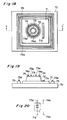
- Figs. 15-17 and Figs. 18-20 show the respective structures of PDs of fifth and sixth types in combination of the guard ring structures of the PDs as shown in Fig. 7 to Fig. 14.
- an n-type semiconductor layer (cathode) 61 and a high-resistive semiconductor layer (i layer) 62 with no impurity added are formed on a surface of a semiconductor substrate 60.
- a light receiving area (anode) 63 of p-type semiconductor is formed on the high-resistive semiconductor layer 62, and a first guard ring region 64 of p-type semiconductor is formed at a certain clearance around the light receiving region 63.
- a second guard ring region 65 of n-type semiconductor is formed at a certain clearance around the n-type semiconductor layer 61.
- a cathode electrode (first electrode) 61a is formed on the surface of the n-type semiconductor layer 61, an anode electrode (second electrode) 63a on the surface of the light receiving area 63, a first guard ring electrode (third electrode) 64a on the first guard ring region 64, and a second guard ring electrode (fourth electrode) 65a on the second guard ring region 65.
- the PD is so arranged, though not shown, that the first guard ring electrode 64a has the same potential in operation as either the anode electrode 63a or the cathode electrode 61a and that the second guard ring electrode 65a has the same potential in operation as the cathode electrode 61a.
- Figs. 18-20 also have the same structure except that the n-type semiconductor and the p-type semiconductor are reversed from those in Figs. 15-17.
- a p-type semiconductor layer (anode) 17 and a high-resistive semiconductor layer (i layer) 72 with no impurity added are formed on a surface of a semiconductor substrate 70.
- a light receiving area (cathode) 73 of n-type semiconductor is formed on the high resistive semiconductor layer 72, and a first guard ring region 74 of n-type semiconductor is formed at a certain clearance around the light receiving area 73.
- a second guard ring region 75 of p-type semiconductor is formed at a certain clearance around the p-type semiconductor layer 71.
- An anode electrode (first electrode) 71a is formed on the surface of the n-type semiconductor layer 71, a cathode electrode (second electrode) 73a on the surface of the light receiving area 73, a first guard ring electrode (third electrode) 74a on the first guard ring region 74, and a second guard ring electrode (fourth electrode) 75a on the second guard ring region 75.
- the PD is so arranged that the first guard ring electrode 74a has the same potential in operation as either the cathode electrode 73a or the anode electrode 71a and that the second guard ring electrode 75a has the same potential in operation as the anode electrode 71a.
- the PDs constructed as in Fig. 15 to Fig. 20 have the same characteristics as the PDs as shown in Fig. 1 to Fig. 14, so that the influence of dark current and leak current may be reduced thereby.
- Figs. 9-20 showed examples of mesa type PDs as described. PDs having the same structure may be also produced by ion implantation as one shown in Figs. 7 and 8 to those in Figs. 1-6.
- the PDs having the structures of Fig. 1 to Fig. 20 and transistors are formed on a common semiconductor substrate by the conventional production method.
- guard ring regions 14, 24, 34, 44, 54, 64, 74
- electrodes 14a, 24a, 34a, 44a, 54a, 64a, 74a
- the transistors may be HBTs involving FETs, or ordinary bipolar junction transistors.
- respective elements are shown by circuit symbols, and connections by circuit constitutional diagrams.
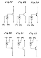
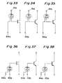
- Fig. 21 to Fig. 44 are circuit constitutional diagrams of opto-electronic integrated circuits in the embodiment of the present invention.
- Fig. 21 to Fig. 26 show examples of circuit structures involving the PD with the structure of Figs. 1-3;
- Fig. 27 to Fig. 32 examples of circuit structures involving the PD with the structure of Figs. 4-6;
- Fig. 33 to Fig. 38 examples of circuit structures involving the PD with the structure of Figs. 9-11;
- Fig. 39 to Fig. 44 examples of circuit structures involving the PD with the structure of Figs. 12-14.
- Each PD is connected to a FET in Fig.
- an electrode of each PD on the side where the guard ring region is located has the same polarity as the guard ring electrode. Further setting these electrodes at the same potential, the surface dark current flowing through the semiconductor substrate or the semiconductor surface, or the leak current flowing between the transistor and the PD flows into the guard ring region, so that the current does not affect the current flowing through a gate electrode of the transistor conductively connected to the electrode of PD. The lowering of receiving sensitivity due to the shot noise may be effectively prevented accordingly.
- Figs. 21-23, Figs. 27-29, Figs, 33-35, and Figs. 39-41 show the conditions.
- a large dark current should flow through a light signal detecting electrode (PD electrode not conductively connected to the transistor), a current change would be relatively small enough upon incidence of light signal to cause an error in light signal detecting function, as described before.
- This dark current is principally the surface dark current of PD and the leak current between elements.
- the light signal detecting electrode is set substantially at the same potential as the guard ring electrode, whereby the dark current and the leak current are reduced to minimize the error in light signal detecting function.
- Figs. 24-26, Figs. 30-32, Figs. 36-38, and Figs. 42-44 show the conditions.
- Fig. 45 is an elevation to show an embodiment of an opto-electronic integrated circuit corresponding to the circuit in Fig. 36, and Fig. 46 is a cross section thereof along A-A'.
- This opto-electronic integrated circuit is a semiconductor integrated circuit in which a PD 45 and a plurality of transistors 49 are formed on an InP substrate 30 as the PD 45 and the transistors 49 are formed as shown in Figs. 45-46.
- Figs. 45-46 show only one each of PD 45 and transistor 49 for brevity of illustration.
- the PD 45 is so constructed that an n-type semiconductor layer 41 for example of InP, GaInAsP, or GaInAs, a high-resistive semiconductor layer 42 for example of GaInAs with no impurity added, and a p-type semiconductor layer (light receiving area) 43 for example of InP, GaInAsP, or GaInAs are formed in the named order at predetermined portions on a substrate 40. Further, an n-type ohmic electrode 41a is formed on the upper surface of the n-type semiconductor layer 41, and a p-type ohmic electrode 43a on the upper surface of the p-type semiconductor layer 43. A guard ring region 44 is formed of n-type semiconductor for example of InP, GaInAsP, or GaInAs, and a guard ring electrode 44a is formed on the upper surface thereof.
- a channel is formed by surface state in an interface between the semi-insulating InP substrate 44 and a passivation film 47 as shown.
- a current flowing through this channel is the leak current. If this leak current flows into the electrodes 41a, 43a of the PD 45, it becomes a dark current.
- the guard ring region 44 interrupts the leak current.
- the guard ring electrode 44a is set at the same potential in operation as the electrode 41a on the n-type semiconductor layer 41. As so arranged, the guard ring region 44 and the n-type semiconductor layer 41 are kept at the same potential in operation, whereby the leak current may be prevented from flowing into the main structure of the PD 45.
- Fig. 47 is an elevation to show another embodiment of the opto-electronic integrated circuit corresponding to the circuit in Fig. 42, and Fig. 48 is a cross section thereof along A-A'.
- a PD 55 is so arranged that a p-type semiconductor layer 51 for example of InP, GaInAsP, or GaInAs, a high-resistive semiconductor layer 52 for example of GaInAs with no impurity added, and an n-type semiconductor layer (light receiving area) 53 for example of InP, GaInAsP, or GaInAs are formed in the named order at predetermined portions on an InP substrate 50.
- a p-type ohmic electrode 51a is formed on the upper surface of the p-type semiconductor layer 51, and an n-type ohmic electrode 53a on the upper surface of the n-type semiconductor layer 53.
- a guard ring region 54 is formed between the PD 55 and a transistor 59, which is formed of p-type semiconductor for example of InP, GaInAsP, or GaInAs.
- a guard ring electrode 54a is formed on the upper surface of the guard ring region 54.
- a channel is formed by surface state in an interface between the semi-insulating InP substrate 40 and a passivation film 57 as shown.
- a leak current flows through the channel, but may be prevented from flowing into the main structure of the PD 55 by setting the guard ring electrode 54a and the electrode 51a on the p-type semiconductor layer 51 at the same potential in operation similarly as in the third embodiment.
Landscapes
- Light Receiving Elements (AREA)
- Solid State Image Pick-Up Elements (AREA)
Applications Claiming Priority (4)
| Application Number | Priority Date | Filing Date | Title |
|---|---|---|---|
| JP4188158A JPH0637292A (ja) | 1992-07-15 | 1992-07-15 | 受光素子及び光電子集積回路 |
| JP188158/92 | 1992-07-15 | ||
| JP188159/92 | 1992-07-15 | ||
| JP4188159A JPH0637293A (ja) | 1992-07-15 | 1992-07-15 | 光電子集積回路 |
Publications (1)
| Publication Number | Publication Date |
|---|---|
| EP0579201A1 true EP0579201A1 (de) | 1994-01-19 |
Family
ID=26504758
Family Applications (1)
| Application Number | Title | Priority Date | Filing Date |
|---|---|---|---|
| EP93111284A Withdrawn EP0579201A1 (de) | 1992-07-15 | 1993-07-14 | Photodetektor und optoelektronische integrierte Schaltung |
Country Status (3)
| Country | Link |
|---|---|
| US (2) | US5365087A (de) |
| EP (1) | EP0579201A1 (de) |
| KR (1) | KR970005150B1 (de) |
Families Citing this family (9)
| Publication number | Priority date | Publication date | Assignee | Title |
|---|---|---|---|---|
| US5942788A (en) * | 1995-05-09 | 1999-08-24 | Minolta Co., Ltd. | Solid state image sensing device |
| TW504849B (en) | 1997-02-25 | 2002-10-01 | Matsushita Electric Industrial Co Ltd | Optical receiver |
| EP1115161A4 (de) * | 1998-09-18 | 2001-12-05 | Mitsubishi Cable Ind Ltd | Halbleiter photodetektor |
| US6228673B1 (en) * | 1999-05-13 | 2001-05-08 | Hughes Electronics Corporation | Method of fabricating a surface coupled InGaAs photodetector |
| JP2001358359A (ja) * | 2000-06-16 | 2001-12-26 | Nippon Sheet Glass Co Ltd | 半導体受光素子 |
| JP3822092B2 (ja) * | 2001-10-30 | 2006-09-13 | 株式会社ルネサステクノロジ | 半導体装置およびその製造方法 |
| JP2008305857A (ja) * | 2007-06-05 | 2008-12-18 | Mitsubishi Electric Corp | 光半導体装置 |
| US11309412B1 (en) * | 2017-05-17 | 2022-04-19 | Northrop Grumman Systems Corporation | Shifting the pinch-off voltage of an InP high electron mobility transistor with a metal ring |
| KR102588651B1 (ko) | 2020-11-12 | 2023-10-12 | 한국표준과학연구원 | 광 검출 소자 및 그 제조 방법 |
Citations (3)
| Publication number | Priority date | Publication date | Assignee | Title |
|---|---|---|---|---|
| EP0163295A2 (de) * | 1984-05-31 | 1985-12-04 | Fujitsu Limited | Halbleiterphotodetektor und Verfahren zu seiner Herstellung |
| DE3921028A1 (de) * | 1989-06-27 | 1991-01-10 | Siemens Ag | Avalanche-photodiode und herstellungsverfahren |
| EP0451852A1 (de) * | 1990-04-11 | 1991-10-16 | Kabushiki Kaisha Toshiba | Lawinenphotodiode mit Schutzring und Verfahren zu deren Herstellung |
Family Cites Families (7)
| Publication number | Priority date | Publication date | Assignee | Title |
|---|---|---|---|---|
| US3886579A (en) * | 1972-07-28 | 1975-05-27 | Hitachi Ltd | Avalanche photodiode |
| US4616247A (en) * | 1983-11-10 | 1986-10-07 | At&T Bell Laboratories | P-I-N and avalanche photodiodes |
| US4654678A (en) * | 1985-08-30 | 1987-03-31 | Rca, Inc. | Avalanche photodiode |
| NL8700370A (nl) * | 1987-02-16 | 1988-09-16 | Philips Nv | Stralingsgevoelige halfgeleiderinrichting. |
| JPS63224268A (ja) * | 1987-03-12 | 1988-09-19 | Mitsubishi Electric Corp | 半導体受光装置 |
| JPH0251284A (ja) * | 1988-08-12 | 1990-02-21 | Fujitsu Ltd | 半導体受光素子 |
| DE69123280T2 (de) * | 1990-04-16 | 1997-03-20 | Fujitsu Ltd | Halbleitervorrichtung mit lichtempfindlichem Element und Verfahren zu deren Herstellung |
-
1993
- 1993-07-12 US US08/089,378 patent/US5365087A/en not_active Expired - Fee Related
- 1993-07-14 EP EP93111284A patent/EP0579201A1/de not_active Withdrawn
- 1993-07-14 KR KR1019930013219A patent/KR970005150B1/ko not_active Expired - Lifetime
-
1994
- 1994-07-06 US US08/268,548 patent/US5444274A/en not_active Expired - Fee Related
Patent Citations (3)
| Publication number | Priority date | Publication date | Assignee | Title |
|---|---|---|---|---|
| EP0163295A2 (de) * | 1984-05-31 | 1985-12-04 | Fujitsu Limited | Halbleiterphotodetektor und Verfahren zu seiner Herstellung |
| DE3921028A1 (de) * | 1989-06-27 | 1991-01-10 | Siemens Ag | Avalanche-photodiode und herstellungsverfahren |
| EP0451852A1 (de) * | 1990-04-11 | 1991-10-16 | Kabushiki Kaisha Toshiba | Lawinenphotodiode mit Schutzring und Verfahren zu deren Herstellung |
Non-Patent Citations (1)
| Title |
|---|
| JOURNAL OF LIGHTWAVE TECHNOLOGY vol. 7, no. 10, October 1989, NEW YORK US pages 1510 - 1514 G.SASAKI ET AL. 'Optoelectronic integrated receivers on InP substrates by organometallic vapor phase epitaxy' * |
Also Published As
| Publication number | Publication date |
|---|---|
| US5444274A (en) | 1995-08-22 |
| US5365087A (en) | 1994-11-15 |
| KR970005150B1 (ko) | 1997-04-12 |
| KR940006291A (ko) | 1994-03-23 |
Similar Documents
| Publication | Publication Date | Title |
|---|---|---|
| US5101253A (en) | Photo sensor with monolithic differential amplifier | |
| Yamamoto et al. | Si-OEIC with a built-in PIN-photodiode | |
| US4490735A (en) | Monolithic input stage of an optical receiver | |
| US5880489A (en) | Semiconductor photodetector | |
| JP2000156520A (ja) | 受光素子およびその製造方法 | |
| JPH09121041A (ja) | InP/InGaAsモノリシック集積デマルチプレクサ、光電検出器、異質接合バイポーラ・トランジスタ | |
| US5185272A (en) | Method of producing semiconductor device having light receiving element with capacitance | |
| US5444274A (en) | Photodetector and opto-electronic integrated circuit | |
| KR19980058393A (ko) | 애벌런치 포토 다이오드 및 그의 제조방법 | |
| US6376871B1 (en) | Semiconductor device having photodetector and optical pickup system using the same | |
| EP0452801B1 (de) | Halbleitervorrichtung mit lichtempfindlichem Element und Verfahren zu deren Herstellung | |
| JP2001044484A (ja) | 回路内蔵受光素子およびその製造方法 | |
| US5268309A (en) | Method for manufacturing a photosensor | |
| US4608696A (en) | Integrated laser and field effect transistor | |
| US4314858A (en) | Method of making a fully integrated monolithic optical receiver | |
| JPS62226659A (ja) | 半導体装置 | |
| JPH0582829A (ja) | 半導体受光素子 | |
| EP0388161B1 (de) | Halbleitereinrichtung mit pin-Photodiode | |
| JPS6136713B2 (de) | ||
| KR100262409B1 (ko) | 광전자 집적 회로의 제조방법 | |
| KR100249785B1 (ko) | 수평 구조의 피아이엔 광 다이오드와 이종접합 쌍극자 트랜지스터의 결합 소자 및 그 제조방법 | |
| JP2957837B2 (ja) | 受光素子および回路内蔵受光素子 | |
| JP2670553B2 (ja) | 半導体受光・増幅装置 | |
| EP4550427A1 (de) | Photodetektor | |
| US20260130003A1 (en) | Interdigitated fingered-type spatially modulated photodetector with extra biasing for carrier acceleration in visible light communication |
Legal Events
| Date | Code | Title | Description |
|---|---|---|---|
| PUAI | Public reference made under article 153(3) epc to a published international application that has entered the european phase |
Free format text: ORIGINAL CODE: 0009012 |
|
| AK | Designated contracting states |
Kind code of ref document: A1 Designated state(s): DE FR GB NL |
|
| 17P | Request for examination filed |
Effective date: 19940718 |
|
| 17Q | First examination report despatched |
Effective date: 19950927 |
|
| STAA | Information on the status of an ep patent application or granted ep patent |
Free format text: STATUS: THE APPLICATION HAS BEEN WITHDRAWN |
|
| 18W | Application withdrawn |
Withdrawal date: 19960510 |