EP0580283A2 - Farbstrahlkopf und sein Herstellungsverfahren - Google Patents
Farbstrahlkopf und sein Herstellungsverfahren Download PDFInfo
- Publication number
- EP0580283A2 EP0580283A2 EP93304334A EP93304334A EP0580283A2 EP 0580283 A2 EP0580283 A2 EP 0580283A2 EP 93304334 A EP93304334 A EP 93304334A EP 93304334 A EP93304334 A EP 93304334A EP 0580283 A2 EP0580283 A2 EP 0580283A2
- Authority
- EP
- European Patent Office
- Prior art keywords
- substrate
- electrode
- ink jet
- jet head
- vibrating plate
- Prior art date
- Legal status (The legal status is an assumption and is not a legal conclusion. Google has not performed a legal analysis and makes no representation as to the accuracy of the status listed.)
- Granted
Links
Images










Classifications
-
- B—PERFORMING OPERATIONS; TRANSPORTING
- B41—PRINTING; LINING MACHINES; TYPEWRITERS; STAMPS
- B41J—TYPEWRITERS; SELECTIVE PRINTING MECHANISMS, i.e. MECHANISMS PRINTING OTHERWISE THAN FROM A FORME; CORRECTION OF TYPOGRAPHICAL ERRORS
- B41J2/00—Typewriters or selective printing mechanisms characterised by the printing or marking process for which they are designed
- B41J2/005—Typewriters or selective printing mechanisms characterised by the printing or marking process for which they are designed characterised by bringing liquid or particles selectively into contact with a printing material
- B41J2/01—Ink jet
- B41J2/135—Nozzles
- B41J2/14—Structure thereof only for on-demand ink jet heads
- B41J2/14314—Structure of ink jet print heads with electrostatically actuated membrane
-
- B—PERFORMING OPERATIONS; TRANSPORTING
- B41—PRINTING; LINING MACHINES; TYPEWRITERS; STAMPS
- B41J—TYPEWRITERS; SELECTIVE PRINTING MECHANISMS, i.e. MECHANISMS PRINTING OTHERWISE THAN FROM A FORME; CORRECTION OF TYPOGRAPHICAL ERRORS
- B41J2/00—Typewriters or selective printing mechanisms characterised by the printing or marking process for which they are designed
- B41J2/005—Typewriters or selective printing mechanisms characterised by the printing or marking process for which they are designed characterised by bringing liquid or particles selectively into contact with a printing material
- B41J2/01—Ink jet
- B41J2/135—Nozzles
- B41J2/16—Production of nozzles
-
- B—PERFORMING OPERATIONS; TRANSPORTING
- B41—PRINTING; LINING MACHINES; TYPEWRITERS; STAMPS
- B41J—TYPEWRITERS; SELECTIVE PRINTING MECHANISMS, i.e. MECHANISMS PRINTING OTHERWISE THAN FROM A FORME; CORRECTION OF TYPOGRAPHICAL ERRORS
- B41J2/00—Typewriters or selective printing mechanisms characterised by the printing or marking process for which they are designed
- B41J2/005—Typewriters or selective printing mechanisms characterised by the printing or marking process for which they are designed characterised by bringing liquid or particles selectively into contact with a printing material
- B41J2/01—Ink jet
- B41J2/135—Nozzles
- B41J2/16—Production of nozzles
- B41J2/1621—Manufacturing processes
- B41J2/1623—Manufacturing processes bonding and adhesion
-
- B—PERFORMING OPERATIONS; TRANSPORTING
- B41—PRINTING; LINING MACHINES; TYPEWRITERS; STAMPS
- B41J—TYPEWRITERS; SELECTIVE PRINTING MECHANISMS, i.e. MECHANISMS PRINTING OTHERWISE THAN FROM A FORME; CORRECTION OF TYPOGRAPHICAL ERRORS
- B41J2/00—Typewriters or selective printing mechanisms characterised by the printing or marking process for which they are designed
- B41J2/005—Typewriters or selective printing mechanisms characterised by the printing or marking process for which they are designed characterised by bringing liquid or particles selectively into contact with a printing material
- B41J2/01—Ink jet
- B41J2/135—Nozzles
- B41J2/16—Production of nozzles
- B41J2/1621—Manufacturing processes
- B41J2/1626—Manufacturing processes etching
- B41J2/1629—Manufacturing processes etching wet etching
-
- B—PERFORMING OPERATIONS; TRANSPORTING
- B41—PRINTING; LINING MACHINES; TYPEWRITERS; STAMPS
- B41J—TYPEWRITERS; SELECTIVE PRINTING MECHANISMS, i.e. MECHANISMS PRINTING OTHERWISE THAN FROM A FORME; CORRECTION OF TYPOGRAPHICAL ERRORS
- B41J2/00—Typewriters or selective printing mechanisms characterised by the printing or marking process for which they are designed
- B41J2/005—Typewriters or selective printing mechanisms characterised by the printing or marking process for which they are designed characterised by bringing liquid or particles selectively into contact with a printing material
- B41J2/01—Ink jet
- B41J2/135—Nozzles
- B41J2/16—Production of nozzles
- B41J2/1621—Manufacturing processes
- B41J2/1631—Manufacturing processes photolithography
-
- B—PERFORMING OPERATIONS; TRANSPORTING
- B41—PRINTING; LINING MACHINES; TYPEWRITERS; STAMPS
- B41J—TYPEWRITERS; SELECTIVE PRINTING MECHANISMS, i.e. MECHANISMS PRINTING OTHERWISE THAN FROM A FORME; CORRECTION OF TYPOGRAPHICAL ERRORS
- B41J2/00—Typewriters or selective printing mechanisms characterised by the printing or marking process for which they are designed
- B41J2/005—Typewriters or selective printing mechanisms characterised by the printing or marking process for which they are designed characterised by bringing liquid or particles selectively into contact with a printing material
- B41J2/01—Ink jet
- B41J2/135—Nozzles
- B41J2/16—Production of nozzles
- B41J2/1621—Manufacturing processes
- B41J2/1632—Manufacturing processes machining
-
- B—PERFORMING OPERATIONS; TRANSPORTING
- B41—PRINTING; LINING MACHINES; TYPEWRITERS; STAMPS
- B41J—TYPEWRITERS; SELECTIVE PRINTING MECHANISMS, i.e. MECHANISMS PRINTING OTHERWISE THAN FROM A FORME; CORRECTION OF TYPOGRAPHICAL ERRORS
- B41J2/00—Typewriters or selective printing mechanisms characterised by the printing or marking process for which they are designed
- B41J2/005—Typewriters or selective printing mechanisms characterised by the printing or marking process for which they are designed characterised by bringing liquid or particles selectively into contact with a printing material
- B41J2/01—Ink jet
- B41J2/135—Nozzles
- B41J2/16—Production of nozzles
- B41J2/1621—Manufacturing processes
- B41J2/164—Manufacturing processes thin film formation
- B41J2/1642—Manufacturing processes thin film formation thin film formation by CVD [chemical vapor deposition]
-
- B—PERFORMING OPERATIONS; TRANSPORTING
- B41—PRINTING; LINING MACHINES; TYPEWRITERS; STAMPS
- B41J—TYPEWRITERS; SELECTIVE PRINTING MECHANISMS, i.e. MECHANISMS PRINTING OTHERWISE THAN FROM A FORME; CORRECTION OF TYPOGRAPHICAL ERRORS
- B41J2/00—Typewriters or selective printing mechanisms characterised by the printing or marking process for which they are designed
- B41J2/005—Typewriters or selective printing mechanisms characterised by the printing or marking process for which they are designed characterised by bringing liquid or particles selectively into contact with a printing material
- B41J2/01—Ink jet
- B41J2/135—Nozzles
- B41J2/16—Production of nozzles
- B41J2/1621—Manufacturing processes
- B41J2/164—Manufacturing processes thin film formation
- B41J2/1645—Manufacturing processes thin film formation thin film formation by spincoating
-
- B—PERFORMING OPERATIONS; TRANSPORTING
- B41—PRINTING; LINING MACHINES; TYPEWRITERS; STAMPS
- B41J—TYPEWRITERS; SELECTIVE PRINTING MECHANISMS, i.e. MECHANISMS PRINTING OTHERWISE THAN FROM A FORME; CORRECTION OF TYPOGRAPHICAL ERRORS
- B41J2/00—Typewriters or selective printing mechanisms characterised by the printing or marking process for which they are designed
- B41J2/005—Typewriters or selective printing mechanisms characterised by the printing or marking process for which they are designed characterised by bringing liquid or particles selectively into contact with a printing material
- B41J2/01—Ink jet
- B41J2/135—Nozzles
- B41J2/16—Production of nozzles
- B41J2/1621—Manufacturing processes
- B41J2/164—Manufacturing processes thin film formation
- B41J2/1646—Manufacturing processes thin film formation thin film formation by sputtering
-
- B—PERFORMING OPERATIONS; TRANSPORTING
- B41—PRINTING; LINING MACHINES; TYPEWRITERS; STAMPS
- B41J—TYPEWRITERS; SELECTIVE PRINTING MECHANISMS, i.e. MECHANISMS PRINTING OTHERWISE THAN FROM A FORME; CORRECTION OF TYPOGRAPHICAL ERRORS
- B41J2/00—Typewriters or selective printing mechanisms characterised by the printing or marking process for which they are designed
- B41J2/005—Typewriters or selective printing mechanisms characterised by the printing or marking process for which they are designed characterised by bringing liquid or particles selectively into contact with a printing material
- B41J2/01—Ink jet
- B41J2/135—Nozzles
- B41J2/14—Structure thereof only for on-demand ink jet heads
- B41J2002/14379—Edge shooter
-
- B—PERFORMING OPERATIONS; TRANSPORTING
- B41—PRINTING; LINING MACHINES; TYPEWRITERS; STAMPS
- B41J—TYPEWRITERS; SELECTIVE PRINTING MECHANISMS, i.e. MECHANISMS PRINTING OTHERWISE THAN FROM A FORME; CORRECTION OF TYPOGRAPHICAL ERRORS
- B41J2202/00—Embodiments of or processes related to ink-jet or thermal heads
- B41J2202/01—Embodiments of or processes related to ink-jet heads
- B41J2202/03—Specific materials used
-
- B—PERFORMING OPERATIONS; TRANSPORTING
- B41—PRINTING; LINING MACHINES; TYPEWRITERS; STAMPS
- B41J—TYPEWRITERS; SELECTIVE PRINTING MECHANISMS, i.e. MECHANISMS PRINTING OTHERWISE THAN FROM A FORME; CORRECTION OF TYPOGRAPHICAL ERRORS
- B41J2202/00—Embodiments of or processes related to ink-jet or thermal heads
- B41J2202/01—Embodiments of or processes related to ink-jet heads
- B41J2202/11—Embodiments of or processes related to ink-jet heads characterised by specific geometrical characteristics
Definitions
- the present invention relates to an ink jet head of an important portion of an ink jet recording apparatus, having its drive system of static electricity, for outletting ink drops when a recording is necessary and attaching the drops onto a recording paper face, and a manufacturing method of the ink jet head effectively attaining a purpose of the present invention.
- the ink jet recording apparatus has many merits or advantages, such as very small sound during a recording, high speed printing, high flexibility on ink, and use of low cost plain paper. According to the recent trend, an ink jet recording apparatus of an ink-on-demand system emitting ink drops only when recording is necessary mainly has been employed because it is not necessary to recover ink drops not used to the recording.
- the ink jet head of an ink-on-demand has a drive means using a piezoelectric element.
- the ink jet head heats ink and generates bubbles and pressure making ink drops emit.
- the ink jet head using a piezoelectric element it is necessary to carry out a complicated process of attaching a chip of piezoelectric element to the vibrating plates used to generate pressure in a pressure chamber in a manufacturing process the ink jet head.
- the recent ink jet recording apparatus necessitates a printing of a high speed and a high appearance quality.
- it has been necessary to make the ink jet nozzles of a multi-nozzle and a high density of the nozzle necessitating a fine manufacturing of piezoelectric elements and attachment of the fine elements to respective vibrating plates.
- the drive means is constructed by a thin membrane resistance heater element having no problem of the conventional piezoelectricity element apparatus above.
- the drive means is suffered or damaged by high speed repetition of heating and cooling and shock of bursting bubbles shortening a lifetime of the ink jet head.
- the ink jet head recording apparatus of the application has problems to be solved in order to still improve such merits above.
- the first problem concerns a vibrating plate constituting an ink limiting or discharging chamber, and a gap between the vibrating plate and an electrode for driving the vibrating plate.
- emitting pressure to be generated by the same pressure is very low comparing to that of the jet head of piezoelectric element.
- generated pressure is proportional to a square of an inverse number of the gap distance, it is necessary, in order to prevent printing quality from scattering, to hold the size of gap in the predetermined range with a very high precision.
- Emitting pressure is proportional to a cube of the thickness of the vibrating plate.
- emitting pressure is proportional to fifth power of an inverse number of the short side length of the square-shaped vibrating plate, thereby even small scattering or variations of the size of the vibrating plate affects an ink emitting characteristic very much.
- the third problem concerns a head manufacturing method for realizing or attaining a size precision of the high precised gap and the vibrating plate mentioned above.
- An anode bonding method has been used to joint the substrates of such kind to each other.
- a boro-silicated gas substrate is connected to a cathode side
- a silicon substrate provided with nozzles and the vibrating plate is connected to an anode side and a 500V voltage is impressed to them at a temperature 300°C.
- Na ions contained in the boro-silicated glass move to cathode side by an electric field, thereby a very strong static electricity attractive force is generated between the boro-silicated glass andthe silicon and they are contacted.
- the electrode melts and the melt is attached to the vibrating plate generating a short circuit.
- the vibrating plate is fixed through its circumference after it is deformed due to the electric field generated while an anode connecting.
- the ink jet head of the present invention has a single or plural nozzle holes for emitting ink drops, an emitting chamber led to respective nozzle holes, a vibrating plate constituting at least one wall of the emitting chamber, a drive means for generating a deformation in the vibrating plate, wherein the drive means consists of an electrode for deforming the vibrating plate by static electricity force.
- an opposing obstacle between the vibrating plate and the electrode is made 0.05 ⁇ m or more than 0.05 ⁇ m, and 2.0 ⁇ m or less than 2.0 ⁇ m.
- the opposing distance holding means of the ink jet head of the present invention is a dent for a vibrating chamber forced on the first substrate of the vibrating plate, or another dent for electrode mounting, which is formed in the second substrate of the electrode, or both dents.
- the first substrate and the second substrate respectively are mono-crystal silicon substrates, and a SiO2 membrane formed on at least one face of the connecting portion of both substrates constitutes a holding means for the opposing gap or distance.
- the SiO2 membrane by thermal oxidized membrane of silicon, or the SiO2 membrane can be produced by spattering process a sintering process of inorganic silicon compound or a CVD process vaperizing process, Sol-Gel process, thermal oxidation process or others.
- the electrode is formed by p-type or n-type impurities.
- the electrode is covered by a dielectric membrane with a gap formed between the electrode and the vibrating plate.
- the method comprises at least one of the steps of pattern-forming of SiO2 membrane of a predetermined thickness on the connecting face of the first silicon substrate forming the vibrating plate excepting its part for the vibrating plate, and of pattern-forming of SiO2 membrane of a predetermined thickness on the connecting face of the second silicon substrate forming the electrode excepting its part for the electrode, and of anode connecting the first and the second silicon substrates through the SiO membrane by means of a Si direct connecting process.
- the method has a vibrating plate forming step carried by an alkali anisotropy etching to be done on the first silicon substrate, and a step for manufacturing the electrode consisting of p-type or n-type impurities by carrying out a doping on the second silicon substrate.
- the ink jet head has the second electrode integrally formed in the vibrating plate so as to keep the gap between the opposing distance or parts.
- the second electrode is formed with p-type or n-type impurities.
- the gap distance holding means of the head is a gap spacer formed by a boro-silicated glass membrane previously formed on at least one face of the connecting portion of the first and the second substrates.
- the boro-silicated glass membrane is produced by a spattering process.
- the vibrating plate is formed by a n-type impurities layer or a high density p-type impurities layer.
- a driving wiring layer containing the second electrode is formed by a high density p-type impurities layer.
- the first substrate is a silicon substrate of crystal face direction (110) and made by epitaxially growing a n-type impurities layer on a p-type silicon substrate.
- Another embodiment of the ink jet manufacturing method has a step of forming a n-type impurity layer on a p-type silicon substrate, and a step of forming the vibrating plate by carrying out an electric chemical anisotropy etching process on the silicon substrate.
- the anode bonding method for bonding the first substrate having the vibrating plate formed thereon to the second substrate having the electrode formed thereon so as to drive the vibrating plate has a step for controlling in a manner that a voltage difference between the vibrating plate and the electrode when the anode bonding process is done.
- a potential of the electrode is made identical with that of the vibrating plate.
- the annode bonding process for anode bonding the first substrate having the vibrating plate formed thereon and the second substrate having the electrode driving the vibrating plate comprises a step for forming a common electrode adapted to be connected to respective electrode on the second substrate, a step for controlling or decreasing a potential between the vibrating plate and the common electrode when these first and second substrates are anode-connected, and a step for separating the common electrode from the electrode driving the vibrating plate after the anode-connecting process.
- the gap between the vibrating plate and the electrode has a passage led to the outside before the first substrate provided with the vibrating plate formed thereon and the second substrate provided with the electrode are anode bonding and the outlet of the passage is sealed by the sealing member after the anode connection process is done.
- the opposed distance holding mean is a photo-sensitive resin layer or adhesive agent layer of a pattern around the electrode.
- impressing a pulse voltage to the electrode functions static electricity attractive force or repelling force between the electrode and the vibrating plate opposed to the electrode, deforming the vibrating plate and emitting ink drops through the nozzle holes. Because of a restriction of the opposed gap or distance between the vibrating plate and the electrode, it is possible to drive the ink jet head with a low voltage, and emitting speed and emitting volume of ink drops are stable attaining very high quality of printing.
- the gap length or distance of the opposed gap is confirmed by experiments.
- the reasons why the gap length is 0.05 ⁇ m or more than 0.05 ⁇ m are the volume of emitted ink drop is not enough to print a letter when the length is less than 0.05 ⁇ m, and the vibrating plate contact with the electrode breaking the electrode.
- the gap length is 2.0 ⁇ m or less than that is caused by driving voltage. If the length is more than 2.0 ⁇ m, it is impossible to attain substantive high capacity of the ink jet head.
- the gap length restricted as described above there are a dent for the vibrating chamber, a dent for mounting the electrode, SiO2 membrane formed on the connecting face of the substrate to be connected, boro-silicated glass membrane, or photo-sensitive resin layer or adhesive agent layer.
- the necessary gap length is held by these dents or membranes.
- SiO membrane or boro-silicated glass membrane is used, it is possible to control the thickness the membrane with a high precision and to equalize the vibration characteristic of the vibrating plate resulting accordingly in a uniformed quality of printing.
- the second electrode is integrally formed on the vibrating plate, electric resistance of the second electrode lowers improving driving frequency of the ink jet head of the present invention and resulting in a high speed printing.
- the first substrate forming the vibrating plate is formed by a silicon substrate of crystal face direction (110), it is possible to make a wall face of the cavity perpendicular to the face of the silicon substrate due to an etching the miniaturize the pitch distance of the nozzles, and to attain a small and high density of the ink jet head.
- the vibrating plate is made of a high density p-type impurity layer, it is possible to improve the driving frequency and crosstalk of the ink jet head.
- the potential between the vibrating plate and the electrode is controlled to lower, for example to equalize both potentials of them during an anode connection between the first substrate provided with the vibrating plate formed thereon and the second substrate provided with the electrode formed thereon being anode bonded, it is possible to prevent discharging between the vibrating plate and the electrode or dispersion of electric field when they are anode bonded and peeling-off of the dielectric membrane due to static electricity attractive force.
- the passage on the gap portion between the vibrating plate and the electrode Due to a formation of the passage on the gap portion between the vibrating plate and the electrode so as to lead to the outside, it is possible to prevent pressure in the gap space owing to heating process of the anode-connection from rising, keep the gap length at the predetermined one, and prevent a generation of remaining stress in the vibrating plate and a contact between the vibrating plate and electrode.
- the outlet of the passage is sealed by the sealing member after the anode-connection process is done and the temperature of the whole construction of the ink jet head lowers to a room temperature preventing dust from invading into the gap space.
- Fig. 1 is an exploded perspective view showing the ink head according to the first embodiment of the present invention and a part of the head is shown in a section.
- the first embodiment is the ink jet head of an edge ink jet type wherein ink drops emit through a nozzle hole formed at an end portion of the substrate.
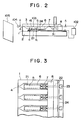
- Fig. 2 is a sectional elevation of the whole structure of the assembled ink jet head, and
- Fig. 3 is a section along the arrows A-A of Fig. 2.
- the ink jet head 10 of the embodiment has a laminated structure of three substrates 1, 2 and 3, respectively have a construction as described below.
- the first middle substrate 1 is of a silicon one and has a plurality of nozzle grooves 11 placed at an end of the face of the substrate 1 and at a regular interval in parallel to each other ending with plurality of nozzle holes 4, a plurality of dents or concave portions 12 constituting emitting chambers 6 respectively led to each nozzle grooves 11 and having their bottom walls of the vibrating plates 5, a plurality of their grooves 13 of ink flowing inlets constituting orifices 7 at rear portions of the concave portions 12, and a dent or concave portion 14 of a common ink cavity 8 for supplying ink to respective emitting chambers 6. Also, there are dents 15 on the lower portions of the vibrating plates 5, which dents constituting vibrating chambers 9. Electrodes are mounted in the vibrating chambers 9 as described below.
- a distance holding means is constituted by the dents 15 used as vibrating chambers formed on the bottom face of the first substrate 1 in order to make the opposed distance between the vibrating plate 5 and an electrode oppositely placed to the plate, or a length of the gap portion (see Fig 2, hereinafter referred to as gap length) identical with a difference between a depth of the dent 15 and a thickness of the electrode.
- the dent 15 is etched to have a depth of 0.6 ⁇ m.
- a pitch of the nozzle grooves 11 is 0.72mm and a width of the nozzle groove 11 is 70 ⁇ m.
- the second substrate 2 attached to the bottom face of the first substrate 1 is made of (boro-silicated glass) and these attached substrates 1 and 2 constitute a vibrating chamber 9.
- gold of a pattern similar to the shape of the vibrating plate is spatted with a thickness of 0.1 ⁇ m in order to obtain a golden pattern of a shape almost identical with that of the vibrating plate 5.
- a boro-silicated glass spattering film covers the second substrate 2 excepting the electrode terminals 23 with a thickness of 0.2 ⁇ m.
- the dielectric layer 24 may consist of silicone compound.
- the third substrate 3 attached to an upper face of the first substrate 1 is made of boro-silicated glass identical with that of the second substrate 2. Combining the third substrate 3 forms the nozzle hole 4, the emitting chamber 6, the orifice 7, and the ink cavity 8.
- the substrate 3 has an ink supply opening 31 led to the ink cavity 8.
- the ink supply opening 31 is connected to an ink tank (not shown) through a connecting pipe 32 and a tube 33.
- the first substrate 1 and the second substrate 21 are anode bonding by impressing a voltage of 500V at a temperature 300°C to them.
- the first substrate 1 and the third substrate 3 are connected and the ink jet head shown in Fig. 2 is assembled.
- a difference between the depth of the dent 15 and the thickness of the electrode 21 is the gap length between the vibrating plate 5 and an electrode 21 on the second substrate 2 is made 0.5 ⁇ m.
- a space distance G1 between the vibrating plate 5 and the dielectric layer 24 on the electrode 21 is made 0.3 ⁇ m.
- oscillation circuit 102 is connected between the substrate 1 and a terminal 23 of the electrode 21 through a wire 101 in order to form an ink jet recording apparatus.
- Ink 103 is supplied to an interior of the substrate 1 from an ink tank (not shown) through the ink supply port 31 and the ink cavity 8 and the emitting chamber 6, etc. are filled with ink.
- an ink drop 104 is emitted from the nozzle hole 4 onto a recording paper 105.
- pulse voltage of 0V to 70V is impressed to the electrode 21 by the oscillation circuit 102 and a surface of the electrode 21 is charged plus or positive. Then, a lower face of the opposed vibrating plate 5 is charged negative. As a result, the vibrating plate 5 bends downward by sucking effect of static electricity. Next, the electrode 21 is made off, the vibrating plate 5 returns to its original position. Thus, pressure in the emitting chamber 6 abruptly rises and an ink drop 104 is emitted onto the recording paper 105 through the nozzle hole 4. Then, the vibrating plate 5 again bends downward and ink 103 is supplied to the emitting chamber 6 from the ink cavity 8 through the orifice 7.
- the ink jet head 10 of the present invention is assembled to a printer as shown at Fig. 35, 5 KHz drive power flies ink drops with a speed 7m/sec onto the recording paper. Resulting printing efficiency was very good with such low voltage for driving or flying ink drops, in Fig. 35, numeral 300 is a platen, 301 is a ink tank, and 302 is a carriage of the ink head 10. When the gap length between the vibrating plate 5 and the electrode 21 is 2.5 ⁇ m, drive voltage was unpractically more than 250V.
- Fig. 4 is an exploded perspective view of the ink jet head according to the second embodiment of the present invention and a part of the ink jet head is shown by breaking in section.
- the ink jet head shown is of a face ink jet type having nozzle holes formed at a face portion of a substrate, through which holes ink drops emit.
- Fig. 5 shows a sectional side elevation of the whole construction of an assembled ink jet head according to the present invention and
- Fig. 6 shows a sectional view taken along a B-B line in Fig. 2.
- the part or members of the ink jet head identical with or similar to that of the embodiment 1 will be explained with the identical reference numbers of the embodiment 1.
- the ink jet head 10 of the second embodiment is adapted to emit ink drops through the nozzle holes 4 formed in a face of the third substrate 3.
- the first substrate 1 of this second embodiment is made of a silicon of crystal face direction (110) of a thickness 380 ⁇ m.
- the bottom wall of the dent 12 constituting the emitting chamber 6 is a vibrating plate 5 of a thickness 3 ⁇ m.
- the second substrate 2 attached to the bottom face of the first substrate 1 is made of Boro-Silicated glass as that of the first embodiment.
- the gap length G is formed on the second substrate by a dent 25 formed by an etching process of 0.5 ⁇ m in order to mount the electrode 21.
- the dent 25 is made in a pattern larger a little than a shape of the electrode in order to mount the electrode 21, lead 22, terminal 23 in the dent 25.
- the electrode 21 is made by spattering ITO of 0.1 ⁇ m thickness in the dent 25 to form ITO pattern, and gold used to bondings are spattered only on the terminal 23.
- the dielectric layer 24 is drawn as a flat shape. In fact, the dielectric layer 24 has dents 25 formed in the flat surface.
- the gap length is 0.4 ⁇ m and the space distance G1 is 0.3 ⁇ m after an anodic bonding.
- the third substrate 3 attached to the top face of the first substrate 1 is made of SUS plate of a thickness 100 ⁇ m.
- the ink supply port 31 is formed so as to be led to the dent or concave 14 of the ink cavity.
- the ink jet head 10 of the third embodiment When the ink jet head 10 of the third embodiment is used and a plate voltage of OV to 100V is impressed from the oscillation circuit 102 to the electrode 21, a good printing efficiency corresponding to that of the first embodiment is obtained.
- the ink jet head provided with a gap length G of 2.3 ⁇ m When the ink jet head provided with a gap length G of 2.3 ⁇ m is used, the driving voltage becomes more than 250V, thereby the ink jet head is not practical in the printer.
- Fig. 7 shows an exploded perspective view of the ink jet head according to the third embodiment of the present invention and a part of the head is shown in section.
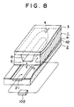
- Fig. 8 is an enlarged perspective view of a part of the ink jet head.
- the gap length holding means is formed by SiO2 membranes 41 and 42, respectively and previously formed at the space between the first substrate 1 and the second substrate 2.
- These SiO2 membranes 41 and 42 function as gap spacers.
- the first substrate 1 is made of a single crytal silicon wafer of a crystal face direction (100).
- the SiO2 membrane 41 of, for example, a thickness 0.3 ⁇ m is formed.
- the second substrate 2 is made of a single crystal silicon wafer of a crystal face direction (100).
- SiO2 membrane 42 of, for example, 0.2 ⁇ m is formed on the upper face of the second substrate 2 except the electrode 21.
- the gap length between these substrates 1 and 2 becomes 0.5 ⁇ m (see Fig. 8).
- Fig. 9 shows the manufacturing steps of the first substrate according to the third embodiment of the present invention.
- both faces of the silicon wafer of a crystal face direction (100) are mirror-polished in order to make a silicon substrate 51 of a thickness 200 ⁇ m (see Fig. 9(a)).
- the silicon substrate 51 is treated with thermal oxidization treatment in oxygen and steam atmosphere of a temperature 1100°C for 4 hours in order to form a SiO2 membranes 41a and 41b of a thickness 1 ⁇ m on both the faces of the silicon substrate 51 (see Fig. 9(b)).
- SiO2 membranes 41a and 41b function as an anti-etching material.
- a photo-resist pattern (not shown) having a pattern of nozzle 4, emitting chamber 6, orifice 7 and ink cavity 8 is formed.
- the exposed portion of the SiO2 membrane 41a is etched by fluoric acid etching agent and the photo-resist pattern is removed (see Fig. 9(c)).
- the silicon substrate 51 is arisotrophy-etched by alkali agent.
- alkali such as kalium hydroxide solution and hydradin, etc.
- difference between etching speeds on various crystal faces of the single crystal silicon is large, thereby it is possible to carry out arisotrophy etching on them.
- the etching speed of (111) crystal face is the least or the lowest, the crystal face (111) is remained after the etching process is finished.
- caustic potash solution containing isopropyl alcohol is used in the etching treatment. Because mechanical deformation characteristics of the vibrating plate is determined by each size or measurement of the vibrating plate, the design size of every part of the vibrating plate is determined with reference to ink emitting characteristics necessary to the ink jet head of the present invention. According to the third embodiment, a width h of the vibrating plate 5 is 500 ⁇ m and its thickness is 30 ⁇ m (see Fig. 10).
- (111) face crosses structurally with (100) face of the substrate at an angle of about 55°, so that when the sizes of the vibrating plate to be formed in the silicon substrate of (100) face direction are determined, the mask pattern size of anti-etching material is primarily determined with reference to the thickness of the first substrate.
- the width d of the top opening of the emitting chamber 6 is determined 740 ⁇ m and an etching treatment of 170 ⁇ m width is done, so that the vibrating plate 5 of a width h of 500 ⁇ m and a thickness t of 30 ⁇ m is obtained.
- (111) face is a little etched or undercut and the size d shown in Fig.
- the mask pattern width d 1 small by a part corresponding to that of (111) face 12a undercut, so that it is 730 ⁇ m in the third embodiment of the present invention and the predetermined length (170 ⁇ m) is etched by alkali etching solution (see Fig. 9(d)).
- SiO2 membrane 41b on the bottom face of the silicon substrate 51 is patterned.
- the thickness of the SiO2 membrane 41b was 1 ⁇ m at the stage Fig. 9(b).
- the SiO2 membrane 41b is etched by alkali solution and its thickness decreased to 0.3 ⁇ m.
- an etching rate of the SiO2 membrane is very small, so a reproductivity of decrease in a thickness of the SiO2 membrane 41b is good and uniform.
- a photo-resist pattern (not shown) of a shape corresponding to the vibrating plate 5 is formed on the SiO2 membrane 41b(41), the exposed portion of the SiO2 membrane 41b is etched by fluoric acid etching solution so as to remove the photo-resist pattern. Simultaneously, all material of the SiO2 membrane 41a remained on the upper face of the substrate 51 is removed (see Fig. 9(e)).
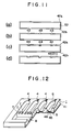
- both the faces of a n-type silicon substrate 52 of (100) face direction are mirror-polished and heat and oxidization treatment is done on the substrate 52 in oxygen and steam atmosphere at 1100° C for a predetermined time in order to form the SiO2 membranes 42a and 42b on both the faces of the silicon substrate 52 (see Fig. 11(a)).
- a photo-resist pattern (not shown) corresponding to the shape of the electrode 21 is formed on the upper SiO2 membrane 42a and the exposed portion of the SiO2 membrane 42a is etched by fluoric acid etching solution to remove the photo-resist pattern (see Fig. 11(b)).
- the exposed Si portion 43 of the silicon substrate 52 is boron-doped.
- a boron-doping process is shown below.
- the silicon substrate 52 is held in a quartz tube through a quartz holder, steam with bubbled BBr3 of N2 carriers is led together with O2 into the quartz tube.
- the substrate 52 is lightly etched by fluoric acid etching agent, then driven-in within O2.
- the exposed part of Si 43 is a p-type layer 44 (see Fig. 11(c)).
- the p-type layer 44 functions as the electrode 21 as shown in Fig. 7.
- the thickness of the SiO2 membranes 42a and 42b on the upper face of the silicon substrate 52 increases, so in the third embodiment the thickness of the SiO2 membrane 42a is made to increase to 0.2 ⁇ m.
- a photo-resist pattern (not shown) corresponding to the shape of the p-type layer 44 (electrode 21) is formed and the exposed ones of the SiO2 membrane 42a are etched by fluoric acid etching agent removing them (see Fig. 11(d)).
- the second substrate 2 shown in Fig. 7 is obtained.
- the size of the gap length G between the vibrating plate 5 and the electrode 21 is determined to 0.5 ⁇ m on the basis of an ink emitting characteristic of the ink jet head. Because the thickness of the SiO2 membrane 41b of the first substrate 1 is 0.3 ⁇ m as mentioned above, the process is carried out so that the thickness of the SiO2 membrane 42a in the step of Fig. 11 (c) becomes 0.2 ⁇ m.
- the substrate 1 and 2 formed according to the steps above are joined by a Si-Si direct connecting method making the head construction as shown enlargely in Fig. 8. The joining steps will be described.
- the silicon substrate 1 is washed with a mixture of sulfuric acid and hydrogen peroxide of 100°C, then positions of the corresponding patterns of both the substrates 1 and 2 are matched, and finally they are piled each other. After that, both the subtrates 1 and 2 are thermally treated at a temperature of 1100°C for one hour obtaining firm combination of them.
- the sizes of the gap length G of one hundred ink jet heads manufactured are scattered in 0.50 ⁇ 0.05 ⁇ m. and the thicknesses of the vibrating plates are scattered or distributed in a range of 30.0 ⁇ 0.8 ⁇ m.
- ink jet heads are driven with 100V and 5 KHz, ink drop emitting speeds are scattered in a range of 8 ⁇ 0.5 ⁇ m/sec. and ink drop volumes are distributed in a range of (0.1 ⁇ 0.01) x 10 ⁇ 6 cc. In a practical printing test of the one hundred ink jet heads, good results of printing are obtained.
- a gaseous process using BBr3 forms a p-type layer and the electrode 21.
- the p-type layer forming method includes ones, such as an ion injection method, a spin-coating method in which coating agent B2O3 scattered in inorganic solvent is spinned, and other method using a distribution source of BN (Boron nitrogen) plate. It is possible to use other elements in group III, such as A1, Ga in order to form p-type layers.
- the electrode 21 a n-type layer supposing that the silicon substrate 2 is a p-type substrate.
- various doping methods are used, that is V group elements such as P, As, Sb and the like are doped making the electrode 21.
- the SiO2 membranes 41 and 42 form the gap portions.
- one of the membranes 41 and 42 may have the necessary length of the gap and another membrane may be removed by fluoric acid etching agent in a Si-Si direct connecting process obtaining the gap portion of the same material.
- the SiO2 membrane of the gap spacer is used as an etching mask when an alkali arisotrophy etching process is done and the size of the membrane decreases, so that the face condition a little deteriorates while an etching step.
- a thermal oxidization process is used to form SiO2 membrane of a necessary thickness obtaining a suitable gap spacer.
- the gap length is determined temporarily to 0.5 ⁇ m.
- Si thermal oxidized membranes can be manufactured precisely and easily until their thicknesses reach 1.5 ⁇ m, only controlling the thickness of the Si thermal oxidized membranes of the gap spacers according to the specification in case that the specified size of the gap length is 0.05 to 2.0 ⁇ m enables to obtain an ink jet head provided with the gap portion having a precise measurement similar to that of the third embodiment.
- Fig. 12 shows a partly-broken perspective view of the first substrate used to the ink jet head according to the fourth embodiment of the present invention.
- the second substrate and the third substrate on which electrodes are formed are identical with that of the third embodiment of the present invention and the explanations for them are omitted from the specification.
- a second electrode 46 consisting of a p-type or n-type impurity layer is formed on the gap opposed face 45 of the vibrating plate 5 as shown in Fig. 12 in order to improve frequency characteristic of the oscillation circuit or crosstalk when the ink jet head is driven.
- the gap length G of the fourth embodiment is the space distance between the second electrode 46 and the electrode 21 on the second substrate (see Fig. 7).
- the distance holding means is constructed by the SiO2 membrane 41 formed on the bottom face of the first substrate 1 in a manner described below and the second substrate of the third embodiment. In this case too, it is possible to obtain the gap length G by only one of the SiO2 membranes.
- both the sides of a silicon wafer of n-type (100) face direction are mirror-polished to manufacture a silicon substrate 53 of a thickness 200 ⁇ m (see Fig. 13(a)), the silicon substrate 53 is thermally oxidization-treated in an oxygen-steam atmosphere at 1100°C for 4 hours in order to form SiO2 membranes 41a and 41b of thickness 1 ⁇ m on both the faces of the silicon substrate 53 (see Fig. 13b)).
- a photo-resist pattern (not shown) corresponding to the shape of the electrode 46 shown in Fig. 12 and a lead (not shown) is formed, and the exposed portion of the SiO2 membrane 41b is etched and removed by fluoric acid etching agent in order to remove the photo-resist pattern (see Fig. 13(c)).
- the exposed Si portion 47 of the silicon substrate 53 is doped according to the treatment process identical with that of the third embodiment of the present invention in order to form a p-type layer 48.
- the p-type layer 48 functions as the second electrode 46 (see Fig. 13(d)).
- a photo-resist pattern is (not shown) corresponding to the shape of the nozzle holes 4, emitting chambers 6 and the like are formed on the upper SiO2 membrane 41a.
- the exposed portion of the SiO2 membrane 41a is etched to remove the photo-resist pattern (see Fig. 13(e)).
- various methods can be used to form the electrode 46 and various kinds of dopants can be used to the doping process.
- respective vibrating plates 5 has respective driving electrodes 46 formed thereon, so it is possible to obtain a high speed driving of the oscillation circuit, or a high printing speed of the ink jet head of the present invention.
- the highest driving frequency for forming independently ink drops was 5 KHz, however in the fourth embodiment, the highest driving frequency is 7 KHz.
- the lead wires for connecting respective electrodes 46 and the oscillation circuit are integrally and simultaneously formed with the electrodes 46 attaining a compact and high speed ink jet head.
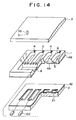
- Fig. 14 shows a partly-broken exploded perspective view of the ink jet head of the fifth embodiment of the present invention.
- the ink jet head of the fifth embodiment has a structure basically identical with that of the third embodiment shown in Fig. 7 and has a characteristic of thin membrane or film for restricting the distance of the gap formed between the vibrating plate 5 and the electrode 21 when the first substrate 1 and the second substrate 2 are combined is made of boro-silicated glass thin membrane 49 and formed on the bottom face of the first substate 1.
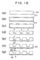
- Fig. 5 shows the manufacturing steps of the first substrate according to the fifth embodiment of the present invention.
- both the faces of silicon wafer of (100) face direction is micro-polished to manufacture a silicon substrate 54 of a thickness 200 ⁇ m (see Fig. 15(d)), and the silicon substrate 54 is thermally oxidization-treated in an oxygen and steam atmosphere at 1100°C, for 4 hours in order to form SiO2 membranes 41a and 41b of thickness 1 ⁇ m on the silicon substrate 54 (see Fig. 15(b)).
- a photo-resist pattern (not shown) corresponding to the shapes of nozzle holes 4, emitting chambers 6, etc. is formed on the upper SiO2 membrane 41a, and the exposed portion of the SiO2 membrane 41a is etched by fluoric acid etching agent in order to remove the photo-resist pattern (see Fig. 15(c)).
- An arisotrophy etching is carried out on the silicon by using alkali agent.
- the nozzle holes 4 and the emitting chamber 6, etc. are formed and then the SiO2 membranes 41a and 42b of anti-etching material are removed by fluoric acid etching magnet (see Fig. 15(d)).
- boro-silicated glass thin membrane 49 functioning as a gap spacer precisely restricting the distance between the vibrating plate 5 and the electrode 21 and as a combined layer attached by an anode bonding method is formed on the lower face of the silicon substrate 54.
- a photo-resist pattern 50 corresponding to a shape of the vibrating plate 5 is formed on the bottom face of the silicon substrate 54 (see Fig. 15(e)).
- a spattering apparatus forms a boro-silicated glass thin membrane 49 on the bottom face of the silicon substrate 54 (see Fig. 15(f)), the silicon substrate 54 is sintered in organic solvent, is added with ultrasound vibration in order to remove the photo-resist pattern 50. Consequently, a boro-silicated glass thin membrane 49 of a gap spacer is formed on the portions or places other than that of the vibrating plate 5 as shown in Fig. 15 (g).
- Corning corporation made #7740 glass is used as a spattering target, a spattering atmosphere is 80% Ar - 20% O2 pressure 5m Torr, and RF power 6W/cm2 is impressed. Thus, 0.5 ⁇ m thickness glass thin membrane 49 is obtained.
- the second substrate 2 and the third substrate 3 shown in Fig. 14 and used to assemble the ink jet head of the present invention are manufactured by the method of the third embodiment.
- the first substrate 1 and third substrate 3 are anode bonding or attached integrally by the method of the third embodiment.
- the vibrating plate 5 formed on the substrate 1 and the electrode 21 formed on the substrate 2 are matched in their positions and they are abutted.
- Combined substrates 1 and 2 are heated to 300°C on a hot plate, a DC voltage 50V is impressed to them for 10 minutes with the first substrate being plus charged and the second substrate being minus charged.
- the ink jet head manufactured according to the fifth embodiment of the present invention is tested in real-printing function and a good result of printing similar to that of the third embodiment is obtained.
- a boro-silicated glass thin membrane 49 is formed on the bottom face of the first substrate 1. It is possible to form the boro-silicated glass thin membrane 49 on the upper face of the second substrate 2 instead of the bottom face of the first substrate 1 obtaining the same effect.
- the boro-silicated glass thin membrane is formed by the method of the fifth embodiment on the second substrate 2.
- a DC voltage 50V is impressed to them with the first substrate being charged plus electricity and the second substrate being charged minus electricity at a temperature 300°C obtaining the ink jet head of a quality and a performance identical with that of the fifth embodiment.
- the fifth embodiment it is possible to bond the first substrate and the second substrate at 300°C obtaining the effects mentioned below.
- Fig. 16 shows a partly-broken perspective view of the first substrate 1 used to the ink jet head according to the sixth embodiment of the present invention.
- the second substrate and the third substrate having electrodes formed thereon of the ink jet head of the sixth embodiment have the structures identical with that of the third embodiment.
- the first substrate 1 of the sixth embodiment is made of the silicon substrate 57 having a p-type silicon substrate 55 and a n-type Si layer 56 epitaxially grown on the bottom face of the p-type silicon substrate 55.
- a part of the p-type silicon substrate 55 is selectively etched through an electric-chemical alkali arisotrophy etching process (be explained later) in order to remove the part obtaining a vibrating plate 5 of a precised thickness.
- the manufacturing steps of the first substrate of the sixth embodiment is shown in Fig. 17.
- both the faces of a silicon wafer of p-type (100) face direction are mirror-polished in order to manufacture a silicon substrate 55 of a thickness 170 ⁇ m, and n-type Si layer 56 of a thickness 30 ⁇ m is epitaxially grown on a bottom face of the silicon substrate 55 obtaining a silicon substrate 57 (see Fig. 17(a)).
- boron is doped into the silicon substrate 55 and its density is 4 x 1015 cm ⁇ 3.
- Al is doped into the n-type Si layer 56 and its density is 5 x 1015 cm ⁇ 3.
- the epitaxial growth process above can form a Si layer 56 having a uniform thickness. It is possible to control the thickness with allowance ⁇ 0.2 ⁇ m of its target of 30 ⁇ m.
- the silicon substrate 57 is brought under heat-oxidization-treatment in an oxygen-steam atmosphere at 1100°C, for 4 hours and SiO2 membranes 41a and 41b of thickness 1 ⁇ m are formed on both the faces of the silicon substrate 57 (see Fig. 17(b)).
- a photo-resist pattern (not shown) corresponding to the shapes of nozzle holes 4, emitting chambers 6, and etc. is formed on the upper SiO2 membrane 41a, a photo-resist pattern (not shown) corresponding to an electrically-led opening portion 58 is formed on the lower SiO2 membrane 41b, then the exposed portions of the SiO2 membranes 41a and 41b are etched by fluoric acid etching agent in order to remove the photo-resist pattern (see Fig. 17(c)).
- a DC voltage of 0.6V is impressed when n-type Si layer 56 is charged plus and platinum plate 80 is charged minus, the silicon substrate 57 is sunk in KOH solution (70°C) containing isopropyl alcohol carrying out an etching step.
- KOH solution 70°C
- n-type Si layer 56 is non-activated by a plus DC voltage preventing the etching process from proceeding. At this time, the etching is finished and the silicon substrate of a condition shown in Fig. 17(d) is obtained.
- a photo-resist (not shown) of a shape corresponding to the vibrating plate 5 is formed on the lower SiO2 membrane 41b, an exposed portion of the SiO2 membrane 41b is etched by fluoric acid etching agent and the photo-resist is removed. Simultaneously, all material of the SiO2 membrane 41a remained on the surface of p-type silicon substrate 55 and the first substrate 1 shown in Fig. 16 is obtained (see Fig. 17(e)).
- the thickness of the vibrating plates of one hundred (100) ink jet head manufacturing by the steps of the sixth embodiment are distributed in a range of 30.0 ⁇ 0.2 ⁇ m and it is the thickness precision of n-type Si layer 56 formed by the epitaxial process.
- the ink jet head of the sixth embodiment is driven with 100V, 5 KHz, the emitting speeds of ink drops are distributed in a range of 8 ⁇ 0.2 ⁇ m/sec. and the ink drop volumes are in a range of (0.1 ⁇ 0.005) x 10 ⁇ 6 cc, resulting in a good printing.
- Fig. 19 shows a partly-broken perspective view of the first substrate used in the ink jet head according to the seventh embodiment of the present invention.
- the second substrate and the third substrate on which electrodes are formed on the ink jet head of the seventh embodiment and the manufacturing method of these substrates are identical with that of the third embodiment, so that explanations for them are omitted from the specification.
- the first substrate 1 of the seventh embodiment is obtained by treating a silicon substrate 63 formed by an epitaxially growing of n-type Si layer 62 on the bottom face of the p-type silicon substrate 61.
- a crystal face direction of p-type silicon substrate 61 is (110).
- the silicon substrate of (110) face direction as well known the (111) face perpendicularly crosses to the substrate face of (110) face direction in a direction (211) and an alkali arisotrophy etching process enables to form a wall structure perpendicularly to the substrate face.
- the seventh embodiment uses the fact above, and pitch distances, when a number of ink jet structural units consisting of nozzles and emitting chambers, etc. are employed, are narrowed realizing a high density arrangement of the nozzles.
- the manufacturing steps of the first substrate of the seventh embodiment is shown in Fig. 20.
- Fig. 20(a) to (d) correspond to that of the C-C line sections of Fig. 19 and steps of Fig. 20 (e) to (g) correspond to the D-D line sections of Fig. 19.
- both the faces of the silicon wafer of p-type (110) face direction are mirror-polished to form a silicon substrate 61 of a thickness 170 ⁇ m
- n-type Si layer 62 of 3 ⁇ m is formed on the bottom face of the silicon substrate 61 by an epitaxial grown step
- the silicon substrate 63 is obtained (see Fig. 20(a)).
- the silicon substrate 61 is doped with B (boron) and its density is 4 x 1015cm ⁇ 3
- the n-type Si layer 62 is doped with A and its density is 5 x 1014 cm ⁇ 3.
- the epitaxial grown step it is possible to control the target thickness 3 ⁇ m within the allowance ⁇ 0.05 ⁇ m.
- the silicon substrate 63 is thermally oxidized-treated at 1100°C in an oxygen and steam atmosphere in order to form SiO2 membranes 41a and 41b of the thickness 1 ⁇ m on both the faces of the silicon substrate 63 (see Fig. 20(b)).
- a photo-resist pattern (not shown) corresponding to the shapes of cavities and ink cavity, etc. is formed on the upper SiO2 membrane 41a, a photo-resist pattern (not shown) corresponding to an electrically leading opening portion 64 is formed on the lower SiO2 membrane 41b, and the exposed portions of the SiO2 membranes 41a and 41b are etched by fluoric acid etching agent to remove the photo-resist pattern (see Fig. 20(c)).
- the size of the photo-resist patterns corresponding to the shape of the emitting chamber 6 its width is 50 ⁇ m, a distance from the neighboring pattern is 20.7 ⁇ m, that is 70.7 ⁇ m of a pitch distance, ink drop density per an inch is 360 dpi (dot per inch).
- the electric-chemical arisotrophy etching mentioned above is applied to the silicon substrate 63 through the method identical with that of the sixth embodiment and the etching is done until the p-type silicon substrate 61 is broken through (see Fig. 20(d)).
- the dents formed in the step shown in Fig. 20(d) consist of perpendicular walls relative to the surfaces of the silicon substrate 63.
- the electric-chemical arisotrophy etching process forms a photo-resist pattern (not shown) corresponding to the nozzles 4 and the orifices 7 on the SiO2 membrane 41a which is a little thinned, a photo-resist membrane (not shown) covers all the lower SiO2 membrane 41b, fluoric acid etching agent etches the exposed portion of the SiO2 membrane 41a, and the photo-resist pattern is removed (see Fig. 20(e)).
- an electric-chemical etching process etches the substrate until the nozzles 4 and the orifices 7 of thickness 30 ⁇ m are formed (see Fig. 20(f)).
- the whole silicon substrate is sunk in fluoric acid etching agent to remove SiO2 membranes 41a and 41b in order to obtain the first substrate 1 (see Fig. 20(g)).
- the width of the emitting chamber formed on the resulting first substrate becomes 55 ⁇ m which is a little enlarged by undercutting during the etching step.
- the pitch distance is 70.7 ⁇ m, so it is said the first substrate obtained has the ideal measurements.
- the most suitable value of the width of the cavity is determined due to ink emitting characteristic. Considering the undercutting, the size of the photo-resist pattern is determined to obtain the ideally-shaped cavity.
- Fig. 21 is a partly-broken perspective view of the first substrate of the ink jet head according to the eighth embodiment of the present invention.
- the vibrating plate 5 in the ink jet head of the eight embodiment of the present invention is a boron doped layer 66 of a density and has a thickness identical with that of the necessay vibrating plate. It is known that the etching rate of alkali used Si etching step becomes very small in the range of a high density (about 5 x 1019 cm ⁇ 3 and more) when the dopant is boron.
- the vibrating plate forming range is supposed that a high density boron doped layer.
- etching stop technique in which the etching rate greatly lessens at the time the boron doped layer 66 is exposed forms of the vibrating plate 5 and emitting chambers 6 of the necessary shapes.
- the faces of a silicon wafer of n-type (110) face direction are mirror-polished in order to form a silicon substrate 65 of a thickness 200 ⁇ m.
- the silicon substrate 65 is brought under a thermal-oxidization treatment of 1100°C for 4 hours in an oxygen and steam atmosphere so as to form SiO2 membranes 41a and 41b of thickness 1 ⁇ m on both the faces of the silicon substrate 65 (see Fig. 22(a)).
- a photo-resist pattern (not shown) corresponding to the shapes of the vibrating plate (boron doped layer) 66, ink cavity 8, electrode leads (not shown) is formed on the lower SiO2 membrane 41b, the exposed portion (part corresponding to the vibrating plate, ink cavity, leads) of the SiO2 membrane 41b is etched by fluoric acid etching agent, and the photo-resist pattern is removed (see Fig. 22 (b)).
- the exposed Si portion of the silicon substrate 65 is doped with boron.
- the treatment method of doping is identical with that of the third embodiment and the boron doping layer 66 of a boron density 5 x 1020 cm ⁇ 3 and of a doped layer thickness 10 ⁇ m is formed (see Fig. 22(c).
- the boron doping layer 66 of a boron density 5 x 1020 cm ⁇ 3 and of a doped layer thickness 10 ⁇ m is formed (see Fig. 22(c).
- a photo-resist pattern (not shown) corresponding to the shapes of emitting chambers 6, ink cavity 8, and etching end detection pattern 71 is formed on the upper SiO2 membrane 41a, the exposed portions of the SiO2 membrane 41a are etched by fluoric acid etching agent, and the photo-resist pattern is removed (see Fig. 22 (d)).
- the photo-resist pattern corresponding to the emitting chamber 6 has a width 50 ⁇ m and apart-distance from the neighboring pattern 20.7 ⁇ m, which are identical with that of the seventh embodiment.
- the silicon substrate 65 is brought under an alkali arisotrophy etching treatment.
- Etching agent of KOH solution density: 20 weight %, temperature: 80 °C
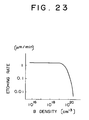
- the etching rates of silicon alkali etching depend on as shown in Fig. 23 the boron density.
- the etching process proceeds at an etching rate of about 1.5 ⁇ m/min, however in the boron high density range the etching rate lowers to about 0.01 ⁇ m/min.
- the thickness (designed value) of the vibrating plate 5 is 10 ⁇ m, it is sufficient to etch and remove only 190 ⁇ m of the total thickness 200 ⁇ m of the silicon substrate 65 in order to form the emitting chambers 6 and the ink cavity 8. In practice, it is difficult to make the thickness of the vibrating plates 5 uniform since the thickness values of the silicon substrates 65 distribute in some range (+ 1 to 2 ⁇ m).
- the process mentioned below can form the thickness to the vibrating plates correctly.
- the etching rate suddenly drops to about 0.01 ⁇ m/min, consequently only about 6 min at most of the etching time length cannot etch the boron doped layer 66 obtaining the vibrating plate having a boron doped layer of thickness 10 ⁇ m.
- the etching step advances at an etching rate of about 1.5 ⁇ m/min.
- a through hole 72 is formed.
- the etching time necessary to make the through hole is distributed owing to various thicknesses of the silicon substrate 65, so it is necessary to detect when the through hole 72 is completed at the time of about 133 min being elapsed after the etching starts through various means (for example, seeing observation of the operator, applying a laser beam on the etching end detection pattern from a side of the pattern and receiving the laser beam by a light receiving element placed on another side of the pattern when the through hole is completed) (see Fig. 22(e)).
- the vibrating plate 5 formed by the process has a precision of 10 ⁇ 0.1 ⁇ m. Such error or allowance of ⁇ 0.1 ⁇ m seems that it depends on distribution of the boron doping depth, and does not depend on the distribution of the alkali etching results.
- the precision of the thickness of boron doped layer determines the thickness precision of the vibrating plate.
- other methods can be used to attain the doped thickness precision corresponding to that obtained by the method of BBr diffusion source.
- the doping is done to the leads continuous to the vibrating plate. Because that the driving electrodes having the structure identical with the vibrating plate of the fourth embodiment and corresponding to each vibrating plate of high density boron doped portions are formed, it is possible also to attain an improvement of the driving frequency.
- n-type substrate is used for the silicon substrate, however if p-type substrate is used for the silicon one, it is possible to form the boron doped vibrating plates.
- Fig.24 shows an outline of the ninth embodiment of the anode bonding method according to the present invention. It shows a section of a bonding apparatus used to the method and of the substrates while they are bonding.
- Fig. 25 is a plan view of the bonding apparatus.
- the ninth embodiment shown relates to an anode bonding method for bonding or the first silicon substrate 1 and the second boro-silicated glass substrate 2.
- the bonding apparatus of the ninth embodiment consists of an anode bonding electrode plate 111 to be connected to a plus side of a power source 113, an cathode bonding electrode plate 112, and a terminal plate 115 protruding from the anode bonding electrode plate 111 through a spring 114.
- Gold plating is applied on the surfaces of the anode bonding electrode plate 111 and the cathode bonding electrode plate 112 in order to decrease contact resistance of the surfaces.
- the terminal plate 115 is constructed by a single contact plate in order to equalize in potential a plurality of electrodes 21 on the boro-silicated glass substrate 2, and the silicon substrate 1.
- the terminal plate 115 is connected to the anode bonding electrode plate 111 by mens of the spring 114 and the spring keeps the terminal plate 115 in its suitable contact pressure with the electrode 21.
- the terminal plate 115 comes to contact with the terminal portion 23 of the electrode 21.
- the silicon substrate 1 and the boro-silicated glass substrate 2 are aligned and in detail the vibrating plate 5 and the electrode 21, respectively formed thereon are aligned by an aligner device (not shown) after they are washed and then they are set as shown in Fig. 24 and Fig. 25.
- the electrode 21, and the electrode plates 111 and 112 are placed in nitrogen gas atmosphere in order to prevent the surfaces of them from being oxidized.
- both the substrates 1 and 2 are heated. In order to prevent the boro-silicated glass substrate 2 from breaking due to sudden rise of temperature, it is necessary to heat it gradually to 300 °C for about 20 min. Next, the power source 113 impresses 500V voltage for about 20 min so as to bond both the substrates 1 and 2.
- the power source 113 impresses 500V voltage for about 20 min so as to bond both the substrates 1 and 2.
- Na ions in the boro-silicated glass substrate 2 move and current flow through the substrate 2. It is possible to judge the joined condition of them when they are connected because a value of current decreases. In order to prevent strain-crack due to thermal conductivities of both the substrates 1 and 2 after they are connected, it is necessary to cool them gradually for about 20 min.
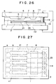
- Fig. 26 is an outline view of another embodiment of the anode bonding method according to the present invention and a section of both the substrates in their bonding procedure and a bonding apparatus used to the anode bonding apparatus.
- Fig.27 is a plan view of the bonding apparatus.
- terminal 116 respectively consisting of coil springs are used and the terminal plates contact with respective electrodes 21.
- Other structure of the embodiment than that above is identical with that shown in Fig. 24.
- the terminals 116 are made of SUS which is durable to high temperature. Ordinarily, a material SUS is not preferable to be used as terminal material because it has resistance on the surface having oxidized films. However, in the anode bonding, it is purpose of applying high voltage and making them equal potential, so that it is possible to obtain good results if a value of current is low.
- respective terminals 16 are independent coil springs, it is possible to prevent the substrates from curving due to being heated when the anode bonding process and these terminals 16 from not being led to the electrode 21 due to worn terminal.
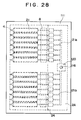
- Fig. 28 shows a plan view of the anode bonding apparatus according to another embodiment of the present invention.
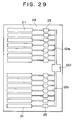
- Fig. 29 is a plan view showing an arrangement relation of the electrode on the second substrate and the common electrode. In Fig. 29, the dielectric membrane is omitted.
- a photolithography uses a batch treatment system in order to form simultaneously a plurality of electrodes 21 for a plural sets (in the embodiment, it is two) of ink jet heads and respectively electrode 21 for the plural sets on a single boro-silicated glass substrate 2A.
- the common electrode 120 has lead portions 121a and 121b to be connected to the terminal portion 23 of all the electrodes 21 of respective sets.
- a single silicon substrate (not shown) to be connected to the boro-silicated glass substrate 2A has a plurality of sets of elements (nozzle, emitting chamber, vibrating plate, orifice, ink cavity) having the structures shown in Fig. 24 and Fig. 26, respective sets being placed at the corresponding positions.
- a single terminal 116 consisting of a coil spring shown in Fig. 26 comes to contact with the common electrode 120 in order to lead it to the anode-side joining electrode plate 111.
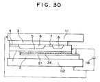
- Fig. 30 is a section of an anode bonding apparatus according to other embodiment of the present invention.
- three substrates 1, 2 and 3 are simultaneously anode-bonding to each other.
- the first substrate 1 is a silicon one
- the second and third substrate 2 and 3 are boro-silicated ones.
- the third substrate 3 function merely as a lid of nozzle holes 4, emitting chamber 6, orifice 7, ink cavity 8. It is enough to make the third substrate 3 of a material of less joining precision than that of boro-silicated glass substrate, so that soda glass joining is sufficient.
- the third substrate is made of boro-silicated glass, it is possible to improve its reliability.
- upper and lower joining electrode plates 111 and 112 to be contacted with the second and third boro-silicated glass substrates 2 and 3 are connected to a minus side of the power source 113, the first silicon substrate 1 and the electrode 21 on the boro-silicated glass substrate 2 are connected to a plus or positive of the power source 113, and they are simultaneously anode bonding.
- the simultaneous anode bonding process it is possible to reduce the time used to heat and gradual cool the substrates 1, 2 and 3 shortening largely the bonding time of them.
- Fig. 31 is a section of a static electricity actuator of the thirteenth embodiment of the present invention.
- Fig. 32 is its plan view.
- the first substrate 1 and the second substrate 2 are directly Si bonding or anode bonding with the predetermined gap length. Because a temperature when the anode bonding or bonding process is done is high, air in the gap portion 16 expands. When air temperature lowers to the room temperature after the connection, the pressure in the gap portion 16 lowers than the atmosphere, so the vibrating plate 5 bends toward the electrode 21 becoming into contact with the electrode 21 and being short-circuited, or more disadvantageously unnecessary stress being given to the vibrating plate 5. When the gap portion 16 is open to the atmosphere in order to prevent such disadvantageous effects and kept at such open condition, static electricity in the gap portion and the surrounding mechanism sucks dust. As a result, such dust is attached to the electrode 21 changing a vibration characteristic of the vibrating plate 5.
- the gap portion 16 of the ink jet head of the thirteenth embodiment of the present invention is open to the atmosphere through the passage 18, as well as outlet ports 19a and 19b of the passage 18 are sealed by sealer agent 20 of epoxy and the like which has a high viscosity when the substrates 1 and 2 are cooled to the room temperature after they are anode-bonding.
- the reference numerals 23 is a terminal portion of the electrode 23, 41 means SiO2 membrane of a dielectric membrane formed on the substrate 1, 102 is an oscillation circuit, and 106 is a metal membrane formed to connect one terminal of the oscillation circuit 102 to the substrate 1.
- the passage 18 extends surround the electrode 21.
- the sealer is made of thermal plastic resin and the pressure in the gap portion does not rise. Because that the sealing member 20 has a high viscosity, it fails to flow-in the passage 18.
- the gap portion 16 is open or led to the atmosphere through the passage 18 while an anode bonding, so that any heating of the anode-bonding operation fails to raise the pressure in the gap portion 16.
- the sealing member 20 seals the outlet of the passage 18 preventing dust from invading the gap portion 16 and the problems above happening.
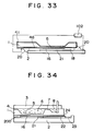
- Fig. 33 is a section of the static electricity actuator according to another embodiment of the present invention.
- the static electricity actuator has a second electrode 46 placed under the vibrating plate 5 so as to oppose to the electrode 21.
- the second electrode 46 is made of Cr or Au thin membrane.
- the static electricity actuator functions as a capacitor.
- Vc V (1 - exp (-t/T) charging time
- Vc V exp (-t/T) discharging time
- T time constant.
- Fig. 34 shows a section of the ink jet head according to still another embodiment of the present invention.
- the gap G to be formed under the vibrating plate 5 is kept by a thickness of photo-sensitive resin layer or adhesive agent layer 200. That is, patterns of the photo-sesitive resin layer or adhesive agent layer 200 are are printed around the electrode 21 of the second substrate 2 and both the second substrate 2 and the first substrate 1 are adhered to each other making a lamination.
- soda glass is used as the second substrate 2 and it is constructed as described on the second embodiment.
- a photo-sensitive polyimid is used as a photo-sensitive resin and it is printed around the electrode 21 of the second substrate 2 with its thickness/ ⁇ m forming the pattern 200 of photo-sensitive resin layer. While, similar to that of the second embodiment, the bottom face of the first silicon substrate 1 is planely polished and the first substrate 1 and second substrate 2 are laminated. As a result, when the photo-sensitive resin is used, the gap length G between the vibrating plate 5 and the electrode 21 is 1.4 ⁇ m. When an adhesive agent of epoxy bond is used, the its thickness G is 1.5 ⁇ m, and the substrates 1 and 2 are laminated at a temperature 100°C. In this case, the gap length G is a little less than 1.9 ⁇ m. When adhesive agent is used, it is necessary to press the substrate 1 and other substrate 2, so the gap length G decreases differing from that of the photo-sensitive resin.
- the ink jet head of the present invention using such gap holding mean scan be driven by a low voltage identical with that of the second embodiment attaining a good printing result.
- thermo-sensitive resin such as acryl, epoxy and the like
- Temperature of thermal treatment is controlled according to the kind of various resins.
- adhesive agents acryl, cyano, urethane, silicon of various materials can be used.
Landscapes
- Engineering & Computer Science (AREA)
- Manufacturing & Machinery (AREA)
- Particle Formation And Scattering Control In Inkjet Printers (AREA)
Applications Claiming Priority (12)
| Application Number | Priority Date | Filing Date | Title |
|---|---|---|---|
| JP145764/92 | 1992-06-05 | ||
| JP14576492 | 1992-06-05 | ||
| JP14576492 | 1992-06-05 | ||
| JP153808/92 | 1992-06-12 | ||
| JP15380892 | 1992-06-12 | ||
| JP15380892 | 1992-06-12 | ||
| JP18123392 | 1992-07-08 | ||
| JP18124092 | 1992-07-08 | ||
| JP181233/92 | 1992-07-08 | ||
| JP181240/92 | 1992-07-08 | ||
| JP18124092 | 1992-07-08 | ||
| JP18123392 | 1992-07-08 |
Publications (3)
| Publication Number | Publication Date |
|---|---|
| EP0580283A2 true EP0580283A2 (de) | 1994-01-26 |
| EP0580283A3 EP0580283A3 (en) | 1995-08-23 |
| EP0580283B1 EP0580283B1 (de) | 1999-09-01 |
Family
ID=27472661
Family Applications (1)
| Application Number | Title | Priority Date | Filing Date |
|---|---|---|---|
| EP93304334A Expired - Lifetime EP0580283B1 (de) | 1992-06-05 | 1993-06-03 | Farbstrahlkopf und sein Herstellungsverfahren |
Country Status (3)
| Country | Link |
|---|---|
| EP (1) | EP0580283B1 (de) |
| JP (4) | JPH0671882A (de) |
| DE (1) | DE69326204T2 (de) |
Cited By (16)
| Publication number | Priority date | Publication date | Assignee | Title |
|---|---|---|---|---|
| EP0609080A3 (de) * | 1993-01-27 | 1995-05-17 | Brother Ind Ltd | Farbstrahlgerät. |
| EP0671372A3 (de) * | 1994-03-09 | 1996-07-10 | Seiko Epson Corp | Anodisches Bindeverfahren und Verfahren zur Herstellung eines Tintenstrahlkopfes unter Verwendung des Bindeverfahrens. |
| EP0707967A3 (de) * | 1994-10-06 | 1997-02-19 | Hewlett Packard Co | Druckkopf |
| EP0867289A1 (de) * | 1994-04-20 | 1998-09-30 | Seiko Epson Corporation | Tintenstrahlaufzeichnungsgerät |
| EP0849082A3 (de) * | 1996-12-20 | 1999-04-14 | Seiko Epson Corporation | Elektrostatischer Betätiger und Verfahren zur Herstellung |
| EP0863007A3 (de) * | 1997-03-03 | 1999-07-07 | Seiko Epson Corporation | Tintenstrahlaufzeichnungskopf |
| US5972086A (en) * | 1995-08-28 | 1999-10-26 | Seiko Epson Corporation | Ink jet printer and ink for ink jet recording |
| EP0888888A3 (de) * | 1997-06-05 | 2000-03-22 | Xerox Corporation | Magnetisch betätigte Tintenstrahldruckvorrichtung |
| US6164759A (en) * | 1990-09-21 | 2000-12-26 | Seiko Epson Corporation | Method for producing an electrostatic actuator and an inkjet head using it |
| US6315394B1 (en) | 1998-01-28 | 2001-11-13 | Seiko Epson Corporation | Method of manufacturing a silicon substrate with a recess, an ink jet head manufacturing method, a silicon substrate with a recess, and an ink jet head |
| US6371598B1 (en) | 1994-04-20 | 2002-04-16 | Seiko Epson Corporation | Ink jet recording apparatus, and an ink jet head |
| US6517195B1 (en) | 1997-04-18 | 2003-02-11 | Seiko Epson Corporation | Ink jet head with an integrated charging control circuit |
| EP1712363A3 (de) * | 2005-04-15 | 2007-12-12 | Seiko Epson Corporation | Elektrostatischer Betätiger für Flüssigkeitsstrahlköpfe |
| WO2007113554A3 (en) * | 2006-04-03 | 2008-02-28 | Xaar Technology Ltd | Droplet deposition apparatus |
| US8317913B2 (en) | 2007-08-14 | 2012-11-27 | Ricoh Company, Ltd. | Inkjet ink, and ink cartridge, inkjet recording method, inkjet recording apparatus and ink record using the same |
| WO2018022036A1 (en) * | 2016-07-27 | 2018-02-01 | Hewlett-Packard Development Company, L.P. | Vibrating a dispense head to move fluid |
Families Citing this family (60)
| Publication number | Priority date | Publication date | Assignee | Title |
|---|---|---|---|---|
| EP0933213B1 (de) * | 1995-04-20 | 2002-07-24 | Seiko Epson Corporation | Tintenstrahldruckvorrichtung und Verfahren zur Steuerung derselben |
| US6000785A (en) * | 1995-04-20 | 1999-12-14 | Seiko Epson Corporation | Ink jet head, a printing apparatus using the ink jet head, and a control method therefor |
| JP3404750B2 (ja) | 1997-03-26 | 2003-05-12 | セイコーエプソン株式会社 | インクジェットヘッド及びその製造方法並びにインクジェット記録装置 |
| JPH11320873A (ja) | 1997-06-05 | 1999-11-24 | Ricoh Co Ltd | インクジェットヘッド |
| US6425656B1 (en) | 1998-01-09 | 2002-07-30 | Seiko Epson Corporation | Ink-jet head, method of manufacture thereof, and ink-jet printer |
| JP2000015804A (ja) | 1998-06-30 | 2000-01-18 | Ricoh Co Ltd | インクジェットヘッド及びその製造方法 |
| JP3628182B2 (ja) | 1998-08-04 | 2005-03-09 | 株式会社リコー | インクジェットヘッド及びその作成方法 |
| JP2000094696A (ja) | 1998-09-24 | 2000-04-04 | Ricoh Co Ltd | インクジェットヘッド及びその作製方法 |
| US6367914B1 (en) | 1999-04-15 | 2002-04-09 | Ricoh Company, Ltd. | Electrostatic ink-jet head and method of production of the same |
| JP2001026105A (ja) | 1999-07-15 | 2001-01-30 | Ricoh Co Ltd | インクジェットヘッド |
| US6485126B1 (en) | 1999-08-05 | 2002-11-26 | Ricoh Company, Ltd. | Ink jet head and method of producing the same |
| JP2001113701A (ja) | 1999-08-06 | 2001-04-24 | Ricoh Co Ltd | 静電型インクジェットヘッドおよびその製造方法 |
| KR100368929B1 (ko) * | 2000-02-01 | 2003-01-24 | 한국과학기술원 | 발열장치 제조방법 및 열분사방식 잉크젯 프린트헤드제조방법 |
| JP2001270110A (ja) | 2000-03-24 | 2001-10-02 | Ricoh Co Ltd | 液滴吐出ヘッド及びインクジェット記録装置 |
| JP4144810B2 (ja) | 2000-06-21 | 2008-09-03 | 株式会社リコー | 液滴吐出ヘッド及びその製造方法、インクジェット記録装置並びに画像形成装置、液滴吐出装置 |
| JP4342749B2 (ja) | 2000-08-04 | 2009-10-14 | 株式会社リコー | 液滴吐出ヘッド、インクカートリッジ及びインクジェット記録装置 |
| US6568794B2 (en) | 2000-08-30 | 2003-05-27 | Ricoh Company, Ltd. | Ink-jet head, method of producing the same, and ink-jet printing system including the same |
| US6299291B1 (en) * | 2000-09-29 | 2001-10-09 | Illinois Tool Works Inc. | Electrostatically switched ink jet device and method of operating the same |
| JP2002248765A (ja) | 2000-12-19 | 2002-09-03 | Fuji Xerox Co Ltd | インクジェット式記録ヘッドおよびインクジェット式記録装置 |
| JP2003001817A (ja) | 2001-06-20 | 2003-01-08 | Ricoh Co Ltd | ヘッド駆動装置及び画像記録装置 |
| US7249816B2 (en) | 2001-09-20 | 2007-07-31 | Ricoh Company, Ltd. | Image recording apparatus and head driving control apparatus |
| EP1506092A4 (de) | 2002-05-20 | 2007-05-09 | Ricoh Kk | Elektrostatisches stellglied und flüssigkeitstropfenausstosskopf mit stabilen betriebseigenschaften gegen umgebungsveränderungen |
| JP4408608B2 (ja) | 2002-06-24 | 2010-02-03 | 株式会社リコー | ヘッド駆動制御装置及び画像記録装置 |
| JP2004042576A (ja) | 2002-07-16 | 2004-02-12 | Ricoh Co Ltd | ヘッド駆動制御装置及び画像記録装置 |
| DE60326962D1 (de) | 2002-08-06 | 2009-05-14 | Ricoh Kk | Durch ein halbleiterherstellungsverfahren gebildetes elektrostatisches stellglied |
| JP4635580B2 (ja) * | 2004-11-25 | 2011-02-23 | セイコーエプソン株式会社 | エッチング液及びその製造方法、並びに液体噴射ヘッドの製造方法 |
| JP4371092B2 (ja) | 2004-12-14 | 2009-11-25 | セイコーエプソン株式会社 | 静電アクチュエータ、液滴吐出ヘッド及びその製造方法、液滴吐出装置並びにデバイス |
| JP4655807B2 (ja) * | 2005-08-02 | 2011-03-23 | セイコーエプソン株式会社 | 静電アクチュエータ、液滴吐出ヘッド及び液滴吐出装置 |
| JP4811067B2 (ja) * | 2006-03-20 | 2011-11-09 | セイコーエプソン株式会社 | 静電アクチュエータ及び液滴吐出ヘッド |
| JP4182360B2 (ja) | 2006-06-05 | 2008-11-19 | セイコーエプソン株式会社 | 液体噴射ヘッド及び液体噴射装置 |
| US8252207B2 (en) | 2006-09-15 | 2012-08-28 | Ricoh Company, Ltd. | Ink for inkjet recording, ink set for inkjet recording, ink media set for inkjet recording, ink cartridge, inkjet recording method, and inkjet recording apparatus |
| JP2009149021A (ja) * | 2007-12-21 | 2009-07-09 | Seiko Epson Corp | 液滴吐出ヘッド、インクジェットプリンタ、液滴吐出ヘッドの製造方法およびインクジェットプリンタの製造方法 |
| JP5381015B2 (ja) | 2008-10-30 | 2014-01-08 | 株式会社リコー | インクジェット記録用インクセット、インクカートリッジ、インクジェット記録方法及びインクジェット記録装置 |
| JP5672065B2 (ja) | 2010-03-02 | 2015-02-18 | 株式会社リコー | インクジェット記録用インク、並びに、インクジェット記録用インクセット、インクカートリッジ、インクジェット記録方法、インクジェット記録装置、及びインク記録物 |
| JP5601075B2 (ja) | 2010-08-04 | 2014-10-08 | 株式会社リコー | インクジェット用インク、並びにインクカートリッジ、インクジェット記録方法、インクジェット記録装置及びインク記録物 |
| JP5825126B2 (ja) | 2011-03-14 | 2015-12-02 | 株式会社リコー | インクジェット用インク、インクジェット記録方法、及びインクジェット記録装置 |
| JP5888589B2 (ja) | 2011-06-28 | 2016-03-22 | 株式会社リコー | インクジェット記録用インク−記録用メディアセット及びインクジェット記録方法 |
| JP5942708B2 (ja) | 2011-09-13 | 2016-06-29 | 株式会社リコー | インクジェット用インク、インクジェット記録方法、インクジェット記録装置及びインク記録物 |
| JP5810883B2 (ja) | 2011-12-14 | 2015-11-11 | 株式会社リコー | 画像形成方法 |
| EP2614964B1 (de) | 2012-01-10 | 2017-01-04 | Ricoh Company, Ltd. | Bilderzeugungsverfahren |
| JP6116864B2 (ja) | 2012-11-12 | 2017-04-19 | 株式会社リコー | 画像形成装置及びその画像形成方法 |
| JP6163797B2 (ja) | 2013-03-06 | 2017-07-19 | 株式会社リコー | 画像形成装置、画像形成システム、画像形成方法及び印刷物の印刷方法 |
| JP6269145B2 (ja) | 2013-03-13 | 2018-01-31 | 株式会社リコー | インクジェット用インク、該インクを用いたインクカートリッジ、インクジェット記録装置、及び、インク記録物 |
| JP6186934B2 (ja) | 2013-06-24 | 2017-08-30 | 株式会社リコー | 液滴吐出ヘッドの制御装置、液滴吐出ヘッド、液滴吐出ヘッドの制御方法及び液滴吐出ヘッドの製造方法、並びに、その制御方法若しくは製造方法のプログラム及びそのプログラムを記録した記録媒体 |
| JP2015034283A (ja) | 2013-07-12 | 2015-02-19 | 株式会社リコー | 水性インクジェット記録用インク、インクジェット記録方法、インクジェット記録物 |
| US9290005B1 (en) | 2014-09-11 | 2016-03-22 | Ricoh Company, Ltd. | Image formation apparatus, method for examining discharge of transparent droplets, and program for examining discharge of transparent droplets |
| JP6696136B2 (ja) | 2014-10-10 | 2020-05-20 | 株式会社リコー | インクセット、及びインクジェット記録方法 |
| JP6645201B2 (ja) | 2015-06-10 | 2020-02-14 | 株式会社リコー | インク、並びにインクジェット記録方法、インクジェット記録装置、及び記録物 |
| US9868288B2 (en) | 2015-07-15 | 2018-01-16 | Ricoh Company, Ltd. | Cleaning liquid for inkjet recording apparatus, method for cleaning inkjet recording apparatus, recording method, and cleaning and filling liquid |
| JP6741230B2 (ja) | 2015-07-27 | 2020-08-19 | 株式会社リコー | インク、インク収容容器及びインクジェット記録装置 |
| US9873252B2 (en) | 2015-12-25 | 2018-01-23 | Ricoh Company, Ltd. | Printing device and printing method |
| JP6696513B2 (ja) | 2016-01-22 | 2020-05-20 | 株式会社リコー | インク、インクと基材のセット、インクジェット印刷方法、インクジェット印刷装置、及び印刷物 |
| US10113078B2 (en) | 2016-10-17 | 2018-10-30 | Ricoh Company, Ltd. | Ink discharge device and ink discharge method |
| CN109863259A (zh) * | 2016-11-03 | 2019-06-07 | Tgo科技株式会社 | 母板、母板的制造方法、掩模的制造方法及oled像素蒸镀方法 |
| WO2019004488A1 (en) | 2017-06-28 | 2019-01-03 | Ricoh Company, Ltd. | INK, INK SET, INK CONTAINER, IMAGE FORMING METHOD, AND IMAGE FORMING APPARATUS |
| EP3540041A1 (de) | 2018-03-16 | 2019-09-18 | Ricoh Company, Ltd. | Verfahren und vorrichtung zur herstellung von zellgewebe |
| EP3686254B1 (de) | 2019-01-25 | 2025-03-12 | Ricoh Company, Ltd. | Tinte, verfahren zur herstellung von tinte, druckverfahren und druckvorrichtung |
| US12270048B2 (en) | 2020-03-23 | 2025-04-08 | Ricoh Company, Ltd. | Manufacturing method for substrate on which nerve cells are arranged |
| JP2023068274A (ja) | 2021-11-02 | 2023-05-17 | 株式会社リコー | 乾燥装置及び画像形成システム |
| JP2024047539A (ja) | 2022-09-26 | 2024-04-05 | 株式会社リコー | インク、画像形成装置、及び画像形成方法 |
Citations (2)
| Publication number | Priority date | Publication date | Assignee | Title |
|---|---|---|---|---|
| JPS6159911A (ja) | 1984-08-30 | 1986-03-27 | Nec Corp | 切換スイツチ回路 |
| EP0479441A2 (de) | 1990-09-21 | 1992-04-08 | Seiko Epson Corporation | Tintenstrahlaufzeichnungsgerät und Verfahren zur Herstellung des Kopfes davon |
Family Cites Families (9)
| Publication number | Priority date | Publication date | Assignee | Title |
|---|---|---|---|---|
| US4312008A (en) * | 1979-11-02 | 1982-01-19 | Dataproducts Corporation | Impulse jet head using etched silicon |
| US4384899A (en) * | 1981-11-09 | 1983-05-24 | Motorola Inc. | Bonding method adaptable for manufacturing capacitive pressure sensing elements |
| GB2146566B (en) * | 1983-09-16 | 1986-11-26 | Standard Telephones Cables Ltd | Electrostatic bonding |
| JPH01246850A (ja) * | 1988-03-29 | 1989-10-02 | Fujitsu Ltd | 半導体基板及びその製法 |
| JPH0212218A (ja) * | 1988-06-30 | 1990-01-17 | Sharp Corp | 可変干渉フィルターの製造方法 |
| JPH02266943A (ja) * | 1989-04-07 | 1990-10-31 | Fujitsu Ltd | インクジェットヘッド |
| JPH03288649A (ja) * | 1990-04-05 | 1991-12-18 | Seiko Epson Corp | 液体噴射ヘッド |
| JPH03295654A (ja) * | 1990-04-13 | 1991-12-26 | Seiko Epson Corp | 液体噴射ヘッド |
| JP2976479B2 (ja) * | 1990-04-17 | 1999-11-10 | セイコーエプソン株式会社 | インクジェットヘッド |
-
1993
- 1993-05-11 JP JP5109654A patent/JPH0671882A/ja active Pending
- 1993-06-03 EP EP93304334A patent/EP0580283B1/de not_active Expired - Lifetime
- 1993-06-03 DE DE69326204T patent/DE69326204T2/de not_active Expired - Lifetime
-
2002
- 2002-02-18 JP JP2002040106A patent/JP3351427B2/ja not_active Expired - Fee Related
- 2002-02-18 JP JP2002040105A patent/JP3381729B2/ja not_active Expired - Fee Related
- 2002-10-17 JP JP2002303235A patent/JP3412628B2/ja not_active Expired - Fee Related
Patent Citations (3)
| Publication number | Priority date | Publication date | Assignee | Title |
|---|---|---|---|---|
| JPS6159911A (ja) | 1984-08-30 | 1986-03-27 | Nec Corp | 切換スイツチ回路 |
| EP0479441A2 (de) | 1990-09-21 | 1992-04-08 | Seiko Epson Corporation | Tintenstrahlaufzeichnungsgerät und Verfahren zur Herstellung des Kopfes davon |
| US5534900A (en) | 1990-09-21 | 1996-07-09 | Seiko Epson Corporation | Ink-jet recording apparatus |
Cited By (30)
| Publication number | Priority date | Publication date | Assignee | Title |
|---|---|---|---|---|
| US6164759A (en) * | 1990-09-21 | 2000-12-26 | Seiko Epson Corporation | Method for producing an electrostatic actuator and an inkjet head using it |
| US6332677B1 (en) | 1992-04-02 | 2001-12-25 | Hewlett-Packard Company | Stable substrate structure for a wide swath nozzle array in a high resolution inkjet printer |
| US5984464A (en) * | 1992-04-02 | 1999-11-16 | Hewlett-Packard Company | Stable substrate structure for a wide swath nozzle array in a high resolution inkjet printer |
| EP0609080A3 (de) * | 1993-01-27 | 1995-05-17 | Brother Ind Ltd | Farbstrahlgerät. |
| US5508726A (en) * | 1993-01-27 | 1996-04-16 | Brother Kogyo Kabushiki Kaisha | Ink jet apparatus |
| EP0861728A3 (de) * | 1993-01-27 | 1998-10-07 | Brother Kogyo Kabushiki Kaisha | Farbstrahlgerät |
| EP0671372A3 (de) * | 1994-03-09 | 1996-07-10 | Seiko Epson Corp | Anodisches Bindeverfahren und Verfahren zur Herstellung eines Tintenstrahlkopfes unter Verwendung des Bindeverfahrens. |
| EP0867289A1 (de) * | 1994-04-20 | 1998-09-30 | Seiko Epson Corporation | Tintenstrahlaufzeichnungsgerät |
| US6371598B1 (en) | 1994-04-20 | 2002-04-16 | Seiko Epson Corporation | Ink jet recording apparatus, and an ink jet head |
| US6213590B1 (en) | 1994-04-20 | 2001-04-10 | Seiko Epson Corporation | Inkjet head for reducing pressure interference between ink supply passages |
| EP0707967A3 (de) * | 1994-10-06 | 1997-02-19 | Hewlett Packard Co | Druckkopf |
| US5972086A (en) * | 1995-08-28 | 1999-10-26 | Seiko Epson Corporation | Ink jet printer and ink for ink jet recording |
| US6176912B1 (en) | 1995-08-28 | 2001-01-23 | Seiko Epson Corporation | Ink jet printer and ink for ink jet recording |
| EP0849082A3 (de) * | 1996-12-20 | 1999-04-14 | Seiko Epson Corporation | Elektrostatischer Betätiger und Verfahren zur Herstellung |
| US6410107B2 (en) | 1996-12-20 | 2002-06-25 | Seiko Epson Corporation | Methods for manufacturing an electrostatic actuator |
| US6190003B1 (en) | 1996-12-20 | 2001-02-20 | Seiko Epson Corporation | Electrostatic actuator and manufacturing method therefor |
| EP0863007A3 (de) * | 1997-03-03 | 1999-07-07 | Seiko Epson Corporation | Tintenstrahlaufzeichnungskopf |
| US6109736A (en) * | 1997-03-03 | 2000-08-29 | Seiko Epson Corporation | Ink jet recording head containing a sealed fluid for protecting a piezoelectric vibrator |
| US6517195B1 (en) | 1997-04-18 | 2003-02-11 | Seiko Epson Corporation | Ink jet head with an integrated charging control circuit |
| US6234608B1 (en) | 1997-06-05 | 2001-05-22 | Xerox Corporation | Magnetically actuated ink jet printing device |
| EP0888888A3 (de) * | 1997-06-05 | 2000-03-22 | Xerox Corporation | Magnetisch betätigte Tintenstrahldruckvorrichtung |
| US6315394B1 (en) | 1998-01-28 | 2001-11-13 | Seiko Epson Corporation | Method of manufacturing a silicon substrate with a recess, an ink jet head manufacturing method, a silicon substrate with a recess, and an ink jet head |
| EP1712363A3 (de) * | 2005-04-15 | 2007-12-12 | Seiko Epson Corporation | Elektrostatischer Betätiger für Flüssigkeitsstrahlköpfe |
| WO2007113554A3 (en) * | 2006-04-03 | 2008-02-28 | Xaar Technology Ltd | Droplet deposition apparatus |
| US8123337B2 (en) | 2006-04-03 | 2012-02-28 | Xaar Technology Limited | Droplet deposition apparatus |
| US8523332B2 (en) | 2006-04-03 | 2013-09-03 | Xaar Technology Limited | Droplet deposition apparatus |
| US8317913B2 (en) | 2007-08-14 | 2012-11-27 | Ricoh Company, Ltd. | Inkjet ink, and ink cartridge, inkjet recording method, inkjet recording apparatus and ink record using the same |
| US8680175B2 (en) | 2007-08-14 | 2014-03-25 | Ricoh Company, Ltd. | Inkjet ink, and ink cartridge, inkjet recording method, inkjet recording apparatus and ink record using the same |
| WO2018022036A1 (en) * | 2016-07-27 | 2018-02-01 | Hewlett-Packard Development Company, L.P. | Vibrating a dispense head to move fluid |
| US11278882B2 (en) | 2016-07-27 | 2022-03-22 | Hewlett-Packard Development Company, L.P. | Vibrating a dispense head to move fluid |
Also Published As
| Publication number | Publication date |
|---|---|
| JP2003118126A (ja) | 2003-04-23 |
| JP3381729B2 (ja) | 2003-03-04 |
| EP0580283B1 (de) | 1999-09-01 |
| JPH0671882A (ja) | 1994-03-15 |
| DE69326204D1 (de) | 1999-10-07 |
| JP2002283569A (ja) | 2002-10-03 |
| EP0580283A3 (en) | 1995-08-23 |
| JP3351427B2 (ja) | 2002-11-25 |
| DE69326204T2 (de) | 2000-03-23 |
| JP2002283579A (ja) | 2002-10-03 |
| JP3412628B2 (ja) | 2003-06-03 |
Similar Documents
| Publication | Publication Date | Title |
|---|---|---|
| EP0580283B1 (de) | Farbstrahlkopf und sein Herstellungsverfahren | |
| US5912684A (en) | Inkjet recording apparatus | |
| EP0479441B1 (de) | Tintenstrahlaufzeichnungsgerät und Verfahren zur Herstellung des Kopfes davon | |
| US6113218A (en) | Ink-jet recording apparatus and method for producing the head thereof | |
| US4639748A (en) | Ink jet printhead with integral ink filter | |
| USRE32572E (en) | Thermal ink jet printhead and process therefor | |
| US4601777A (en) | Thermal ink jet printhead and process therefor | |
| US6164759A (en) | Method for producing an electrostatic actuator and an inkjet head using it | |
| US6168263B1 (en) | Ink jet recording apparatus | |
| JP2000296616A (ja) | インクジェット式記録ヘッド及びインクジェット式記録装置 | |
| JPH10337868A (ja) | 磁気作動インクジェットプリントデバイス及びその製造方法 | |
| KR20100051870A (ko) | 프린트헤드 | |
| US6120124A (en) | Ink jet head having plural electrodes opposing an electrostatically deformable diaphragm | |
| JP2000127379A (ja) | インクジェット式記録ヘッド及びインクジェット式記録装置 | |
| US6371598B1 (en) | Ink jet recording apparatus, and an ink jet head | |
| JPH1134344A (ja) | インクジェットヘッドの製造方法 | |
| KR20070106002A (ko) | 고해상도 잉크젯 프린터 | |
| JP3564864B2 (ja) | インクジェットヘッドの製造方法 | |
| JP4243341B2 (ja) | インクジェットヘッド | |
| JP4055883B2 (ja) | 液滴吐出ヘッド | |
| JPH11165413A (ja) | 静電アクチュエータ | |
| JPH11227195A (ja) | インクジェットヘッド | |
| JPH0469249A (ja) | インクジェットプリンタヘッド | |
| JP2002036550A (ja) | 液滴吐出ヘッド及びその製造方法 | |
| JPH1199647A (ja) | インクジェットヘッド |
Legal Events
| Date | Code | Title | Description |
|---|---|---|---|
| PUAI | Public reference made under article 153(3) epc to a published international application that has entered the european phase |
Free format text: ORIGINAL CODE: 0009012 |
|
| AK | Designated contracting states |
Kind code of ref document: A2 Designated state(s): DE FR GB |
|
| PUAL | Search report despatched |
Free format text: ORIGINAL CODE: 0009013 |
|
| AK | Designated contracting states |
Kind code of ref document: A3 Designated state(s): DE FR GB |
|
| 17P | Request for examination filed |
Effective date: 19960127 |
|
| 17Q | First examination report despatched |
Effective date: 19960221 |
|
| GRAG | Despatch of communication of intention to grant |
Free format text: ORIGINAL CODE: EPIDOS AGRA |
|
| GRAG | Despatch of communication of intention to grant |
Free format text: ORIGINAL CODE: EPIDOS AGRA |
|
| GRAH | Despatch of communication of intention to grant a patent |
Free format text: ORIGINAL CODE: EPIDOS IGRA |
|
| GRAH | Despatch of communication of intention to grant a patent |
Free format text: ORIGINAL CODE: EPIDOS IGRA |
|
| GRAA | (expected) grant |
Free format text: ORIGINAL CODE: 0009210 |
|
| AK | Designated contracting states |
Kind code of ref document: B1 Designated state(s): DE FR GB |
|
| REF | Corresponds to: |
Ref document number: 69326204 Country of ref document: DE Date of ref document: 19991007 |
|
| ET | Fr: translation filed | ||
| PLBE | No opposition filed within time limit |
Free format text: ORIGINAL CODE: 0009261 |
|
| STAA | Information on the status of an ep patent application or granted ep patent |
Free format text: STATUS: NO OPPOSITION FILED WITHIN TIME LIMIT |
|
| 26N | No opposition filed | ||
| REG | Reference to a national code |
Ref country code: GB Ref legal event code: IF02 |
|
| PGFP | Annual fee paid to national office [announced via postgrant information from national office to epo] |
Ref country code: FR Payment date: 20100709 Year of fee payment: 18 |
|
| PGFP | Annual fee paid to national office [announced via postgrant information from national office to epo] |
Ref country code: GB Payment date: 20100602 Year of fee payment: 18 |
|
| PGFP | Annual fee paid to national office [announced via postgrant information from national office to epo] |
Ref country code: DE Payment date: 20110601 Year of fee payment: 19 |
|
| GBPC | Gb: european patent ceased through non-payment of renewal fee |
Effective date: 20110603 |
|
| REG | Reference to a national code |
Ref country code: FR Ref legal event code: ST Effective date: 20120229 |
|
| PG25 | Lapsed in a contracting state [announced via postgrant information from national office to epo] |
Ref country code: FR Free format text: LAPSE BECAUSE OF NON-PAYMENT OF DUE FEES Effective date: 20110630 |
|
| PG25 | Lapsed in a contracting state [announced via postgrant information from national office to epo] |
Ref country code: GB Free format text: LAPSE BECAUSE OF NON-PAYMENT OF DUE FEES Effective date: 20110603 |
|
| REG | Reference to a national code |
Ref country code: DE Ref legal event code: R119 Ref document number: 69326204 Country of ref document: DE Effective date: 20130101 |
|
| PG25 | Lapsed in a contracting state [announced via postgrant information from national office to epo] |
Ref country code: DE Free format text: LAPSE BECAUSE OF NON-PAYMENT OF DUE FEES Effective date: 20130101 |