EP0583038A1 - Circuit d'alimentation et circuit de commande destiné à être utilisé dans un circuit d'alimentation - Google Patents
Circuit d'alimentation et circuit de commande destiné à être utilisé dans un circuit d'alimentation Download PDFInfo
- Publication number
- EP0583038A1 EP0583038A1 EP93202345A EP93202345A EP0583038A1 EP 0583038 A1 EP0583038 A1 EP 0583038A1 EP 93202345 A EP93202345 A EP 93202345A EP 93202345 A EP93202345 A EP 93202345A EP 0583038 A1 EP0583038 A1 EP 0583038A1
- Authority
- EP
- European Patent Office
- Prior art keywords
- power supply
- supply circuit
- circuit
- signal
- switch
- Prior art date
- Legal status (The legal status is an assumption and is not a legal conclusion. Google has not performed a legal analysis and makes no representation as to the accuracy of the status listed.)
- Withdrawn
Links
Images

Classifications
-
- H—ELECTRICITY
- H02—GENERATION; CONVERSION OR DISTRIBUTION OF ELECTRIC POWER
- H02M—APPARATUS FOR CONVERSION BETWEEN AC AND AC, BETWEEN AC AND DC, OR BETWEEN DC AND DC, AND FOR USE WITH MAINS OR SIMILAR POWER SUPPLY SYSTEMS; CONVERSION OF DC OR AC INPUT POWER INTO SURGE OUTPUT POWER; CONTROL OR REGULATION THEREOF
- H02M3/00—Conversion of DC power input into DC power output
- H02M3/22—Conversion of DC power input into DC power output with intermediate conversion into AC
- H02M3/24—Conversion of DC power input into DC power output with intermediate conversion into AC by static converters
- H02M3/28—Conversion of DC power input into DC power output with intermediate conversion into AC by static converters using discharge tubes with control electrode or semiconductor devices with control electrode to produce the intermediate AC
- H02M3/325—Conversion of DC power input into DC power output with intermediate conversion into AC by static converters using discharge tubes with control electrode or semiconductor devices with control electrode to produce the intermediate AC using devices of a triode or a transistor type requiring continuous application of a control signal
- H02M3/335—Conversion of DC power input into DC power output with intermediate conversion into AC by static converters using discharge tubes with control electrode or semiconductor devices with control electrode to produce the intermediate AC using devices of a triode or a transistor type requiring continuous application of a control signal using semiconductor devices only
- H02M3/33507—Conversion of DC power input into DC power output with intermediate conversion into AC by static converters using discharge tubes with control electrode or semiconductor devices with control electrode to produce the intermediate AC using devices of a triode or a transistor type requiring continuous application of a control signal using semiconductor devices only with automatic control of the output voltage or current, e.g. flyback converters
-
- H—ELECTRICITY
- H02—GENERATION; CONVERSION OR DISTRIBUTION OF ELECTRIC POWER
- H02M—APPARATUS FOR CONVERSION BETWEEN AC AND AC, BETWEEN AC AND DC, OR BETWEEN DC AND DC, AND FOR USE WITH MAINS OR SIMILAR POWER SUPPLY SYSTEMS; CONVERSION OF DC OR AC INPUT POWER INTO SURGE OUTPUT POWER; CONTROL OR REGULATION THEREOF
- H02M3/00—Conversion of DC power input into DC power output
-
- H—ELECTRICITY
- H02—GENERATION; CONVERSION OR DISTRIBUTION OF ELECTRIC POWER
- H02M—APPARATUS FOR CONVERSION BETWEEN AC AND AC, BETWEEN AC AND DC, OR BETWEEN DC AND DC, AND FOR USE WITH MAINS OR SIMILAR POWER SUPPLY SYSTEMS; CONVERSION OF DC OR AC INPUT POWER INTO SURGE OUTPUT POWER; CONTROL OR REGULATION THEREOF
- H02M1/00—Details of apparatus for conversion
- H02M1/0003—Details of control, feedback or regulation circuits
- H02M1/0032—Control circuits allowing low power mode operation, e.g. in standby mode
-
- Y—GENERAL TAGGING OF NEW TECHNOLOGICAL DEVELOPMENTS; GENERAL TAGGING OF CROSS-SECTIONAL TECHNOLOGIES SPANNING OVER SEVERAL SECTIONS OF THE IPC; TECHNICAL SUBJECTS COVERED BY FORMER USPC CROSS-REFERENCE ART COLLECTIONS [XRACs] AND DIGESTS
- Y02—TECHNOLOGIES OR APPLICATIONS FOR MITIGATION OR ADAPTATION AGAINST CLIMATE CHANGE
- Y02B—CLIMATE CHANGE MITIGATION TECHNOLOGIES RELATED TO BUILDINGS, e.g. HOUSING, HOUSE APPLIANCES OR RELATED END-USER APPLICATIONS
- Y02B70/00—Technologies for an efficient end-user side electric power management and consumption
- Y02B70/10—Technologies improving the efficiency by using switched-mode power supplies [SMPS], i.e. efficient power electronics conversion e.g. power factor correction or reduction of losses in power supplies or efficient standby modes
Definitions
- the invention relates to a power supply circuit having input terminals for receiving an input voltage and output terminals for supplying an output voltage, which circuit comprises, coupled parallel to the input terminals of the power supply circuit, a series arrangement of a primary winding of a transformer and a switch, a secondary winding of the transformer coupled to the output terminals of the power supply circuit and a control circuit having an input which is coupled to the output terminals of the power supply circuit and an output for applying a control signal to the switch, said control circuit comprising an oscillator circuit for generating a pulse width-modulated control signal having a predetermined frequency.
- the invention also relates to a control circuit for use in such a power supply circuit.
- a power supply circuit of this type is known from German Patent Specification DE-C-3444035.
- pulse width modulation also referred to as duty cycle control
- PWM pulse width modulation
- a drawback of pulse width modulation is that the width of the pulse has a minimum. If the load decreases, the width of the pulse is reduced so as to keep the output voltage equal. Since the pulse is applied to a control electrode of, for example a transistor operating as a switch, it will take some time at the moment of the start of the pulse before the switch is rendered conducting. Moreover, at the end of the pulse it will take some time before the switch becomes non-conducting. At a given pulse width the switch will be conducting for a given minimum period of time and a further reduction of the pulse width does not have any influence on the conductivity time of the switch, until the width of the pulse becomes so narrow that the switch is not rendered conducting at all anymore.
- Apparatuses such as television receivers, etc. in particular are in a standby mode for the greater part of the time.
- a small part of the apparatus is power supplied, inter alia, for example the reception section of the remote control unit.
- a general object is to ensure that the apparatuses in the standby mode consume a minimum quantity of energy. Due to this object, the width of the pulse in the standby mode becomes increasingly narrower when using pulse width modulation, so that the above-mentioned problems arise, or even get worse. Also in applications in which a (mains-supplied) apparatus requires a small quantity of power during a given part of the time (which need not be the above-mentioned standby mode) the above-mentioned problems occur.
- a further drawback of this known control is that audible transformer noise occurs. This is a vibration of the core (caused, inter alia by the air gap) and of the wires of the windings of the transformer, which vibration occurs in the transformer due to a low-frequency varying magnetic field.
- a power supply circuit is characterized in that the control circuit is adapted to receive a feedback signal at the input of the power to be supplied at the output terminals of the power supply circuit and is adapted to receive at a further input a signal to be externally set, said control circuit also comprising switching means for switching an oscillator of the oscillator circuit from the predetermined frequency to another fixed frequency in dependence upon the signal to be externally set and the feedback signal.
- Switching the frequency when detecting that the load connected to the power supply circuit requires a power which is below the externally set value has the advantage that the duty cycle of the switch maintains such a value that this duty cycle remains above the minimum value.
- the power supply circuit operates more effectively because the losses in the different elements of the power supply circuit relatively become increasingly larger when the power required by the load is supplied, hence at a smaller duty cycle.
- the switch is switched on for longer periods of time in succession, but at a lower frequency.
- the two frequencies of the oscillator circuit may differ, for example by a factor of two.
- An embodiment of a power supply circuit according to the invention is characterized in that the control circuit comprises means for detecting the moment of switching to the other fixed frequency with reference to a current flowing through the switch during operation.
- a further embodiment of a power supply circuit according to the invention is characterized in that the means comprise a differential amplifier for amplifying the difference between the feedback signal and a reference signal, an output of the differential amplifier being coupled to the switching means.
- control circuit comprises means for detecting the moment of switching to the other fixed frequency with reference to the given duty cycle, said means comprising an extra winding on the transformer, and a duty cycle detection circuit for detecting the duty cycle and for supplying a switching signal to the oscillator circuit.
- the control circuit may be an integrated circuit and can also be used in other power supply circuits.
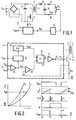
- Fig. 1 shows a power supply circuit V which receives an input alternating voltage Vin (for example, the mains voltage) at input terminals 1 and 2.
- the input terminals are connected to a rectifier 3 for full-wave rectification of the input alternating voltage.
- a buffer capacitor 5 is connected across outputs of the rectifier.
- a series arrangement of a primary winding 7 of a transformer T and a transistor 9 operating as a switch is arranged parallel to this capacitor (in this embodiment the transistor is an NPN transistor, but a FET is alternatively possible; the choice of the type of transistor/switch is determined by specific design requirements and is known to those skilled in the art).
- a secondary winding 11 of the transformer is connected to a series arrangement of a diode 13 and a capacitor 15.
- Output terminals 17 and 18 of the power supply circuit V supply an output voltage Vout across the capacitor 15.
- a load Rb (shown as a resistor) is connected across the output terminals. This load may be, for example all kinds of components of a display device, radio, CD player but also, for example a lamp.
- the power supply circuit V further comprises a detection circuit 19 for detecting the energy to be supplied by the power supply circuit.
- the detection circuit supplies a signal Vfb to a control circuit 21 which, dependent on the load determined by the detection circuit (the power required), controls the period of conductance of the transistor 9.
- the detection circuit may comprise, for example a differential amplifier and an opto-coupler for maintaining a DC separation between the load (Rb) and the input side of the power supply circuit.
- the control circuit 21 also has a second input for receiving a predetermined minimum power Pset (the control circuit 21 will be further described with reference to Figs. 2 and 3).
- such a power supply circuit is used, for example in a display device.
- the majority of present-day display devices uses a standby mode, in which mode the display device is switched off and can be switched on by means of, for example a remote control unit.
- the load is much lower than during normal use (during the standby mode, inter alia the display tube is not provided with the high voltage required for display).
- the control circuit 21 will therefore control the transistor (switch 9) with a much smaller duty cycle (a lower load requires less power).
- the width of the pulse is reduced so as to keep the output voltage equal. Since the pulse is applied to a control electrode of, for example a transistor operating as a switch, it will take some time at the moment when the pulse starts before the switch is rendered conducting (which is caused by the inertia of the transistor). At the end of the pulse it will also take some time before the switch becomes non-conducting. At a given pulse width the switch will be conducting for a given minimum period of time and a further reduction of the pulse width does not have any influence on the conductivity time of the switch, until the width of the pulse becomes so narrow that the switch does not become conducting at all anymore.
- Apparatuses such as television receivers, etc. in particular are in a standby mode for the greater part of the time. During this time only a small part of the apparatus is power supplied, inter alia, for example the reception section of the remote control unit.
- a general object is to ensure that the apparatuses in the standby mode consume a minimum quantity of energy. Due to this object, the width of the pulse in the standby mode becomes increasingly narrower when using pulse width modulation, so that the above-mentioned problems arise, or even get worse.
- a second problem which occurs when the load is derived (for example, during the standby mode) is that the power supply circuit becomes less effective at low loads. This implies that a relatively larger quantity of power is lost (is dissipated in the different elements of the power supply circuit) so that, relatively, an increasingly smaller quantity of power is available for the load.
- Fig. 2a shows a first embodiment of the control circuit 21.
- the control circuit receives the signal Vfb from the detection circuit 19 and applies this signal to a first input of a differential amplifier 23.
- the differential amplifier receives a reference voltage Vref at a second input.
- This reference voltage is a voltage across the outputs 17, 18 (see Fig. 1) of the power supply circuit V (or a part thereof if Vfb via, for example a resistance division is also a part of the output voltage).
- the differential amplifier supplies the amplified difference as a voltage Ver at an output.
- the voltage Ver is applied to an input of a comparator 25.
- a second input of the comparator receives a signal Is which is a measure of the current flowing through the switch 9' (shown in this example as a FET) (measured across a measuring resistor Rm).
- An output of the comparator 25 is connected to a reset input R of a flip-flop 27.
- the flip-flop receives a signal Vosc at a set input S, which signal originates from an oscillator circuit 29.
- Fig. 2c shows the different signals with respect to time.
- the signal Vosc has a (digital) high value.
- an output Q of the flip-flop 27 becomes digitally high, hence the output Q' (NOT-Q) becomes low.
- the output Q' of the flip-flop is connected to an inverting amplifier 31, which amplifier controls the switch 9' via an output resistor 33 having a voltage Vout.
- the current through the switch and through the measuring resistor Rm increases with a sawtooth shape.
- control circuit also comprises a standby circuit 35 which receives the signal Ver at a first input.
- the standby circuit receives a signal Pset at a second input, which signal determines at which power consumption of the load the oscillator circuit 29 must switch. If the power consumption of the load decreases, the output signal Ver of the differential amplifier 23 also decreases.
- the standby circuit 35 determines with reference to the signal Ver (which is thus a measure of the power consumption) and with reference to the signal Pset when the frequency of the oscillator circuit 29 must be switched. The frequency of the oscillator is thus switched at a given minimum power (Pset).
- the power consumption is determined with reference to the signal Ver (which corresponds to a minimum peak current through the switch).
- the frequency of the oscillator circuit is reduced so as to ensure that the switch (9, 9') is uninterruptedly on for a longer time (but at a lower repetition frequency) and to ensure that the power supply circuit is used more effectively.
- the graph for the current Is with Ver-stby shows the value of the output of the differential amplifier 23 at a low power consumption (for example during standby).
- Fh the high frequency
- Fl the low frequency
- Arrows show the variation at a decreasing power consumption of the load.
- the term standby circuit 35 raises the presumption that the apparatus in which this power supply circuit/control circuit is used has a standby mode. However, whether the apparatus has a standby mode is not important for the invention and for this power supply circuit.
- Fig. 3a shows a second embodiment of a control circuit 21 for use in a power supply circuit V (see Fig. 1). Elements having the same reference numerals as in Fig. 1 and/or 2 operate in a similar way.
- control circuit receives the signal Vfb from the detection circuit 19 (see Fig. 1).
- the signal Vfb is applied to an input of the differential amplifier 23 which receives the reference signal Vref at a second input again.
- the differential amplifier again supplies the signal Ver to an input of the comparator 25.
- the comparator receives the signal Is again at a second input (which is measure of the current through the switch 9').
- the output signal of the comparator again serves as a reset signal R for the flip-flop 27.
- the output signal Vosc of the oscillator circuit 29 again serves as a set signal S for the flip-flop.
- the flip-flop also supplies the signal Q' (NOT-Q) to the inverting amplifier 31 whose output again supplies the output signal Vout as a control signal to the switch via the output resistor 33.
- an extra winding 37 on the transformer T is used instead of the signal Ver.
- This extra winding is connected to a duty cycle detection circuit 39 for determining the duty cycle of the switch 9' and for determining the switching moment of the oscillator circuit 29 with reference to the signal Pset.
- the duty cycle detection circuit determines the switching moment with reference to the duty cycle and the input signal Pset. This is shown diagrammatically in Fig. 3b. At a decreasing power (in the direction of the arrows) the duty cycle D reaches the value Dmin at a given moment, which value corresponds to a power consumption of Pset of the load.
- the duty cycle detection circuit 39 then supplies a signal to the oscillator circuit 29 whereupon the frequency of Fh is decreased to Fl (for example halved).
- Fl for example halved
Landscapes
- Engineering & Computer Science (AREA)
- Power Engineering (AREA)
- Dc-Dc Converters (AREA)
- Rectifiers (AREA)
Applications Claiming Priority (2)
| Application Number | Priority Date | Filing Date | Title |
|---|---|---|---|
| NL9201428A NL9201428A (nl) | 1992-08-10 | 1992-08-10 | Voedingsschakeling en stuurschakeling voor toepassing in een voedingsschakeling. |
| NL9201428 | 1992-08-10 |
Publications (1)
| Publication Number | Publication Date |
|---|---|
| EP0583038A1 true EP0583038A1 (fr) | 1994-02-16 |
Family
ID=19861163
Family Applications (1)
| Application Number | Title | Priority Date | Filing Date |
|---|---|---|---|
| EP93202345A Withdrawn EP0583038A1 (fr) | 1992-08-10 | 1993-08-09 | Circuit d'alimentation et circuit de commande destiné à être utilisé dans un circuit d'alimentation |
Country Status (5)
| Country | Link |
|---|---|
| US (1) | US5469349A (fr) |
| EP (1) | EP0583038A1 (fr) |
| JP (1) | JPH06165491A (fr) |
| KR (1) | KR100351214B1 (fr) |
| NL (1) | NL9201428A (fr) |
Cited By (9)
| Publication number | Priority date | Publication date | Assignee | Title |
|---|---|---|---|---|
| WO1995030183A1 (fr) * | 1994-04-29 | 1995-11-09 | Thomas Burger | Circuit electronique permettant de reduire la consommation de courant d'un transformateur |
| EP0709948A1 (fr) * | 1994-10-27 | 1996-05-01 | STMicroelectronics S.r.l. | Convertisseur continu-continu fonctionnant en mode d'élimination d'impulsions sous des conditions de charge faible |
| EP0750389A3 (fr) * | 1995-06-23 | 1997-11-12 | Siemens Aktiengesellschaft | Convertisseur |
| US5745352A (en) * | 1994-10-27 | 1998-04-28 | Sgs-Thomson Microelectronics S.R.L. | DC-to-DC converter functioning in a pulse-skipping mode with low power consumption and PWM inhibit |
| WO2000059103A1 (fr) * | 1999-03-26 | 2000-10-05 | Sarnoff Corporation | Alimentation a faible dissipation de puissance et commande |
| EP1089420A1 (fr) * | 1999-09-02 | 2001-04-04 | Yokogawa Electric Corporation | Alimentation de puissance à découpage |
| WO2002003537A1 (fr) | 2000-06-30 | 2002-01-10 | Power Integrations, Inc. | Procede et appareil |
| FR2819063A1 (fr) * | 2000-12-28 | 2002-07-05 | Ge Fanuc Automation Inc | Procede et circuit pour reduire la dissipation thermique dans un boitier d'automate programmable industriel, et automate programmable industriel integrant un tel circuit |
| WO2005027330A1 (fr) * | 2003-09-13 | 2005-03-24 | Ashraf Said Mohammed Hassan | Generateur electronique |
Families Citing this family (20)
| Publication number | Priority date | Publication date | Assignee | Title |
|---|---|---|---|---|
| DE59404962D1 (de) * | 1994-07-18 | 1998-02-12 | Siemens Ag | Gleichstromumrichter mit Strombegrenzung |
| US5657218A (en) * | 1994-09-07 | 1997-08-12 | Deutsche Thomson Brandt Gmbh | Switch mode power supply circuit |
| DE4436553A1 (de) * | 1994-10-13 | 1996-04-18 | Philips Patentverwaltung | Stromversorgungseinrichtung |
| DE4438671C1 (de) * | 1994-10-28 | 1996-05-15 | Sgs Thomson Microelectronics | Schaltungsanordnung zur Ansteuerung eines Umrichters |
| EP0748027B1 (fr) | 1995-06-07 | 2006-09-06 | General Electric Company | Machine dynamo-électrique et construction de rotor pour celle-ci |
| US6307356B1 (en) * | 1998-06-18 | 2001-10-23 | Linear Technology Corporation | Voltage mode feedback burst mode circuit |
| TW459438B (en) | 1999-09-17 | 2001-10-11 | Koninkl Philips Electronics Nv | Multimode switched-mode power supply |
| US6462971B1 (en) | 1999-09-24 | 2002-10-08 | Power Integrations, Inc. | Method and apparatus providing a multi-function terminal for a power supply controller |
| US6674274B2 (en) | 2001-02-08 | 2004-01-06 | Linear Technology Corporation | Multiple phase switching regulators with stage shedding |
| JP2002247847A (ja) * | 2001-02-20 | 2002-08-30 | Internatl Business Mach Corp <Ibm> | Acアダプタ、電源供給装置、電気機器、および電源供給装置の制御方法 |
| US6480401B2 (en) * | 2001-03-13 | 2002-11-12 | Astec International Limited | Method and apparatus for reducing standby power in power supplies |
| US6611439B1 (en) * | 2002-10-28 | 2003-08-26 | System General Corporation | PWM controller for controlling output power limit of a power supply |
| WO2004054080A1 (fr) * | 2002-12-12 | 2004-06-24 | Sanken Electric Co., Ltd. | Appareil d'alimentation electrique en courant continu |
| KR101020243B1 (ko) | 2004-06-16 | 2011-03-07 | 페어차일드코리아반도체 주식회사 | 스위칭 모드 파워 서플라이 |
| US7358707B2 (en) * | 2005-08-02 | 2008-04-15 | Dell Products L.P. | Information handling system including a power supply unit with a power converter for supplying power to multiple outputs |
| US7696737B2 (en) * | 2007-12-21 | 2010-04-13 | Power Intergrations, Inc. | Method and apparatus to control a power supply for high efficiency |
| KR101468719B1 (ko) * | 2008-03-12 | 2014-12-05 | 페어차일드코리아반도체 주식회사 | 전력 변환기 및 그 구동 방법 |
| DE102010014103A1 (de) | 2010-04-07 | 2011-10-13 | Austriamicrosystems Ag | Frequenzauswahlschaltung für einen Gleichstromwandler und Verfahren zur Auswahl einer Frequenz desselben |
| IT1403601B1 (it) * | 2010-12-22 | 2013-10-31 | St Microelectronics Srl | Dispositivo di controllo di un convertitore dc-dc. |
| CN103760408B (zh) | 2014-01-26 | 2017-02-15 | 矽力杰半导体技术(杭州)有限公司 | 过零检测电路 |
Citations (3)
| Publication number | Priority date | Publication date | Assignee | Title |
|---|---|---|---|---|
| WO1987004885A1 (fr) * | 1986-01-31 | 1987-08-13 | Deutsche Thomson-Brandt Gmbh | Interrupteur de secteur pour appareils de television |
| EP0244623A2 (fr) * | 1986-05-05 | 1987-11-11 | Motorola, Inc. | Circuit de redémarrage automatique pour alimentation de puissance à découpage |
| US4772995A (en) * | 1987-01-08 | 1988-09-20 | Veeco Instruments Inc. | Switching supply with pulse width and rate modulation |
Family Cites Families (2)
| Publication number | Priority date | Publication date | Assignee | Title |
|---|---|---|---|---|
| US4791544A (en) * | 1984-09-21 | 1988-12-13 | Veeco Instruments | Regulating control for single-ended switching power supply |
| DE3444035A1 (de) * | 1984-12-03 | 1986-06-05 | Klöckner-Moeller Elektrizitäts GmbH, 5300 Bonn | Regelprinzip fuer schaltnetzteil |
-
1992
- 1992-08-10 NL NL9201428A patent/NL9201428A/nl not_active Application Discontinuation
-
1993
- 1993-08-06 KR KR1019930015238A patent/KR100351214B1/ko not_active Expired - Fee Related
- 1993-08-09 EP EP93202345A patent/EP0583038A1/fr not_active Withdrawn
- 1993-08-10 US US08/105,212 patent/US5469349A/en not_active Expired - Lifetime
- 1993-08-10 JP JP5198411A patent/JPH06165491A/ja active Pending
Patent Citations (3)
| Publication number | Priority date | Publication date | Assignee | Title |
|---|---|---|---|---|
| WO1987004885A1 (fr) * | 1986-01-31 | 1987-08-13 | Deutsche Thomson-Brandt Gmbh | Interrupteur de secteur pour appareils de television |
| EP0244623A2 (fr) * | 1986-05-05 | 1987-11-11 | Motorola, Inc. | Circuit de redémarrage automatique pour alimentation de puissance à découpage |
| US4772995A (en) * | 1987-01-08 | 1988-09-20 | Veeco Instruments Inc. | Switching supply with pulse width and rate modulation |
Non-Patent Citations (1)
| Title |
|---|
| PATENT ABSTRACTS OF JAPAN vol. 5, no. 15 (E-43)29 January 1981 & JP-A-55 141 973 ( SHINDENGEN ELECTRIC MFG CO ) 6 November 1980 * |
Cited By (16)
| Publication number | Priority date | Publication date | Assignee | Title |
|---|---|---|---|---|
| WO1995030183A1 (fr) * | 1994-04-29 | 1995-11-09 | Thomas Burger | Circuit electronique permettant de reduire la consommation de courant d'un transformateur |
| EP0709948A1 (fr) * | 1994-10-27 | 1996-05-01 | STMicroelectronics S.r.l. | Convertisseur continu-continu fonctionnant en mode d'élimination d'impulsions sous des conditions de charge faible |
| US5745352A (en) * | 1994-10-27 | 1998-04-28 | Sgs-Thomson Microelectronics S.R.L. | DC-to-DC converter functioning in a pulse-skipping mode with low power consumption and PWM inhibit |
| EP0750389A3 (fr) * | 1995-06-23 | 1997-11-12 | Siemens Aktiengesellschaft | Convertisseur |
| WO2000059103A1 (fr) * | 1999-03-26 | 2000-10-05 | Sarnoff Corporation | Alimentation a faible dissipation de puissance et commande |
| US6295217B1 (en) | 1999-03-26 | 2001-09-25 | Sarnoff Corporation | Low power dissipation power supply and controller |
| EP1089420A1 (fr) * | 1999-09-02 | 2001-04-04 | Yokogawa Electric Corporation | Alimentation de puissance à découpage |
| EP2276160A2 (fr) | 2000-06-30 | 2011-01-19 | Power Integrations, Inc. | Procédé et appareil pour l'amélioration du rendement dans un régulateur à découpage près des charges légères. |
| EP1256162A4 (fr) * | 2000-06-30 | 2006-04-12 | Power Integrations Inc | Procede et appareil pour l'amelioration du rendement dans un regulateur a decoupage pres des charges legeres. |
| WO2002003537A1 (fr) | 2000-06-30 | 2002-01-10 | Power Integrations, Inc. | Procede et appareil |
| EP2276161A2 (fr) | 2000-06-30 | 2011-01-19 | Power Integrations, Inc. | Procédé et appareil pour améliorer l'efficacité de commutation de régulateur en charges légères |
| EP2276161A3 (fr) * | 2000-06-30 | 2012-01-25 | Power Integrations, Inc. | Procédé et appareil pour améliorer l'efficacité de commutation de régulateur en charges légères |
| EP2276160A3 (fr) * | 2000-06-30 | 2012-02-22 | Power Integrations, Inc. | Procédé et appareil pour l'amélioration du rendement dans un régulateur à découpage près des charges légères. |
| FR2819063A1 (fr) * | 2000-12-28 | 2002-07-05 | Ge Fanuc Automation Inc | Procede et circuit pour reduire la dissipation thermique dans un boitier d'automate programmable industriel, et automate programmable industriel integrant un tel circuit |
| US6978386B2 (en) | 2000-12-28 | 2005-12-20 | Ge Fanuc Automation North America, Inc. | Method and apparatus for regulating current for programmable logic controllers |
| WO2005027330A1 (fr) * | 2003-09-13 | 2005-03-24 | Ashraf Said Mohammed Hassan | Generateur electronique |
Also Published As
| Publication number | Publication date |
|---|---|
| JPH06165491A (ja) | 1994-06-10 |
| US5469349A (en) | 1995-11-21 |
| KR940004920A (ko) | 1994-03-16 |
| KR100351214B1 (ko) | 2002-12-11 |
| NL9201428A (nl) | 1992-12-01 |
Similar Documents
| Publication | Publication Date | Title |
|---|---|---|
| US5469349A (en) | Power supply circuit and control circuit for use in a power supply circuit | |
| US5412556A (en) | Switched mode power supply circuit including a control circuit having two modes of operation each mode selected in dependence on the power to be supplied at the output | |
| EP0385546B1 (fr) | Circuit d'alimentation à découpage muni d'un circuit de démarrage | |
| EP0359323B1 (fr) | Circuit d'alimentation à découpage | |
| JP2946091B2 (ja) | スイッチング・レギュレーター | |
| JPH08275512A (ja) | 非共振電圧コンバータ | |
| US6590789B2 (en) | Method and apparatus for regulating output voltage of a voltage converter | |
| US3930194A (en) | Inverter control circuit | |
| US4593346A (en) | Power supply circuit having two mutually independent outputs | |
| JP2005522177A (ja) | ライン周波数スイッチング・レギュレータ | |
| US4931918A (en) | Ringing choke converter | |
| EP1563595B1 (fr) | Convertisseur de puissance | |
| EP0057083A1 (fr) | Convertisseur de puissance | |
| JPH08317637A (ja) | スイッチング電源装置のソフトスタート回路 | |
| CN111371071B (zh) | 控制电路及开关模式供电电路和待机控制方法 | |
| US5032967A (en) | SMPS apparatus having a demagnetization circuit | |
| JP2000209854A (ja) | 他励式フライバック形スイッチングレギュレ―タ | |
| JPS62114469A (ja) | 電源装置 | |
| US4176302A (en) | Vertical deflection output circuit | |
| JP3560100B2 (ja) | 共振型dc−dcコンバータ | |
| JP2986980B2 (ja) | 多出力型スイッチング電源装置 | |
| JP3580491B2 (ja) | スイッチング電源装置 | |
| JPH0336222Y2 (fr) | ||
| JPH0595678A (ja) | 多出力型スイツチング電源装置 | |
| JPH0729742Y2 (ja) | スイッチング電源の電流検出回路 |
Legal Events
| Date | Code | Title | Description |
|---|---|---|---|
| PUAI | Public reference made under article 153(3) epc to a published international application that has entered the european phase |
Free format text: ORIGINAL CODE: 0009012 |
|
| AK | Designated contracting states |
Kind code of ref document: A1 Designated state(s): DE ES FR GB IT NL |
|
| RAP1 | Party data changed (applicant data changed or rights of an application transferred) |
Owner name: N.V. PHILIPS' GLOEILAMPENFABRIEKEN |
|
| 17P | Request for examination filed |
Effective date: 19940728 |
|
| 17Q | First examination report despatched |
Effective date: 19950727 |
|
| 18D | Application deemed to be withdrawn |
Effective date: 19970617 |