EP0584143B2 - Procede et dispositif de fabrication de pieces moulees en matiere plastique ayant des regions de paroi a epaisseur reduite - Google Patents
Procede et dispositif de fabrication de pieces moulees en matiere plastique ayant des regions de paroi a epaisseur reduite Download PDFInfo
- Publication number
- EP0584143B2 EP0584143B2 EP92909860A EP92909860A EP0584143B2 EP 0584143 B2 EP0584143 B2 EP 0584143B2 EP 92909860 A EP92909860 A EP 92909860A EP 92909860 A EP92909860 A EP 92909860A EP 0584143 B2 EP0584143 B2 EP 0584143B2
- Authority
- EP
- European Patent Office
- Prior art keywords
- mold
- chip
- die
- mold space
- card
- Prior art date
- Legal status (The legal status is an assumption and is not a legal conclusion. Google has not performed a legal analysis and makes no representation as to the accuracy of the status listed.)
- Expired - Lifetime
Links
Images


Classifications
-
- G—PHYSICS
- G06—COMPUTING OR CALCULATING; COUNTING
- G06K—GRAPHICAL DATA READING; PRESENTATION OF DATA; RECORD CARRIERS; HANDLING RECORD CARRIERS
- G06K19/00—Record carriers for use with machines and with at least a part designed to carry digital markings
- G06K19/06—Record carriers for use with machines and with at least a part designed to carry digital markings characterised by the kind of the digital marking, e.g. shape, nature, code
- G06K19/067—Record carriers with conductive marks, printed circuits or semiconductor circuit elements, e.g. credit or identity cards also with resonating or responding marks without active components
- G06K19/07—Record carriers with conductive marks, printed circuits or semiconductor circuit elements, e.g. credit or identity cards also with resonating or responding marks without active components with integrated circuit chips
- G06K19/077—Constructional details, e.g. mounting of circuits in the carrier
- G06K19/07737—Constructional details, e.g. mounting of circuits in the carrier the record carrier consisting of two or more mechanically separable parts
- G06K19/07739—Constructional details, e.g. mounting of circuits in the carrier the record carrier consisting of two or more mechanically separable parts comprising a first part capable of functioning as a record carrier on its own and a second part being only functional as a form factor changing part, e.g. SIM cards type ID 0001, removably attached to a regular smart card form factor
-
- B—PERFORMING OPERATIONS; TRANSPORTING
- B29—WORKING OF PLASTICS; WORKING OF SUBSTANCES IN A PLASTIC STATE IN GENERAL
- B29C—SHAPING OR JOINING OF PLASTICS; SHAPING OF MATERIAL IN A PLASTIC STATE, NOT OTHERWISE PROVIDED FOR; AFTER-TREATMENT OF THE SHAPED PRODUCTS, e.g. REPAIRING
- B29C45/00—Injection moulding, i.e. forcing the required volume of moulding material through a nozzle into a closed mould; Apparatus therefor
- B29C45/14—Injection moulding, i.e. forcing the required volume of moulding material through a nozzle into a closed mould; Apparatus therefor incorporating preformed parts or layers, e.g. injection moulding around inserts or for coating articles
- B29C45/14008—Inserting articles into the mould
- B29C45/14016—Intermittently feeding endless articles, e.g. transfer films, to the mould
- B29C45/14024—Intermittently feeding endless articles, e.g. transfer films, to the mould and punching or cutting a portion from the endless articles during mould closing
-
- B—PERFORMING OPERATIONS; TRANSPORTING
- B29—WORKING OF PLASTICS; WORKING OF SUBSTANCES IN A PLASTIC STATE IN GENERAL
- B29C—SHAPING OR JOINING OF PLASTICS; SHAPING OF MATERIAL IN A PLASTIC STATE, NOT OTHERWISE PROVIDED FOR; AFTER-TREATMENT OF THE SHAPED PRODUCTS, e.g. REPAIRING
- B29C45/00—Injection moulding, i.e. forcing the required volume of moulding material through a nozzle into a closed mould; Apparatus therefor
- B29C45/14—Injection moulding, i.e. forcing the required volume of moulding material through a nozzle into a closed mould; Apparatus therefor incorporating preformed parts or layers, e.g. injection moulding around inserts or for coating articles
- B29C45/14639—Injection moulding, i.e. forcing the required volume of moulding material through a nozzle into a closed mould; Apparatus therefor incorporating preformed parts or layers, e.g. injection moulding around inserts or for coating articles for obtaining an insulating effect, e.g. for electrical components
- B29C45/14647—Making flat card-like articles with an incorporated IC or chip module, e.g. IC or chip cards
-
- B—PERFORMING OPERATIONS; TRANSPORTING
- B29—WORKING OF PLASTICS; WORKING OF SUBSTANCES IN A PLASTIC STATE IN GENERAL
- B29C—SHAPING OR JOINING OF PLASTICS; SHAPING OF MATERIAL IN A PLASTIC STATE, NOT OTHERWISE PROVIDED FOR; AFTER-TREATMENT OF THE SHAPED PRODUCTS, e.g. REPAIRING
- B29C45/00—Injection moulding, i.e. forcing the required volume of moulding material through a nozzle into a closed mould; Apparatus therefor
- B29C45/17—Component parts, details or accessories; Auxiliary operations
- B29C45/46—Means for plasticising or homogenising the moulding material or forcing it into the mould
- B29C45/56—Means for plasticising or homogenising the moulding material or forcing it into the mould using mould parts movable during or after injection, e.g. injection-compression moulding
-
- G—PHYSICS
- G06—COMPUTING OR CALCULATING; COUNTING
- G06K—GRAPHICAL DATA READING; PRESENTATION OF DATA; RECORD CARRIERS; HANDLING RECORD CARRIERS
- G06K19/00—Record carriers for use with machines and with at least a part designed to carry digital markings
- G06K19/06—Record carriers for use with machines and with at least a part designed to carry digital markings characterised by the kind of the digital marking, e.g. shape, nature, code
- G06K19/067—Record carriers with conductive marks, printed circuits or semiconductor circuit elements, e.g. credit or identity cards also with resonating or responding marks without active components
- G06K19/07—Record carriers with conductive marks, printed circuits or semiconductor circuit elements, e.g. credit or identity cards also with resonating or responding marks without active components with integrated circuit chips
- G06K19/077—Constructional details, e.g. mounting of circuits in the carrier
- G06K19/0772—Physical layout of the record carrier
- G06K19/07724—Physical layout of the record carrier the record carrier being at least partially made by a molding process
-
- G—PHYSICS
- G06—COMPUTING OR CALCULATING; COUNTING
- G06K—GRAPHICAL DATA READING; PRESENTATION OF DATA; RECORD CARRIERS; HANDLING RECORD CARRIERS
- G06K19/00—Record carriers for use with machines and with at least a part designed to carry digital markings
- G06K19/06—Record carriers for use with machines and with at least a part designed to carry digital markings characterised by the kind of the digital marking, e.g. shape, nature, code
- G06K19/067—Record carriers with conductive marks, printed circuits or semiconductor circuit elements, e.g. credit or identity cards also with resonating or responding marks without active components
- G06K19/07—Record carriers with conductive marks, printed circuits or semiconductor circuit elements, e.g. credit or identity cards also with resonating or responding marks without active components with integrated circuit chips
- G06K19/077—Constructional details, e.g. mounting of circuits in the carrier
- G06K19/07745—Mounting details of integrated circuit chips
-
- B—PERFORMING OPERATIONS; TRANSPORTING
- B29—WORKING OF PLASTICS; WORKING OF SUBSTANCES IN A PLASTIC STATE IN GENERAL
- B29C—SHAPING OR JOINING OF PLASTICS; SHAPING OF MATERIAL IN A PLASTIC STATE, NOT OTHERWISE PROVIDED FOR; AFTER-TREATMENT OF THE SHAPED PRODUCTS, e.g. REPAIRING
- B29C45/00—Injection moulding, i.e. forcing the required volume of moulding material through a nozzle into a closed mould; Apparatus therefor
- B29C45/17—Component parts, details or accessories; Auxiliary operations
- B29C45/46—Means for plasticising or homogenising the moulding material or forcing it into the mould
- B29C45/56—Means for plasticising or homogenising the moulding material or forcing it into the mould using mould parts movable during or after injection, e.g. injection-compression moulding
- B29C2045/569—Means for plasticising or homogenising the moulding material or forcing it into the mould using mould parts movable during or after injection, e.g. injection-compression moulding using a mould part for decreasing and a mould part for increasing the volume of the mould cavity
-
- B—PERFORMING OPERATIONS; TRANSPORTING
- B29—WORKING OF PLASTICS; WORKING OF SUBSTANCES IN A PLASTIC STATE IN GENERAL
- B29L—INDEXING SCHEME ASSOCIATED WITH SUBCLASS B29C, RELATING TO PARTICULAR ARTICLES
- B29L2017/00—Carriers for sound or information
- B29L2017/006—Memory cards, chip cards
Definitions
- the invention relates to a method and a device for the production of chip cards and chip card blanks with reduced wall thickness in some areas by injecting a molten plastic material into a mold room and then cooling of the plastic material.
- Chip cards with a card body made of plastic material have been known for a long time.
- a chip card with a Card body made of PVC known to be a multi-stage Contains recess for the chip module.
- the module will under the influence of heat in the studded Recess pressed in. During the pressing serve the knobs that soften in this process and compressed to a predetermined level are, as spacers, so that a later Liquid adhesive with a defined adhesive layer between the Module and the card can be applied. at appropriate dosage can be in this way Avoid leakage of the adhesive on the card surface become.
- FR-A 2 579 799 is not in the individual as the card body itself will be produced.
- EP 0 277 854 A1 and from EP 0 267 826 A1 are injection molding manufacturing processes for chip cards or chip card blanks that one Membrane area or a recess for receiving of the chip module known.
- the module for making the card is located already in the mold during the injection process and is held there by suction air.
- an im Cavity of the mold located resiliently mounted Plate that presses the module against the upper mold is an additional positioning and fixation of the Module before injection molding.
- Plastic is injected over one side edge of the mold, where the plate due to the resulting Reduced pressure on card thickness.
- the process enables a smart card to be inserted manufacture in one operation. Because the module is in the mold space during the injection process, however, it looks like a stamp protruding into the mold. Due to the side injection of the material divides the plastic flow in front of the module or in front of one Stamps in two streams that flow around the obstacle and reunite behind it. This creates behind the obstacle in the molding space preferred molecular orientation in the flow direction, the in extreme cases act as predetermined breaking points. It also allows through the side injection channel fixed flow direction not training complex, sharp contours in the area of Membrane, such as those used to form anchoring elements are necessary for the module. Finally, with side injection in the membrane area due to air pockets to form bubbles come.
- EP 0 267 826 A1 describes a process for the production of chip card blanks in injection molding technology presented.
- the mold used is plane-parallel Plates formed that are movable against each other are.
- the injection channel is provided in one of the plates. Opposite this is an in in the other plate the mold protruding and provided with cooling channels Stamp arranged through which the recess for later Shaped receptacle for the chip module in the card becomes.
- the stamp has depressions on its face for creating knobs in the bottom of the module recess.
- the chip module is in the recess introduced, it lies on the knobs, so that the Gap between the chip module and the floor an adhesive for attaching the module can.
- the object of the invention based on a method and a device of the introduction mentioned genus to create an economic Production of chip cards and chip card blanks with significantly reduced in some areas Wall thickness without the restrictions described enable.
- DE-A 34 01 644 this is very general Manufacture of injection molded parts with recesses by retracting a movable stamp be achieved.
- DE-A 34 01 644 addresses no place on the specific procedural steps, which are necessary for the production of a chip card.
- a movable stamp on the front of the stamp fixed microchip module as is usually the case for chip cards Applies to the plastic mass pressed. This way, in a single operation both the module inserted into the card body and fixed as well as the required cavity created.
- the method according to the invention points to the known possibilities have a number of advantages on.
- the end face of the movable Stamp structure almost any complexity his.
- the formation of bubbles, defects, blurred contours etc. are completely avoided.
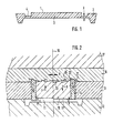
- Fig. 1 shows the sectional view a molding 1 made of plastic with different Wall thicknesses.
- the fitting 1 is rotationally symmetrical built up. It has an outer ring 2, which reinforces executed and profiled so that he at the later use in an annular housing groove can be attached.
- Inside the fitting 1 is a circular bottom or a membrane 3 with increased wall thickness provided.
- Fig. 2 shows a schematically shown Injection mold with which the molded part sketched in Fig. 1 1 can be manufactured.
- the injection mold shown includes in itself known manner, a first molded part or a mold plate 12 and a second molded part or a molded plate 13, with the help of not shown device elements moved along the center line 10 to open the mold can be.
- a molding space 11 or 11 ' In the illustrated closed Position define the molded parts 12, 13 between them a molding space 11 or 11 '.
- the molding space 11, 11 'in the embodiment shown is rotationally symmetrical is arranged to the center line 10 is the Invention on such a position of the mold space of course not limited. Others cannot either symmetrical arrangements are provided.
- Embodiment in molded part 13 is an arrangement consisting of an outer core member 14 and an inner stamp member 15 provided.
- the Elements 14, 15 can be relative to one another and to Molded part 13 are moved and have free end faces, that delimit the molding space 11 in some areas or define.
- the injection mold serves in the present embodiment the injection mold to make one disc-shaped molded part with an annular Cross-section thinning near its outer circumference.
- the outer core element 14 can consequently be cylindrical Have an axis configuration that coincides with the center line 10 of the mold space 11.
- the outer core member 14 is as indicated by the arrows 5, 6 indicated, between a first and second position relative to the opposite molded part 12 movable, each by suitable, not shown Appropriations are limited.
- the molding space 11 has a configuration in this position of the core element 14, which is essentially that of the one to be manufactured Fitting without reducing the wall thickness corresponds and is therefore also the starting mold space below 11 'designated.
- control element 16 in the direction arrow 9 can be by any suitable actuator (not shown), e.g. B. piston cylinder device, depending on the command one, too control device, not shown.
- suitable actuator e.g. B. piston cylinder device, depending on the command one, too control device, not shown.
- the arrangement of the interacting first Wedge surfaces 21, 22 is such that when the Control 16 in one direction (in the drawing to the right) the core element 14 the first or starting position takes while moving of the control element 16 in the opposite direction the core element 14 in the second, in the drawing left-hand, position is brought.
- a second pair of interacting wedge surfaces 23, 24 is on the inner stamp element 15 or Control element 16 is provided.
- the second wedge surfaces 23, 24 are in relation to the first wedge surfaces 21, 22 oppositely oriented so that the movement of the Control 16 movement in one direction of the stamp element 15 triggers in a direction that is opposite to that of the core element 14. at a displacement of the control element 16 in the Drawing to the left therefore experiences the stamp element 5 a movement in the direction of arrow 7 away from the opposite molded part 12, so that the Distance between the free end face of the stamp element 15 and the opposite wall area the mold space 11 slightly enlarged, while at the same time the distance between the free end face of the core element 14 the opposite wall area of the mold space 11 is reduced.
- the operation of the device described above is as follows. Not about that in the drawing The central sprue system shown becomes molten Plastic material injected into the starting mold space 11 ', whereby the core element 14 and stamp element 15 in the positions on the right in the drawing located so that the material without essential Disability due to the large gap "S" to the outer regions of the initial mold space 11 ' can flow and therefore its problem-free complete Filling is guaranteed. Immediately after completion the filling process is initiated by the control device Command to the actuating device of the control element 16 supplied, due to which the control 16 in one direction to the left in the drawing is moved along the arrow 9.
- the movement of the Control element 16 has the consequence that the core element 14 in the direction of arrow 5 in the second, in the drawing left-hand position is brought and the between its face and the opposite Wall of the mold space 11 displaced material becomes.
- the shift of the Control element 16 a movement of the inner stamp element 15 in a direction along arrow 7 away from the opposite molded part 12, whereby the distance between its free face and the opposite wall of the molding space 11 somewhat enlarged by that displaced by the core element 14 Volume.
- the Number of core and stamp elements 14, 15 shown and their arrangement among themselves and in relation to the mold space 11 are not limited, but any one Arrangement of one or more wall thickness reducing Core elements 14 with one or more stamp elements 15 can be provided.
- a stamp element 15 can be used to change the volume also be provided that through the core element 14 displaced material volume due to the still plastic Soul of the material in the mold space is led back into the sprue system.
- Others one Volume change-managing facilities, e.g. B. a membrane-like flexibility of a wall area of the mold space can also be provided his.
- the invention is on such a direction of movement is not restricted. Rather, the movements of the individual elements between their respective end positions adapted to the respective application and different be aligned.
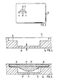
- FIG. 3 shows a chip card blank 26, which with the help of the procedure in particular can be produced advantageously.
- the blank card 26 has a recess 27 with the steps 28 and 33 in which a chip module at a later time is used.
- Fig. 4 the section A-B of Fig. 3 is schematic played. Because of the better overview dispenses with the exact reproduction of the proportions.
- the outer dimensions are usually such Chip cards about 85 mm x 54 mm, the thickness is 0.76 mm, the membrane 28 has at the bottom of the recess 27 a wall thickness of about 100 m.
- the outer The diameter of the recess 27 is approximately 15-20 mm, the shape of the recess can both in terms of outer outline as well as in the gradation arbitrarily vary. So z. B. rectangular, square or also known as oval outer outline.
- the deepening itself can also have several gradations or be lenticular in the inner region.
- Fig. 5 shows the section A-B of the map area with inserted chip module 44.
- the chip module exists thereby from a carrier film 29 on which metallic contact surfaces 30 are provided, via which at Use of the chip card 26 with the in the cast resin pill 31 arranged integrated circuit, or short Called chip (not shown) can.
- the chip module 44 has an adhesive layer 32 with the help of which the module is fixed in the Cutout 27 takes place.
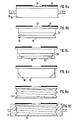
- Fig. 6 shows an injection mold for the production of Chip cards using the method according to the invention.
- the device consists essentially of a lower mold half 35 and an upper mold half 36. Between these two mold halves is the Molding space 38 provided the shape of the later Has a chip card, but without the one shown in FIG. 4 Indentation 27.
- the two mold halves 35 and 36 have an injection channel 39 through which the plastic material flows into the form.
- Stamp guide 46 provided over which the stamp 40 can be inserted into the mold space 38.
- the device shown in Fig. 6 has more Device elements, with the help of which in addition to the Production of the chip card blank described in the introduction also the simultaneous embedding of the chip module is possible.
- the upper mold half 36 is one more Guide plate 37 supplemented, which is also a stamp guide 46 has.
- the stamp 40 can thus through the guide plate 37 and the upper mold half 36 are pressed into the mold space.
- a transport channel 34 is provided, which Stamp guide 46 crosses and over the film tape 41 transported past the face of the stamp 40 can be.
- the film strip 41 is an "endless strip" executed and contains the chip modules lined up 44th
- stamp 40 no gradation, but a flat surface on.
- Suction air channels 43 are also provided, with the help of the film strip be sucked into the face of the stamp can.
- the film strip 41 is made in this way the end face of the stamp 40 arranged that a Chip card module 44 is positioned in front of it.
- the punch 40 By Lowering the punch 40 in the direction of the molding space 38 (Arrow 42) the chip module in the stamp guide of the Molded part 36 pressed and punched out of the film strip 41.
- the die-cut chip module is over the Suction channels 43 sucked in and thus on the end face of the stamp held.
- the stamp 40 is now ready lowered in the direction of the molding space 38, that the lower edge of the chip module approximately with the upper edge of the Forms 38 completes, d. H. the chip module still does not protrude into the mold space.
- the plastic material is injected via the injection channel 39. After sufficient filling of the mold space is the stamp together with the chip module in the Plastic compound pressed in so far that the flat end face of the stamp 40 flush with the later Card surface completes.
- the mold is opened, i.e. H. the mold halves 35 and 36 moved apart and by renewed Activate the stamp 40 ejected from the mold.
- the separation of the card from that in the injection channel 39 located plastic mass takes place in a known manner either by tearing it off or cutting it off with the help of cutting elements, not shown.
- the stamp 40 After closing the two mold halves 35 and 36, the stamp 40 is retracted into the starting position and the one with the punched-out 45 Area of the film tape moved on until again Chip module 44 is positioned in front of the stamp 40.
- the card manufacturing process shown in Fig. 6 thus enables the production of injection molded chip cards with simultaneous embedding of the chip module. Pressing the chip module into the injected one Tests have shown that plastic mass is relative unproblematic, as long as the outer shape of the chip module simply structured and the module mechanical is resilient. For complex structured modules or also when using large chip components (such as microprocessor chips) it may be advisable before embedding the module in the cavity Create card. This is done in a simple manner in that the process sequence described for FIG. 6 modified and a stamp 40 is used with to accomplish these additional functions are.
- stamp 40 shows a possible embodiment of a such equipped with additional functions Stamp 40.
- the stamp 40 consists of three one inside the other sliding stamp elements 47, 48 and 49.
- the Stamp 40 becomes in the form shown in Fig. 7a Pressing the recess 27 used. For this the Stamp through the foil punching 45 of the foil strip 41 brought through to the mold space 38, the plastic material is injected into the mold space and, as described initially, in the molding compound pressed.
- the stamp is 40 in the guide plate 37 withdrawn. Besides, will the stamp element 48 moves back until the end face of element 48 with the end face of the element 49 ends flush. Furthermore, the pin 47 in the position shown in Fig. 7b withdrawn and fixed. In this position there is a in the center of the Air channel opening into the face of the stamp, through a Bore in element 48 and one provided in element 49 Longitudinal groove 50 suctioning the chip module 44 allowed.
- the stamp 40 After the stamp 40 by withdrawing the Elements 47 and 48 in the arrangement shown in Fig. 7b brought and the film strip 41 by a position has been moved, the stamp 40 is again in the direction Formraum printed, being, as at the beginning a chip module 44 from the film strip 41 punched out and this in the previously created graded Placement placed. That with an adhesive layer 32 equipped chip module 44 is now with the stamp 40 pressed into the recess 27. The residual heat of the plastic material activates the hot glue and fixes it the module in the card body.
- the mold halves can 35 and 36 are opened again and the Card body can be removed from the form.
- chip modules with anchoring elements that Module in addition or as an alternative to an adhesive layer in anchor the card body are chip modules with anchoring elements that Module in addition or as an alternative to an adhesive layer in anchor the card body.
- Such a module is already from DE 31 31 216 C2 known and shown in Fig. 8a.
- the chip module exists a carrier film 29 on which contact surfaces 30 lie, which are conductively connected to the chip.
- To the Protection against mechanical loads are chip module and conductive connections from a cast body 55 surround.
- Anchoring elements protrude over the edge of the cast body 55 56, which is exclusively the Anchor the module in the card body.
- the anchoring element 56 as perforated ring to be formed in the map material is to be embedded.
- the holes are penetrated by the map material, so that the chip module is anchored in the card is guaranteed.
- Fig. 8c is a chip module with both recesses in the lateral surface as well as in the end face of the Cast body shown.
- the recess 59 in the lateral surface is ring-shaped and prevents Remove the chip module from the card body.
- the angled recesses 60 anchor the module additionally in the card body, but prevent beyond also twisting the module in the card.
- FIG. 8d shows a chip module, the cast body 55 thereof is penetrated by channels 58.
- the channels open on the one hand in the bottom surface of the module and on the other hand in the outer surface of the cast body.
- the channels point for example, an inclination of approximately 45 °.
- the in Fig. 8d chip module is particularly suitable if the module into the already injected plastic compound to be pressed in, since the channels 58 are also present very good from the still liquid plastic material be flowed through.
- the openings are to prevent use of the card arranged in the lateral surface so that they at pressed chip module positioned approximately in the middle of the card are. The ones that appear here with the card bent Forces are minimal, causing damage to the anchor by bending the card is not expected.
- FIG. 8e shows a chip module with a cast body 55, the outer surface of which is designed as a thread.
- the comparatively complex thread structure forms by pressing the module into the not yet solidified plastic mass as an exact negative form.
- the cast body and the card body educational materials chosen so that they are not connect with each other this can be done with the thread module anchored to the card body later from this be unscrewed.
- the invention Process of making a smart card with exchangeable module, without additional process steps to have to provide.
- FIG. 8f shows the module shown in FIG. 8e 55 in connection with a threaded sleeve 61.
- the sleeve has anchoring elements 56, via which the sleeve can be fixed in the card body.
- the sleeve 61 is either with or without screwed-in module 55 during the injection process into the card body brought in. To prevent the sleeve from deforming, is the insertion together with the chip module or a corresponding module dummy preferable.
- the sleeve 61 shown in Fig. 8f is with an anchoring frame equipped, as shown in Fig. 8a is. This protrudes beyond the edge of the sleeve 61 and ensures particularly good anchoring of the unit Chip module / sleeve in the card body.
- other anchoring elements are also wise usable such. B. those shown in Figs. 8b - 8e. Instead of the thread in this embodiment another detachable connection, such as. Legs Type bayonet lock, can be selected.
- Standard card 65 with an integrated mini chip card 66 as for example from DE 40 07 221 A1 is known.
- mini chip cards 66 are usually made of conventional standard cards 65 punched out.
- Standard card 65 with integrated mini chip card 66 can also with the help of the invention Injection molding process without subsequent punching processes getting produced. This is, for example, that in FIG. 6 Modify the injection mold shown.
- Fig. 10 shows such an adapted injection mold.
- the Stamping tool 69 has the shape of the in Fig. 9 in the Standard card 65 shown punching gap 75.
- stamping tool 69 closes the effective face of the Stamping tool 69 with the surface of the molding space the lower mold half 35 flush.
- the Stamping tool 69 is in the lower mold half 35 fitted so that it is with the help of the gripper 74 can be inserted into the mold space that but there is no gap over which it enters the mold space injected plastic compound can escape.
- the End face of the punch 69 are at the points where the connecting webs 67 should be generated, "notches" provided in Shape and size of the later connecting bars correspond.
- the production of the norm cards with integrated Mini chip cards are made in the usual way, i. H. like in 6 and 7 explained.
- the punch 69 pressed into the mold space with the aid of the grippers 74 to produce the outline 75 and the webs 67.
- the punching tool solidifies the card material removed with the grippers 74 from the mold space 38 and after opening the injection mold the card taken.
Landscapes
- Engineering & Computer Science (AREA)
- Computer Hardware Design (AREA)
- Microelectronics & Electronic Packaging (AREA)
- General Physics & Mathematics (AREA)
- Mechanical Engineering (AREA)
- Physics & Mathematics (AREA)
- Manufacturing & Machinery (AREA)
- Theoretical Computer Science (AREA)
- Injection Moulding Of Plastics Or The Like (AREA)
- Moulds For Moulding Plastics Or The Like (AREA)
- Credit Cards Or The Like (AREA)
- Extrusion Moulding Of Plastics Or The Like (AREA)
- Processing And Handling Of Plastics And Other Materials For Molding In General (AREA)
- Casting Or Compression Moulding Of Plastics Or The Like (AREA)
Claims (10)
- Procédé de fabrication de cartes à puce, formées par un corps de carte (26) moulé par injection, avec un évidement (27), dans lequel se trouve un module de puce (44), caractérisé par les étapes de procédé suivantes :positionnement d'une bande de feuille (41), munie de modules de puce (44), devant la surface frontale d'un poinçon (40) mobile,aspiration de la bande de feuille (41) par actionnement d'une source d'air d'aspiration dans la direction du poinçon (40),abaissement du poinçon (40) en direction d'un espace de moulage initial (38), dont la configuration correspond pour l'essentiel au corps de carte sans évidement et, simultanément, découpe d'un module (44) dans la bande de feuille (41),positionnement du module de puce (44) au niveau de la surface limite de l'espace de moulage initial (38),injection d'une matière plastique en fusion liquide dans l'espace de moulage initial (38),mouvement supplémentaire d'abaissement du poinçon (40), moyennant quoi le module de puce (44) est enfoncé dans la surface de la pièce moulée, après que l'espace de moulage (38) a été largement rempli dans la zone du poinçon (40) par 1a matière plastique,remplissage complet par injection de l'espace de moulage (38), dans la mesure où il reste encore dans l'espace de moulage (38) des vides à combler avec la matière plastique,refroidissement de la pièce moulée jusqu'à solidification de la matière plastique,ouverture du moule d'injection et démoulage de la pièce moulée.
- Procédé de fabrication de cartes à puce, formées par un corps de carte (26), moulé par injection, avec un évidement (27), dans lequel se trouve le module de puce (44), caractérisé par les étapes de procédé suivantes :abaissement d'un poinçon (40), avec une surface frontale adaptée à l'évidement à réaliser, jusque dans la zone de la surface de moulage d'un espace de moulage initial (38) dont la configuration correspond pour l'essentiel au corps de carte sans évidement,injection de la matière plastique dans l'espace de moulage initial (38),mouvement supplémentaire d'abaissement du poinçon (40) dans la masse formée par la matière plastique dans l'espace de moulage (38), en vue de former l'évidement à réaliser dans la pièce moulée,poursuite de l'injection de matière plastique jusqu'à ce que tous les vides dans l'espace de moulage (38) soient comblés,refroidissement de la pièce moulée jusqu'à solidification de la masse de matière plastique,mouvement de retour du poinçon (40) dans une position d'attente, dans laquelle une bande de feuille (41) munie de modules de puce (44) peut être positionnée devant la surface frontale du poinçon (40),modification de la surface frontale du poinçon dans une forme qui est adaptée à la découpe, à la fixation et à l'encartage d'un module de puce (44) dans le logement de la pièce moulée,positionnement de la bande de feuille (41) devant la surface frontale du poinçon (40),aspiration du module de puce (44),mouvement supplémentaire d'abaissement du poinçon (40) et, simultanément, découpe du module de puce (44), jusqu'à ce que le module de puce (44) soit inséré dans l'évidement de la pièce moulée ;enfoncement du module de puce (44) dans l'évidement (27) du corps de carte (26),ouverture du moule et démoulage de la carte à puce.
- Procédé selon l'une quelconque des revendications 1 et 2, caractérisé en ce que le poinçon (40) mobile est abaissé dans l'espace de moulage initial (38) uniquement après que celui-ci a été sensiblement rempli intégralement.
- Procédé selon la revendication 3, caractérisé en ce que, parallèlement à l'abaissement du poinçon (40) mobile ou à la diminution de certaines zones de paroi dans d'autres zones de l'espace de moulage (38), des distances entre parois sont agrandies, moyennant quoi les zones avec les distances entre parois agrandies sont destinées à recevoir la matière plastique refoulée hors des premières zones mentionnées.
- Procédé selon la revendication 3, caractérisé en ce que la matière est refoulée dans le système du culot d'injection (39).
- Procédé selon l'une quelconque des revendications 1 et 2, caractérisé en ce que le refoulement de matière provoqué par l'abaissement du poinçon (40) mobile dans l'espace de moulage (38) est déjà pris en compte au moment de l'admission de la matière.
- Procédé selon l'une quelconque des revendications 1 et 2, caractérisé en ce que le module de puce (44) est revêtu d'une couche thermocollante qui, après l'encartage dans l'évidement (27) ou après l'enfoncement dans la masse de matière plastique du corps de carte (26), est activée par l'intermédiaire de la chaleur résiduelle du corps de carte (26).
- Procédé de fabrication d'une minicarte à puce (66), intégrée dans une carte standard (65), qui est assemblée par des languettes (67) avec le corps de carte environnant de la carte standard (65), selon l'une quelconque des revendications 1 et 2, caractérisé en ce que les contours de la minicarte à puce (66) sont obtenus par l'enfoncement d'un outil d'estampage (69) dans la matière plastique contenue dans l'espace de moulage (38) du dispositif de moulage par injection.
- Dispositif de moulage par injection destiné à la mise en oeuvre du procédé selon la revendication 1, qui comprend au moins un espace de moulage et qui comporte des parties de moule mobiles l'une par rapport à l'autre et comporte au moins un poinçon mobile entre une première position et une deuxième position à l'intérieur et en dehors de la zone de moulage, caractérisé en ce quel'espace de moulage (38) correspond pour l'essentiel à une carte à puce sans évidement,l'une des parties du moule (35, 36) comporte un guidage (34) pour une bande de feuille (41) munie de modules de puce (44),la surface frontale du poinçon (40) mobile est essentiellement plane.
- Dispositif de moulage par injection destiné à la mise en oeuvre du procédé selon la revendication 2, qui comprend au moins un espace de moulage et qui comporte des parties de moule mobiles l'une par rapport à l'autre et comporte au moins un poinçon mobile entre une première position et une deuxième position à l'intérieur et en dehors de la zone de moulage, caractérisé en ce quel'espace de moulage (38) correspond pour l'essentiel à une carte à puce sans évidement,l'une des parties du moule (35, 36) comporte un guidage (34) pour une bande de feuille (41) munie de modules de puce (44),la surface frontale du poinçon (40) mobile est variable et correspond soit à l'évidement (27) à réaliser dans le corps de carte (22), soit présente une configuration essentiellement plane.
Applications Claiming Priority (5)
| Application Number | Priority Date | Filing Date | Title |
|---|---|---|---|
| DE4115208 | 1991-05-10 | ||
| DE4115208A DE4115208C2 (de) | 1991-05-10 | 1991-05-10 | Verfahren und Vorrichtung zum Herstellen von Kunststoff-Formstücken mit bereichsweise reduzierter Wandstärke |
| DE4142392 | 1991-12-20 | ||
| DE4142392A DE4142392C2 (de) | 1991-12-20 | 1991-12-20 | Verfahren und Vorrichtung zum Herstellen von spritzgegossenen Chipkarten mit bereichsweise reduzierter Wandstärke |
| PCT/EP1992/000991 WO1992020506A1 (fr) | 1991-05-10 | 1992-05-07 | Procede et dispositif de fabrication de pieces moulees en matiere plastique ayant des regions de paroi a epaisseur reduite |
Publications (3)
| Publication Number | Publication Date |
|---|---|
| EP0584143A1 EP0584143A1 (fr) | 1994-03-02 |
| EP0584143B1 EP0584143B1 (fr) | 1996-01-17 |
| EP0584143B2 true EP0584143B2 (fr) | 2003-04-16 |
Family
ID=25903497
Family Applications (1)
| Application Number | Title | Priority Date | Filing Date |
|---|---|---|---|
| EP92909860A Expired - Lifetime EP0584143B2 (fr) | 1991-05-10 | 1992-05-07 | Procede et dispositif de fabrication de pieces moulees en matiere plastique ayant des regions de paroi a epaisseur reduite |
Country Status (10)
| Country | Link |
|---|---|
| US (1) | US5681356A (fr) |
| EP (1) | EP0584143B2 (fr) |
| JP (1) | JP3290986B2 (fr) |
| AT (1) | ATE133105T1 (fr) |
| DE (1) | DE59205116D1 (fr) |
| DK (1) | DK0584143T3 (fr) |
| ES (1) | ES2082470T5 (fr) |
| GR (1) | GR3018955T3 (fr) |
| HK (1) | HK1007705A1 (fr) |
| WO (1) | WO1992020506A1 (fr) |
Families Citing this family (43)
| Publication number | Priority date | Publication date | Assignee | Title |
|---|---|---|---|---|
| US5476629A (en) * | 1992-12-25 | 1995-12-19 | Citizen Watch Co. Ltd. | Method for manufacturing IC card substrate |
| DE4401588C2 (de) * | 1994-01-20 | 2003-02-20 | Gemplus Gmbh | Verfahren zum Verkappen eines Chipkarten-Moduls und Chipkarten-Modul |
| ES2102317B1 (es) * | 1994-09-19 | 1998-04-16 | Nacional Moneda Timbre | Tarjeta inteligente de uso en telefonia y similar. |
| FR2735714B1 (fr) * | 1995-06-21 | 1997-07-25 | Schlumberger Ind Sa | Procede pour imprimer un graphisme sur une carte a memoire |
| US5975584A (en) * | 1996-08-30 | 1999-11-02 | Adaptech S.A. | Carrier card with value chip |
| ATE210864T1 (de) * | 1996-10-09 | 2001-12-15 | Pav Card Gmbh | Verfahren und verbindungsanordnung zum herstellen einer chipkarte |
| US5823071A (en) * | 1996-10-31 | 1998-10-20 | Borg-Warner Automotive, Inc. | Integrated transmission control system |
| DE19703122C1 (de) * | 1997-01-29 | 1998-05-20 | Orga Kartensysteme Gmbh | Verfahren zur Herstellung von Datenträgern |
| DE19736082C1 (de) * | 1997-08-20 | 1999-01-14 | Orga Kartensysteme Gmbh | Verfahren und Herstellen einer Chipkarte und Vorrichtung zur Durchführung des Verfahrens |
| FR2778002B1 (fr) * | 1998-04-22 | 2000-06-30 | Gemplus Card Int | Procede de fabrication d'une carte a circuit integre a contact et une carte obtenue selon ce procede |
| ATE288600T1 (de) * | 1999-08-12 | 2005-02-15 | Ovd Kinegram Ag | Datenträger |
| JP4606553B2 (ja) * | 2000-08-11 | 2011-01-05 | 大日本印刷株式会社 | カード状基材の製造用金型およびカード状基材の製造方法 |
| US6923378B2 (en) * | 2000-12-22 | 2005-08-02 | Digimarc Id Systems | Identification card |
| US6588099B2 (en) * | 2001-01-22 | 2003-07-08 | Sankyo Kasei Kabushiki Kaisha | Process for manufacturing molded circuit board |
| WO2002066226A1 (fr) * | 2001-02-22 | 2002-08-29 | Tele-Cd Company A/S | Procede de production d'un disque optique avec module detachable |
| EP1249330A1 (fr) * | 2001-04-12 | 2002-10-16 | Dynamit Nobel Kunststoff GmbH | Procédé de fabrication d'une pièce en matière plastique et pièce |
| US6817530B2 (en) | 2001-12-18 | 2004-11-16 | Digimarc Id Systems | Multiple image security features for identification documents and methods of making same |
| FR2834103B1 (fr) * | 2001-12-20 | 2004-04-02 | Gemplus Card Int | Carte a puce a module de surface etendue |
| WO2003056499A2 (fr) * | 2001-12-24 | 2003-07-10 | Digimarc Id Systems Llc | Cartes a puce a contact ayant un noyau document et cartes a puce sans contact comprenant une structure multicouche, un document d'identification a base de pet, et leurs procedes de production |
| ATE552120T1 (de) | 2001-12-24 | 2012-04-15 | L 1 Secure Credentialing Inc | Verdeckte variableninformationen auf id- dokumenten und verfahren zu ihrer herstellung |
| US7728048B2 (en) | 2002-12-20 | 2010-06-01 | L-1 Secure Credentialing, Inc. | Increasing thermal conductivity of host polymer used with laser engraving methods and compositions |
| WO2003055638A1 (fr) | 2001-12-24 | 2003-07-10 | Digimarc Id Systems, Llc | Elements de securite grave au laser destines a des documents d'identification et procedes de fabrication de ces elements |
| US7694887B2 (en) | 2001-12-24 | 2010-04-13 | L-1 Secure Credentialing, Inc. | Optically variable personalized indicia for identification documents |
| US7815124B2 (en) | 2002-04-09 | 2010-10-19 | L-1 Secure Credentialing, Inc. | Image processing techniques for printing identification cards and documents |
| US7793846B2 (en) | 2001-12-24 | 2010-09-14 | L-1 Secure Credentialing, Inc. | Systems, compositions, and methods for full color laser engraving of ID documents |
| US7824029B2 (en) | 2002-05-10 | 2010-11-02 | L-1 Secure Credentialing, Inc. | Identification card printer-assembler for over the counter card issuing |
| US7804982B2 (en) | 2002-11-26 | 2010-09-28 | L-1 Secure Credentialing, Inc. | Systems and methods for managing and detecting fraud in image databases used with identification documents |
| DE602004030434D1 (de) | 2003-04-16 | 2011-01-20 | L 1 Secure Credentialing Inc | Dreidimensionale datenspeicherung |
| US7744002B2 (en) | 2004-03-11 | 2010-06-29 | L-1 Secure Credentialing, Inc. | Tamper evident adhesive and identification document including same |
| DE102007062459B4 (de) | 2007-12-22 | 2022-10-27 | Leuze Electronic Gmbh + Co. Kg | Vorrichtung zum Verbinden zweier optischer und/oder elektronischer Bauteile |
| EP2633970B1 (fr) * | 2010-10-29 | 2016-01-06 | Konica Minolta, Inc. | Matrice de formage, micropuce fabriquée à l'aude d'une matrice et appareil de fabrication d'une micropuce |
| NO348516B1 (no) * | 2013-04-30 | 2025-02-24 | Sinvent As | En fremgangsmåte for fremstilling av et lab-på-brikke-system og et lab-på-brikke-system |
| GB2544717B (en) * | 2015-09-25 | 2019-04-10 | Gr8 Eng Ltd | Injection Molding Method |
| DE102015119235B4 (de) * | 2015-11-09 | 2019-01-10 | Selectrona GmbH | Vorrichtung zum Spritzgießen und Umspritzen von Objekten |
| US10977540B2 (en) | 2016-07-27 | 2021-04-13 | Composecure, Llc | RFID device |
| US11267172B2 (en) | 2016-07-27 | 2022-03-08 | Composecure, Llc | Overmolded electronic components for transaction cards and methods of making thereof |
| US11618191B2 (en) | 2016-07-27 | 2023-04-04 | Composecure, Llc | DI metal transaction devices and processes for the manufacture thereof |
| US10762412B2 (en) | 2018-01-30 | 2020-09-01 | Composecure, Llc | DI capacitive embedded metal card |
| US11151437B2 (en) | 2017-09-07 | 2021-10-19 | Composecure, Llc | Metal, ceramic, or ceramic-coated transaction card with window or window pattern and optional backlighting |
| SG11202002064SA (en) | 2017-09-07 | 2020-04-29 | Composecure Llc | Transaction card with embedded electronic components and process for manufacture |
| HUE060022T2 (hu) | 2017-10-18 | 2023-01-28 | Composecure Llc | Fém, kerámia vagy kerámiabevonatos tranzakciókártya ablakkal vagy ablakmintával és opcionális háttévilágítással |
| USD948613S1 (en) | 2020-04-27 | 2022-04-12 | Composecure, Llc | Layer of a transaction card |
| DE102021210271A1 (de) * | 2021-09-16 | 2023-03-16 | Magna Exteriors Gmbh | Verfahren zum Herstellen von Kunststoffbauteilen |
Family Cites Families (23)
| Publication number | Priority date | Publication date | Assignee | Title |
|---|---|---|---|---|
| US3030666A (en) * | 1960-01-07 | 1962-04-24 | Owens Illinois Glass Co | Method for low pressure molding |
| DE1729368A1 (de) * | 1967-10-13 | 1971-06-09 | Per Thorkildsen | Verfahren und Vorrichtung zur Herstellung von dekorierten,spritzgegossenen Plastgegenstaenden |
| US4184835A (en) * | 1978-09-28 | 1980-01-22 | General Electric Company | Mold apparatus |
| DE3029667A1 (de) * | 1980-08-05 | 1982-03-11 | GAO Gesellschaft für Automation und Organisation mbH, 8000 München | Traegerelement fuer einen ic-baustein |
| JPS6058010B2 (ja) * | 1981-04-14 | 1985-12-18 | 三井化学株式会社 | 射出圧縮成形方法 |
| DE3153768C2 (de) * | 1981-04-14 | 1995-11-09 | Gao Ges Automation Org | Ausweiskarte |
| US4470786A (en) * | 1981-07-28 | 1984-09-11 | Omron Tateisi Electronics Co. | Molding apparatus with retractable preform support pins |
| JPS5839425A (ja) * | 1981-09-04 | 1983-03-08 | Hashimoto Forming Co Ltd | 低圧射出成形法 |
| FR2520541A1 (fr) * | 1982-01-22 | 1983-07-29 | Flonic Sa | Procede d'insertion d'un circuit integre dans une carte a memoire et carte obtenue suivant ce procede |
| DD230476A3 (de) * | 1983-03-25 | 1985-12-04 | Schwarzenberg Waschgeraete | Verfahren zur herstellung von spritzgussteilen mit aussparungen |
| JPS59185636A (ja) * | 1983-04-08 | 1984-10-22 | Ricoh Co Ltd | 射出圧縮成形法 |
| US4540534A (en) * | 1983-10-11 | 1985-09-10 | American Optical Corporation | Apparatus and method for injection molding lenses |
| JPS60193347A (ja) * | 1984-03-15 | 1985-10-01 | Toshiba Corp | 半導体製造装置 |
| JPS6168209A (ja) * | 1984-09-12 | 1986-04-08 | Aisin Seiki Co Ltd | ポリアミド成形品の成形加工法 |
| FR2579799B1 (fr) * | 1985-03-28 | 1990-06-22 | Flonic Sa | Procede de fabrication de cartes a memoire electronique et cartes obtenues suivant ledit procede |
| JPS6213094A (ja) * | 1985-07-10 | 1987-01-21 | 三井化学株式会社 | 配線用プリント基板の製法及びその装置 |
| FR2599165A1 (fr) * | 1986-05-21 | 1987-11-27 | Michot Gerard | Objet associe a un element electronique et procede d'obtention |
| US4980115A (en) * | 1987-05-28 | 1990-12-25 | Yoshida Industry Co. Ltd. | Method for making an injection-molded product having a partly thin portion |
| US5304513A (en) * | 1987-07-16 | 1994-04-19 | Gao Gesellschaft Fur Automation Und Organisation Mbh | Method for manufacturing an encapsulated semiconductor package using an adhesive barrier frame |
| US4954308A (en) * | 1988-03-04 | 1990-09-04 | Citizen Watch Co., Ltd. | Resin encapsulating method |
| US4961893A (en) * | 1988-04-28 | 1990-10-09 | Schlumberger Industries | Method for manufacturing memory cards |
| US4944908A (en) * | 1988-10-28 | 1990-07-31 | Eaton Corporation | Method for forming a molded plastic article |
| US5417905A (en) * | 1989-05-26 | 1995-05-23 | Esec (Far East) Limited | Method of making a card having decorations on both faces |
-
1992
- 1992-05-07 DE DE59205116T patent/DE59205116D1/de not_active Expired - Fee Related
- 1992-05-07 US US08/146,087 patent/US5681356A/en not_active Expired - Fee Related
- 1992-05-07 EP EP92909860A patent/EP0584143B2/fr not_active Expired - Lifetime
- 1992-05-07 DK DK92909860.6T patent/DK0584143T3/da active
- 1992-05-07 AT AT92909860T patent/ATE133105T1/de not_active IP Right Cessation
- 1992-05-07 ES ES92909860T patent/ES2082470T5/es not_active Expired - Lifetime
- 1992-05-07 JP JP50898592A patent/JP3290986B2/ja not_active Expired - Fee Related
- 1992-05-07 WO PCT/EP1992/000991 patent/WO1992020506A1/fr not_active Ceased
-
1996
- 1996-02-14 GR GR960400356T patent/GR3018955T3/el unknown
-
1998
- 1998-06-26 HK HK98106916A patent/HK1007705A1/xx not_active IP Right Cessation
Also Published As
| Publication number | Publication date |
|---|---|
| GR3018955T3 (en) | 1996-05-31 |
| JP3290986B2 (ja) | 2002-06-10 |
| DE59205116D1 (de) | 1996-02-29 |
| WO1992020506A1 (fr) | 1992-11-26 |
| ATE133105T1 (de) | 1996-02-15 |
| EP0584143A1 (fr) | 1994-03-02 |
| EP0584143B1 (fr) | 1996-01-17 |
| HK1007705A1 (en) | 1999-04-23 |
| ES2082470T3 (es) | 1996-03-16 |
| DK0584143T3 (da) | 1996-02-12 |
| JPH06507126A (ja) | 1994-08-11 |
| ES2082470T5 (es) | 2003-12-16 |
| US5681356A (en) | 1997-10-28 |
Similar Documents
| Publication | Publication Date | Title |
|---|---|---|
| EP0584143B2 (fr) | Procede et dispositif de fabrication de pieces moulees en matiere plastique ayant des regions de paroi a epaisseur reduite | |
| DE69414292T2 (de) | Verfahren und Vorrichtung zum Herstellen einer Speicherkarte | |
| DE69013220T2 (de) | Herstellungsverfahren einer Chipkarte und Karte, erhalten nach diesem Verfahren. | |
| EP0709805B1 (fr) | Méthode de fabrication de porteurs d'informations incorporant des éléments et dispositif de mise en oeuvre de la méthode | |
| DE69527746T2 (de) | Verfahren zur Einbettung eines Dekors, insbesondere Textil, in einem Kunststoffteil | |
| DE69212895T3 (de) | Spritzgiessverfahren, Vorrichtung und spritzgegossenes Teil | |
| EP0791448A2 (fr) | Procédé et dispositif pour mouler par injection des articles en matière plastique | |
| DE2342794B2 (de) | Verfahren und Vorrichtung zum diskontinuierlichen Herstellen von Mehrschicht-Formteilen aus thermoplastischem Kunststoff | |
| EP1938944A1 (fr) | Procédé pour la fabrication d'un corps en matière plastique multicouche | |
| DE2537801A1 (de) | Puppenkopf und verfahren zu dessen herstellung | |
| DE4142392C2 (de) | Verfahren und Vorrichtung zum Herstellen von spritzgegossenen Chipkarten mit bereichsweise reduzierter Wandstärke | |
| DE3113071C2 (fr) | ||
| DE19729486C2 (de) | Verfahren zur Herstellung eines Kunststoffteiles und Vorrichtung zur Durchführung des Verfahrens | |
| DE4142410C2 (de) | Vorrichtung zum Herstellen von flachen Kunststoff-Formstücken, beispielsweise Ausweiskarten durch Spritzgießen | |
| DE69716507T2 (de) | Verfahren zur Verkleidung eines Kunststoffteiles mit einer während des Verfahrens geschnittenen Folie und hergestellter Teil | |
| EP0419953A2 (fr) | Dispositif pour le moulage par injection en deux couches | |
| DE19646184A1 (de) | Verfahren zum Herstellen einer Chipkarte und Vorrichtung zum Durchführen des Verfahrens | |
| DE19749243C1 (de) | Verfahren und Vorrichtung zum Herstellen von Verbundkörpern aus einer Kunststoffmasse | |
| DE19736082C1 (de) | Verfahren und Herstellen einer Chipkarte und Vorrichtung zur Durchführung des Verfahrens | |
| EP0419829A2 (fr) | Procédé et dispositif pour fabriquer des récipients pour produits alimentaires et similaires | |
| DE69811791T2 (de) | Verfahren und Form zum Herstellen eines bekleideten Kunstoffgegenstandes mit einer geschnittenen und entspannten Dekorfolie. | |
| DE19617768C2 (de) | Verfahren und Vorrichtung zum Spritzgießen von Kunststoffteilen | |
| EP1358992A1 (fr) | Moule d'injection pour fabriquer une carte à puce ainsi que procédé pour fabriquer une carte à puce | |
| DE4115208C2 (de) | Verfahren und Vorrichtung zum Herstellen von Kunststoff-Formstücken mit bereichsweise reduzierter Wandstärke | |
| DE19750344C2 (de) | Verfahren zum Herstellen eines flachen Kartengrundkörpers für eine Chipkarte |
Legal Events
| Date | Code | Title | Description |
|---|---|---|---|
| PUAI | Public reference made under article 153(3) epc to a published international application that has entered the european phase |
Free format text: ORIGINAL CODE: 0009012 |
|
| 17P | Request for examination filed |
Effective date: 19931008 |
|
| AK | Designated contracting states |
Kind code of ref document: A1 Designated state(s): AT BE CH DE DK ES FR GB GR IT LI LU MC NL SE |
|
| 17Q | First examination report despatched |
Effective date: 19941219 |
|
| GRAA | (expected) grant |
Free format text: ORIGINAL CODE: 0009210 |
|
| AK | Designated contracting states |
Kind code of ref document: B1 Designated state(s): AT BE CH DE DK ES FR GB GR IT LI LU MC NL SE |
|
| PG25 | Lapsed in a contracting state [announced via postgrant information from national office to epo] |
Ref country code: NL Free format text: LAPSE BECAUSE OF FAILURE TO SUBMIT A TRANSLATION OF THE DESCRIPTION OR TO PAY THE FEE WITHIN THE PRESCRIBED TIME-LIMIT Effective date: 19960117 |
|
| REF | Corresponds to: |
Ref document number: 133105 Country of ref document: AT Date of ref document: 19960215 Kind code of ref document: T |
|
| ITF | It: translation for a ep patent filed | ||
| REG | Reference to a national code |
Ref country code: DK Ref legal event code: T3 |
|
| GBT | Gb: translation of ep patent filed (gb section 77(6)(a)/1977) |
Effective date: 19960122 |
|
| REF | Corresponds to: |
Ref document number: 59205116 Country of ref document: DE Date of ref document: 19960229 |
|
| ET | Fr: translation filed | ||
| REG | Reference to a national code |
Ref country code: ES Ref legal event code: FG2A Ref document number: 2082470 Country of ref document: ES Kind code of ref document: T3 |
|
| REG | Reference to a national code |
Ref country code: CH Ref legal event code: NV Representative=s name: SCHAAD, BALASS & PARTNER AG |
|
| REG | Reference to a national code |
Ref country code: GR Ref legal event code: FG4A Free format text: 3018955 |
|
| PLBI | Opposition filed |
Free format text: ORIGINAL CODE: 0009260 |
|
| PLBQ | Unpublished change to opponent data |
Free format text: ORIGINAL CODE: EPIDOS OPPO |
|
| PLBI | Opposition filed |
Free format text: ORIGINAL CODE: 0009260 |
|
| PLAV | Examination of admissibility of opposition |
Free format text: ORIGINAL CODE: EPIDOS OPEX |
|
| PLAV | Examination of admissibility of opposition |
Free format text: ORIGINAL CODE: EPIDOS OPEX |
|
| PLAV | Examination of admissibility of opposition |
Free format text: ORIGINAL CODE: EPIDOS OPEX |
|
| 26 | Opposition filed |
Opponent name: GEMPLUS, GEMENOS ATT. M. NONNENMACHER Effective date: 19961017 |
|
| 26 | Opposition filed |
Opponent name: GPT AXXICON B.V. Effective date: 19961017 Opponent name: GEMPLUS, GEMENOS ATT. M. NONNENMACHER Effective date: 19961017 |
|
| PLBF | Reply of patent proprietor to notice(s) of opposition |
Free format text: ORIGINAL CODE: EPIDOS OBSO |
|
| PLBF | Reply of patent proprietor to notice(s) of opposition |
Free format text: ORIGINAL CODE: EPIDOS OBSO |
|
| NLR1 | Nl: opposition has been filed with the epo |
Opponent name: GEMPLUS, GEMENOS ATT. M. NONNENMACHER |
|
| NLR1 | Nl: opposition has been filed with the epo |
Opponent name: GPT AXXICON B.V. Opponent name: GEMPLUS, GEMENOS ATT. M. NONNENMACHER |
|
| PLBF | Reply of patent proprietor to notice(s) of opposition |
Free format text: ORIGINAL CODE: EPIDOS OBSO |
|
| PLBF | Reply of patent proprietor to notice(s) of opposition |
Free format text: ORIGINAL CODE: EPIDOS OBSO |
|
| RDAH | Patent revoked |
Free format text: ORIGINAL CODE: EPIDOS REVO |
|
| APAC | Appeal dossier modified |
Free format text: ORIGINAL CODE: EPIDOS NOAPO |
|
| APAE | Appeal reference modified |
Free format text: ORIGINAL CODE: EPIDOS REFNO |
|
| APAC | Appeal dossier modified |
Free format text: ORIGINAL CODE: EPIDOS NOAPO |
|
| REG | Reference to a national code |
Ref country code: GB Ref legal event code: IF02 |
|
| PGFP | Annual fee paid to national office [announced via postgrant information from national office to epo] |
Ref country code: NL Payment date: 20020517 Year of fee payment: 11 |
|
| PGFP | Annual fee paid to national office [announced via postgrant information from national office to epo] |
Ref country code: LU Payment date: 20020523 Year of fee payment: 11 Ref country code: DK Payment date: 20020523 Year of fee payment: 11 Ref country code: AT Payment date: 20020523 Year of fee payment: 11 |
|
| PGFP | Annual fee paid to national office [announced via postgrant information from national office to epo] |
Ref country code: GR Payment date: 20020524 Year of fee payment: 11 Ref country code: SE Payment date: 20020524 Year of fee payment: 11 Ref country code: MC Payment date: 20020524 Year of fee payment: 11 Ref country code: CH Payment date: 20020524 Year of fee payment: 11 |
|
| APAC | Appeal dossier modified |
Free format text: ORIGINAL CODE: EPIDOS NOAPO |
|
| PLAW | Interlocutory decision in opposition |
Free format text: ORIGINAL CODE: EPIDOS IDOP |
|
| PUAH | Patent maintained in amended form |
Free format text: ORIGINAL CODE: 0009272 |
|
| 27A | Patent maintained in amended form |
Effective date: 20030416 |
|
| AK | Designated contracting states |
Designated state(s): AT BE CH DE DK ES FR GB GR IT LI LU MC NL SE |
|
| PG25 | Lapsed in a contracting state [announced via postgrant information from national office to epo] |
Ref country code: LU Free format text: LAPSE BECAUSE OF NON-PAYMENT OF DUE FEES Effective date: 20030507 Ref country code: AT Free format text: LAPSE BECAUSE OF NON-PAYMENT OF DUE FEES Effective date: 20030507 |
|
| PG25 | Lapsed in a contracting state [announced via postgrant information from national office to epo] |
Ref country code: SE Free format text: LAPSE BECAUSE OF NON-PAYMENT OF DUE FEES Effective date: 20030508 |
|
| GBTA | Gb: translation of amended ep patent filed (gb section 77(6)(b)/1977) | ||
| REG | Reference to a national code |
Ref country code: CH Ref legal event code: AEN Free format text: AUFRECHTERHALTUNG DES PATENTES IN GEAENDERTER FORM |
|
| PG25 | Lapsed in a contracting state [announced via postgrant information from national office to epo] |
Ref country code: MC Free format text: LAPSE BECAUSE OF NON-PAYMENT OF DUE FEES Effective date: 20030531 Ref country code: LI Free format text: LAPSE BECAUSE OF NON-PAYMENT OF DUE FEES Effective date: 20030531 Ref country code: CH Free format text: LAPSE BECAUSE OF NON-PAYMENT OF DUE FEES Effective date: 20030531 |
|
| PG25 | Lapsed in a contracting state [announced via postgrant information from national office to epo] |
Ref country code: DK Free format text: LAPSE BECAUSE OF FAILURE TO SUBMIT A TRANSLATION OF THE DESCRIPTION OR TO PAY THE FEE WITHIN THE PRESCRIBED TIME-LIMIT Effective date: 20030716 |
|
| PG25 | Lapsed in a contracting state [announced via postgrant information from national office to epo] |
Ref country code: GR Free format text: THE PATENT HAS BEEN ANNULLED BY A DECISION OF A NATIONAL AUTHORITY Effective date: 20030804 |
|
| NLV1 | Nl: lapsed or annulled due to failure to fulfill the requirements of art. 29p and 29m of the patents act | ||
| ET3 | Fr: translation filed ** decision concerning opposition | ||
| REG | Reference to a national code |
Ref country code: ES Ref legal event code: DC2A Date of ref document: 20030704 Kind code of ref document: T5 |
|
| EUG | Se: european patent has lapsed | ||
| REG | Reference to a national code |
Ref country code: CH Ref legal event code: PL |
|
| PGFP | Annual fee paid to national office [announced via postgrant information from national office to epo] |
Ref country code: GB Payment date: 20040426 Year of fee payment: 13 |
|
| PGFP | Annual fee paid to national office [announced via postgrant information from national office to epo] |
Ref country code: BE Payment date: 20040525 Year of fee payment: 13 |
|
| PG25 | Lapsed in a contracting state [announced via postgrant information from national office to epo] |
Ref country code: GB Free format text: LAPSE BECAUSE OF NON-PAYMENT OF DUE FEES Effective date: 20050507 |
|
| PG25 | Lapsed in a contracting state [announced via postgrant information from national office to epo] |
Ref country code: BE Free format text: LAPSE BECAUSE OF NON-PAYMENT OF DUE FEES Effective date: 20050531 |
|
| APAH | Appeal reference modified |
Free format text: ORIGINAL CODE: EPIDOSCREFNO |
|
| BERE | Be: lapsed |
Owner name: G.- FUR AUTOMATION UND ORGANISATION M.B.H. *GAO Effective date: 20050531 |
|
| GBPC | Gb: european patent ceased through non-payment of renewal fee |
Effective date: 20050507 |
|
| PGFP | Annual fee paid to national office [announced via postgrant information from national office to epo] |
Ref country code: IT Payment date: 20060531 Year of fee payment: 15 |
|
| PGFP | Annual fee paid to national office [announced via postgrant information from national office to epo] |
Ref country code: ES Payment date: 20070620 Year of fee payment: 16 |
|
| BERE | Be: lapsed |
Owner name: G.- FUR AUTOMATION UND ORGANISATION M.B.H. *GAO Effective date: 20050531 |
|
| REG | Reference to a national code |
Ref country code: ES Ref legal event code: FD2A Effective date: 20080508 |
|
| PGFP | Annual fee paid to national office [announced via postgrant information from national office to epo] |
Ref country code: FR Payment date: 20090519 Year of fee payment: 18 |
|
| PG25 | Lapsed in a contracting state [announced via postgrant information from national office to epo] |
Ref country code: IT Free format text: LAPSE BECAUSE OF NON-PAYMENT OF DUE FEES Effective date: 20070507 |
|
| PG25 | Lapsed in a contracting state [announced via postgrant information from national office to epo] |
Ref country code: ES Free format text: LAPSE BECAUSE OF NON-PAYMENT OF DUE FEES Effective date: 20080508 |
|
| PGFP | Annual fee paid to national office [announced via postgrant information from national office to epo] |
Ref country code: DE Payment date: 20090729 Year of fee payment: 18 |
|
| REG | Reference to a national code |
Ref country code: FR Ref legal event code: ST Effective date: 20110131 |
|
| PG25 | Lapsed in a contracting state [announced via postgrant information from national office to epo] |
Ref country code: DE Free format text: LAPSE BECAUSE OF NON-PAYMENT OF DUE FEES Effective date: 20101201 |
|
| PG25 | Lapsed in a contracting state [announced via postgrant information from national office to epo] |
Ref country code: FR Free format text: LAPSE BECAUSE OF NON-PAYMENT OF DUE FEES Effective date: 20100531 |