EP0585640A2 - Herstellungsverfahren von einem Kontakt für eine Halbleiteranordnung - Google Patents
Herstellungsverfahren von einem Kontakt für eine Halbleiteranordnung Download PDFInfo
- Publication number
- EP0585640A2 EP0585640A2 EP93112505A EP93112505A EP0585640A2 EP 0585640 A2 EP0585640 A2 EP 0585640A2 EP 93112505 A EP93112505 A EP 93112505A EP 93112505 A EP93112505 A EP 93112505A EP 0585640 A2 EP0585640 A2 EP 0585640A2
- Authority
- EP
- European Patent Office
- Prior art keywords
- layer
- polysilicon
- silicon dioxide
- over
- doped
- Prior art date
- Legal status (The legal status is an assumption and is not a legal conclusion. Google has not performed a legal analysis and makes no representation as to the accuracy of the status listed.)
- Granted
Links
Images

Classifications
-
- H—ELECTRICITY
- H10—SEMICONDUCTOR DEVICES; ELECTRIC SOLID-STATE DEVICES NOT OTHERWISE PROVIDED FOR
- H10W—GENERIC PACKAGES, INTERCONNECTIONS, CONNECTORS OR OTHER CONSTRUCTIONAL DETAILS OF DEVICES COVERED BY CLASS H10
- H10W20/00—Interconnections in chips, wafers or substrates
- H10W20/01—Manufacture or treatment
- H10W20/071—Manufacture or treatment of dielectric parts thereof
- H10W20/081—Manufacture or treatment of dielectric parts thereof by forming openings in the dielectric parts
-
- H—ELECTRICITY
- H10—SEMICONDUCTOR DEVICES; ELECTRIC SOLID-STATE DEVICES NOT OTHERWISE PROVIDED FOR
- H10W—GENERIC PACKAGES, INTERCONNECTIONS, CONNECTORS OR OTHER CONSTRUCTIONAL DETAILS OF DEVICES COVERED BY CLASS H10
- H10W20/00—Interconnections in chips, wafers or substrates
- H10W20/01—Manufacture or treatment
- H10W20/031—Manufacture or treatment of conductive parts of the interconnections
- H10W20/063—Manufacture or treatment of conductive parts of the interconnections by forming conductive members before forming protective insulating material
-
- H—ELECTRICITY
- H10—SEMICONDUCTOR DEVICES; ELECTRIC SOLID-STATE DEVICES NOT OTHERWISE PROVIDED FOR
- H10W—GENERIC PACKAGES, INTERCONNECTIONS, CONNECTORS OR OTHER CONSTRUCTIONAL DETAILS OF DEVICES COVERED BY CLASS H10
- H10W20/00—Interconnections in chips, wafers or substrates
- H10W20/01—Manufacture or treatment
- H10W20/031—Manufacture or treatment of conductive parts of the interconnections
- H10W20/069—Manufacture or treatment of conductive parts of the interconnections by forming self-aligned vias or self-aligned contact plugs
-
- H—ELECTRICITY
- H10—SEMICONDUCTOR DEVICES; ELECTRIC SOLID-STATE DEVICES NOT OTHERWISE PROVIDED FOR
- H10W—GENERIC PACKAGES, INTERCONNECTIONS, CONNECTORS OR OTHER CONSTRUCTIONAL DETAILS OF DEVICES COVERED BY CLASS H10
- H10W20/00—Interconnections in chips, wafers or substrates
- H10W20/01—Manufacture or treatment
- H10W20/071—Manufacture or treatment of dielectric parts thereof
- H10W20/074—Manufacture or treatment of dielectric parts thereof of dielectric parts comprising thin functional dielectric layers, e.g. dielectric etch-stop, barrier, capping or liner layers
- H10W20/076—Manufacture or treatment of dielectric parts thereof of dielectric parts comprising thin functional dielectric layers, e.g. dielectric etch-stop, barrier, capping or liner layers in via holes or trenches
-
- H—ELECTRICITY
- H10—SEMICONDUCTOR DEVICES; ELECTRIC SOLID-STATE DEVICES NOT OTHERWISE PROVIDED FOR
- H10W—GENERIC PACKAGES, INTERCONNECTIONS, CONNECTORS OR OTHER CONSTRUCTIONAL DETAILS OF DEVICES COVERED BY CLASS H10
- H10W20/00—Interconnections in chips, wafers or substrates
- H10W20/01—Manufacture or treatment
- H10W20/071—Manufacture or treatment of dielectric parts thereof
- H10W20/074—Manufacture or treatment of dielectric parts thereof of dielectric parts comprising thin functional dielectric layers, e.g. dielectric etch-stop, barrier, capping or liner layers
- H10W20/077—Manufacture or treatment of dielectric parts thereof of dielectric parts comprising thin functional dielectric layers, e.g. dielectric etch-stop, barrier, capping or liner layers on sidewalls or on top surfaces of conductors
-
- H—ELECTRICITY
- H10—SEMICONDUCTOR DEVICES; ELECTRIC SOLID-STATE DEVICES NOT OTHERWISE PROVIDED FOR
- H10W—GENERIC PACKAGES, INTERCONNECTIONS, CONNECTORS OR OTHER CONSTRUCTIONAL DETAILS OF DEVICES COVERED BY CLASS H10
- H10W20/00—Interconnections in chips, wafers or substrates
- H10W20/40—Interconnections external to wafers or substrates, e.g. back-end-of-line [BEOL] metallisations or vias connecting to gate electrodes
- H10W20/41—Interconnections external to wafers or substrates, e.g. back-end-of-line [BEOL] metallisations or vias connecting to gate electrodes characterised by their conductive parts
- H10W20/44—Conductive materials thereof
- H10W20/4451—Semiconductor materials, e.g. polysilicon
Definitions
- the present invention relates to a method of making a conductive contact for a semiconductor device, and more particularly, to a method of making a capped and borderless contacts for semiconductor devices, such as integrated circuits.
- Contacts for semiconductor devices are conductive regions on a surface of a semiconductor body which make electrical contact to the body or conductive regions in the body. Capped contacts are those which are completely surrounded by insulating material. Borderless contacts are those which can overlap isolation or gate areas of semiconductor devices. For high density integrated circuits, such as dynamic random access memories (DRAMs), forming such capped and borderless contacts is very difficult, particularly in a full scale manufacturing process. Such contacts are, however, required for high density types of integrated circuits such as DRAMs. Especially the inner node contact from transfer transistor to storage electrode requires these capped and borderless contacts. Capping is necessary to allow other conducting layers to cross over the contact area as is e.g. required by bitlines in DRAM memories.
- DRAMs dynamic random access memories
- One technique for forming capped and borderless contacts is to form the contacts of doped polysilicon.
- the doped polysilicon contacts regions are formed in openings in undoped (intrinsic) polysilicon.
- the undoped polysilicon can easily be etched selective to gate encapsulations or isolations to allow overlap or borderlessness.
- the undoped polysilicon must then be removed and replaced with an insulating material of low dielectric constant, such as silicon dioxide.
- Standard masking systems for removing the undoped polysilicon without damaging the doped polysilicon contact regions are difficult to control or they require special selective etchants. Therefore, it is desirable to have a method of forming capped borderless doped polysilicon contacts which is relatively simple to carry out and can be readily used in a manufacturing process.
- An aspect of the present invention is directed to a method of making borderless contacts of doped polysilicon in openings in undoped polysilicon in which a self-aligned masking layer of silicon dioxide is formed over the doped polysilicon. This is achieved by thermally growing the silicon dioxide over both the doped and undoped polysilicon with the thickness of the silicon dioxide layer being greater over the doped polysilicon than over the undoped polysilicon. The thinner portions of the silicon dioxide layer over the undoped polysilicon can then be easily removed by etching while still leaving a portion of silicon dioxide over the doped polysilicon.
- the method of the present invention for making a semiconductor device conductive contact to a body of semiconductor material includes forming a layer of undoped polysilicon on a surface of the body. An opening is formed in the undoped polysilicon layer and the opening is filled with doped polysilicon. A layer of silicon dioxide is grown over both the undoped and doped polysilicon with the silicon dioxide layer over the doped polysilicon being thicker than over the undoped polysilicon. The thinner portions of the silicon dioxide layer over the undoped polysilicon are then removed leaving the silicon dioxide only over the doped polysilicon. The undoped polysilicon is then removed.
- the present invention is directed to a method of making a conductive contact to a surface of a body of a semiconductor material.
- the method comprises the steps of depositing on the surface of the body a layer of undoped polysilicon; forming an opening through the undoped polysilicon layer to the surface of the body; coating side walls of the opening with a layer of silicon nitride or another insulating film; filling the remaining portion of the opening with doped polysilicon; heating the doped and undoped polysilicon in an oxidizing atmosphere to grow a layer of silicon dioxide thereon which is thicker over the doped polysilicon than over the undoped polysilicon; etching the silicon dioxide layer so as to remove the portion thereof over the undoped polysilicon while leaving a portion of the silicon dioxide layer over the doped polysilicon; removing the undoped polysilicon; and forming a layer of a dielectric material on the body surface surrounding the doped polysilicon.
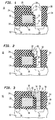
- FIGs. 1-6 are cross-sectional view of a semiconductor device, illustrating the various steps of the method of the present invention for forming a device with a borderless contact.
- FIG. 1 there is shown a cross-sectional view of a portion of a metal-oxide-semiconductor (MOS) field effect transistor (FET) 10 as it appears at the start of the method of the present invention for forming a borderless contact.
- the transistor 10 comprises a substrate body 12 of a semiconductor material, such as single crystalline silicon, having a surface 14.
- a gate 16 of a conductive material, such as conductive polysilicon is typically of silicon dioxide.
- the gate 16 is covered with an encapsulation layer 17, typically of silicon dioxide, and has sidewall spacers 19 along each side, also typically of silicon dioxide.
- the transistor 10 is an n-channel insulated gated field effect transistor (IGFET) with the body being of p-type conductivity and the source and drain regions 20 and 22, respectively, being of n-type conductivity.
- IGFET insulated gated field effect transistor
- the method of the present invention will be described with regard to forming a contact to the region 22. However, it should be understood that the method of the present invention can be used to form contacts to both of the regions 20 and 22 or to other regions formed in the body 12, such as buried capacitors of the type shown in U.S. Patent No. 4,927,779 (S. H. Dhong, issued May 22, 1990).
- the first step in the method of the present invention is to deposit a layer 24 of undoped (intrinsic) polysilicon over the body surface 14 and the gate 16.
- This can be achieved by the well known chemical vapor deposition technique in which the body 12 is exposed to a gas containing silicon, such as silane, and heated to decompose the gas and deposit polysilicon on the surface 14.
- a masking layer 26, such as of a photoresist, is coated over the polysilicon layer 24. Using standard photolithographic techniques, the masking layer 26 is provided with an opening 28 therein over the area of the body surface 14 where the contact is to be formed.
- the exposed portion of the polysilicon layer 24 is then removed using a suitable etchant to form an opening 30 therethrough down to the portion of surface 14 which includes a portion of the region 22.
- FIG. 2 there is shown a cross-sectional view of the transistor 10 during the next steps of the method of the present invention.
- the masking layer 26 is removed with a suitable solvent and then side walls of the opening 30 are coated with a layer 32 of silicon nitride or another insulating material. This is achieved by depositing a layer of silicon nitride over the polysilicon layer 24, the sidewalls of the opening 30 and the exposed area of the body surface 14 at the bottom of the opening 30.
- the portions of the silicon nitride layer which are on the polysilicon layer 24 and the body surface 14 at the bottom of the opening 30 are then removed with an anisotropic etch, such as a plasma etch. This leaves the silicon nitride layer 32 on the sidewalls of the opening 30.
- FIG. 3 there is shown a cross-sectional view of the transistor 10 after the next step in the method of the present invention.
- the opening 30 is then filled with doped polysilicon to form an electrical contact 34. This is achieved by depositing a layer of doped polysilicon over the undoped polysilicon layer 24 and within the opening 30. The portion of the doped polysilicon layer over the undoped layer 24 is then removed with a suitable etchant leaving the doped polysilicon contact 34 in the opening 30. During this etching step, the contact 34 may be provided with a shallow cavity 36 in its surface.
- the contact 34 is doped with any suitable dopant of the desired conductivity type, such as phosphorus for n-type conductivity.
- the contact 34 is preferably heavily doped to a concentration of about 5x10²⁰ impurities/cm3.
- the doped polysilicon may be deposited by any well known chemical vapor deposition technique in which the body 12 is exposed to vapors of a gas containing silicon, such a silane, and a gas containing the desired dopant. The body 12 is heated to a temperature at which the gases decompose and deposit doped polysilicon.
- FIG. 4 there is shown a cross-sectional view of the transistor 10 after the next step in the method of the present invention.
- the polysilicon layer 24 and contact 34 are then heated in an oxidizing atmosphere at a temperature at which a silicon dioxide layer 38 is formed on the surfaces of the layer 24 and the contact 34. Typically, this can be carried out in steam at a temperature of between 700°C and 900°C.
- the silicon dioxide film formed on doped polysilicon is thicker than the silicon dioxide film formed on undoped polysilicon.
- a portion 40 of the silicon dioxide layer 36 directly over the contact 34, which is of doped polysilicon, is thicker than a portion 42 of the silicon dioxide layer 38 which is over the undoped polysilicon layer 24.
- the thickness of the thicker portion 40 of the silicon dioxide layer 36 can be made more than twice the thickness of the thinner portion 42.
- FIG. 5 there is shown a cross-sectional view of the transistor 10 after the next step of the method of the present invention.
- the silicon dioxide layer 38 is then etched with a suitable etchant until the thinner portion 42 of the silicon dioxide layer 38 is completely removed from over the undoped polysilicon layer 24. Although the thicker portion 42 of the silicon dioxide layer 38 is reduced in thickness, a portion still remains to provide a capping layer over the contact 34 which is self-aligned with the contact 34.
- the exposed portion of the undoped polysilicon layer 24 is then removed with a suitable etchant. During this etching step, the contact 34 is protected from being etched by the capping portion 40 of the layer 38 and by the sidewall silicon nitride layers 32.
- a layer 44 of a dielectric material such as silicon dioxide
- a layer 44 of a dielectric material is then deposited over the gate 16 and the exposed area of the surface 14 so as to completely encircle the contact 34.
- the silicon dioxide layer is then planarized, using any well known planarization technique, to form the layer 44 which encircles the contact 34 and has a surface which is planar with the surface of the contact 34.
- This provides the transistor 10 with a conductive contact 34 which can provide lateral contact to other areas such as e.g. trench capacitors (not shown in the drawing).
- the contact is borderless and capped so that the contact is isolated from crossing conductor lines. This is important since the same technique can be used to form other contacts which contact to these crossing conductor lines. Bitlines of DRAM cells are an example.
- the method of the present invention by using the difference in the oxidation rate of doped and undoped polysilicon, a self-aligned capping layer 40 of silicon dioxide is easily formed over the contact 34.
- the self-aligned capping layer 40 along with the sidewall spacers silicon nitride layers 30 around the contact 34, protect the contact 34 during the removal of the undoped polysilicon layer 24 and its replacement with the dielectric layer 44. This allows the removal of the undoped polysilicon layer 24 with the use of any standard etchant which simplifies the removal of the undoped polysilicon layer.
- the method of the present invention provides a simple method of forming borderless contacts which can be used as part of a manufacturing process for integrated circuits containing the contacts.
- the contact can be made to any device formed in the substrate body.
- the device can include any desired number of the contacts as well as conductive strips connecting the contacts.
Landscapes
- Electrodes Of Semiconductors (AREA)
- Internal Circuitry In Semiconductor Integrated Circuit Devices (AREA)
- Formation Of Insulating Films (AREA)
- Conductive Materials (AREA)
- Die Bonding (AREA)
Applications Claiming Priority (2)
| Application Number | Priority Date | Filing Date | Title |
|---|---|---|---|
| US93792192A | 1992-08-31 | 1992-08-31 | |
| US937921 | 1992-08-31 |
Publications (3)
| Publication Number | Publication Date |
|---|---|
| EP0585640A2 true EP0585640A2 (de) | 1994-03-09 |
| EP0585640A3 EP0585640A3 (de) | 1994-11-09 |
| EP0585640B1 EP0585640B1 (de) | 1998-11-11 |
Family
ID=25470571
Family Applications (1)
| Application Number | Title | Priority Date | Filing Date |
|---|---|---|---|
| EP93112505A Expired - Lifetime EP0585640B1 (de) | 1992-08-31 | 1993-08-04 | Verfahren zur Herstellung eines leitenden Kontakts auf einem Halbleiterkörper |
Country Status (7)
| Country | Link |
|---|---|
| US (1) | US5464793A (de) |
| EP (1) | EP0585640B1 (de) |
| JP (1) | JPH0824111B2 (de) |
| KR (2) | KR100290691B1 (de) |
| AT (1) | ATE173357T1 (de) |
| DE (1) | DE69322024T2 (de) |
| TW (1) | TW214610B (de) |
Families Citing this family (9)
| Publication number | Priority date | Publication date | Assignee | Title |
|---|---|---|---|---|
| JP2720796B2 (ja) * | 1994-11-15 | 1998-03-04 | 日本電気株式会社 | 半導体装置の製造方法 |
| US5627103A (en) * | 1995-03-02 | 1997-05-06 | Sony Corporation | Method of thin film transistor formation with split polysilicon deposition |
| US6103572A (en) * | 1997-02-07 | 2000-08-15 | Citizen Watch Co., Ltd. | Method of fabricating a semiconductor nonvolatile storage device |
| WO1999004427A1 (de) * | 1997-07-15 | 1999-01-28 | Infineon Technologies Ag | Kontaktierung einer halbleiterzone |
| JP3090198B2 (ja) * | 1997-08-21 | 2000-09-18 | 日本電気株式会社 | 半導体装置の構造およびその製造方法 |
| US6057216A (en) * | 1997-12-09 | 2000-05-02 | International Business Machines Corporation | Low temperature diffusion process for dopant concentration enhancement |
| US6215190B1 (en) * | 1998-05-12 | 2001-04-10 | International Business Machines Corporation | Borderless contact to diffusion with respect to gate conductor and methods for fabricating |
| US6261924B1 (en) | 2000-01-21 | 2001-07-17 | Infineon Technologies Ag | Maskless process for self-aligned contacts |
| US6940134B2 (en) * | 2002-07-02 | 2005-09-06 | International Business Machines Corporation | Semiconductor with contact contacting diffusion adjacent gate electrode |
Family Cites Families (8)
| Publication number | Priority date | Publication date | Assignee | Title |
|---|---|---|---|---|
| GB1388926A (en) * | 1972-03-04 | 1975-03-26 | Ferranti Ltd | Manufacture of silicon semiconductor devices |
| US4127931A (en) * | 1974-10-04 | 1978-12-05 | Nippon Electric Co., Ltd. | Semiconductor device |
| JPS5922380B2 (ja) * | 1975-12-03 | 1984-05-26 | 株式会社東芝 | ハンドウタイソシノ セイゾウホウホウ |
| JPS54158167A (en) * | 1978-06-05 | 1979-12-13 | Toshiba Corp | Manufacture of semiconductor device |
| US4694561A (en) * | 1984-11-30 | 1987-09-22 | American Telephone And Telegraph Company, At&T Bell Laboratories | Method of making high-performance trench capacitors for DRAM cells |
| US4717678A (en) * | 1986-03-07 | 1988-01-05 | International Business Machines Corporation | Method of forming self-aligned P contact |
| US4927779A (en) * | 1988-08-10 | 1990-05-22 | International Business Machines Corporation | Complementary metal-oxide-semiconductor transistor and one-capacitor dynamic-random-access memory cell and fabrication process therefor |
| US5198386A (en) * | 1992-06-08 | 1993-03-30 | Micron Technology, Inc. | Method of making stacked capacitors for DRAM cell |
-
1993
- 1993-04-20 TW TW082102998A patent/TW214610B/zh not_active IP Right Cessation
- 1993-06-25 JP JP5179854A patent/JPH0824111B2/ja not_active Expired - Lifetime
- 1993-08-04 AT AT93112505T patent/ATE173357T1/de not_active IP Right Cessation
- 1993-08-04 DE DE69322024T patent/DE69322024T2/de not_active Expired - Lifetime
- 1993-08-04 EP EP93112505A patent/EP0585640B1/de not_active Expired - Lifetime
- 1993-08-31 KR KR1019930017088A patent/KR100290691B1/ko not_active Expired - Fee Related
-
1994
- 1994-10-03 US US08/317,151 patent/US5464793A/en not_active Expired - Lifetime
-
2000
- 2000-09-18 KR KR1020000054689A patent/KR100363295B1/ko not_active Expired - Fee Related
Also Published As
| Publication number | Publication date |
|---|---|
| DE69322024D1 (de) | 1998-12-17 |
| KR100363295B1 (ko) | 2002-12-05 |
| DE69322024T2 (de) | 1999-04-08 |
| EP0585640A3 (de) | 1994-11-09 |
| TW214610B (en) | 1993-10-11 |
| JPH0824111B2 (ja) | 1996-03-06 |
| ATE173357T1 (de) | 1998-11-15 |
| KR940004728A (ko) | 1994-03-15 |
| EP0585640B1 (de) | 1998-11-11 |
| JPH06112152A (ja) | 1994-04-22 |
| US5464793A (en) | 1995-11-07 |
| KR100290691B1 (ko) | 2001-06-01 |
Similar Documents
| Publication | Publication Date | Title |
|---|---|---|
| US5780338A (en) | Method for manufacturing crown-shaped capacitors for dynamic random access memory integrated circuits | |
| US4462040A (en) | Single electrode U-MOSFET random access memory | |
| US5324673A (en) | Method of formation of vertical transistor | |
| US4252579A (en) | Method for making single electrode U-MOSFET random access memory utilizing reactive ion etching and polycrystalline deposition | |
| US5670404A (en) | Method for making self-aligned bit line contacts on a DRAM circuit having a planarized insulating layer | |
| US4742018A (en) | Process for producing memory cell having stacked capacitor | |
| US6261899B1 (en) | Semiconductor processing methods of forming integrated circuitry memory devices, methods of forming capacitor containers, methods of making electrical connection to circuit nodes and related integrated circuitry | |
| US6008084A (en) | Method for fabricating low resistance bit line structures, along with bit line structures exhibiting low bit line to bit line coupling capacitance | |
| US5874359A (en) | Small contacts for ultra large scale integration semiconductor devices without separation ground rule | |
| US6326295B1 (en) | Method and structure for improved alignment tolerance in multiple, singulated plugs and interconnection | |
| US6165823A (en) | Thin film transistor and a fabricating method therefor | |
| US5436190A (en) | Method for fabricating semiconductor device isolation using double oxide spacers | |
| EP0977256A2 (de) | Verfahren zur Herstellung eines DRAM-Grabenkondensators | |
| KR19980063505A (ko) | 트렌치 캐패시터 및 그의 형성 방법과, 디램 저장 셀 형성 방법 | |
| US20070128776A1 (en) | Isolated fully depleted silicon-on-insulator regions by selective etch | |
| US6137130A (en) | Capacitor over bit line structure using a straight bit line shape | |
| US6406987B1 (en) | Method for making borderless contacts to active device regions and overlaying shallow trench isolation regions | |
| US6319772B1 (en) | Method for making low-leakage DRAM structures using selective silicon epitaxial growth (SEG) on an insulating layer | |
| US5464793A (en) | Method of making contact for semiconductor device | |
| US5849625A (en) | Planar field oxide isolation process for semiconductor integrated circuit devices using liquid phase deposition | |
| KR20010014111A (ko) | 측부가 유전적으로 절연된 반도체 디바이스를 형성하는방법 및 이 방법에 의해 제조된 모스 반도체 디바이스 | |
| US20020094628A1 (en) | Integrated circuit having at least two vertical MOS transistors and method for manufacturing same | |
| US20050020008A1 (en) | Collar formation using selective SiGe/Si etch | |
| HK1003753A (en) | Method of making contact for semiconductor device | |
| KR100426492B1 (ko) | 반도체소자의전하저장전극형성방법 |
Legal Events
| Date | Code | Title | Description |
|---|---|---|---|
| PUAI | Public reference made under article 153(3) epc to a published international application that has entered the european phase |
Free format text: ORIGINAL CODE: 0009012 |
|
| AK | Designated contracting states |
Kind code of ref document: A2 Designated state(s): AT DE FR GB IE IT NL |
|
| PUAL | Search report despatched |
Free format text: ORIGINAL CODE: 0009013 |
|
| AK | Designated contracting states |
Kind code of ref document: A3 Designated state(s): AT DE FR GB IE IT NL |
|
| 17P | Request for examination filed |
Effective date: 19950504 |
|
| 17Q | First examination report despatched |
Effective date: 19970515 |
|
| GRAG | Despatch of communication of intention to grant |
Free format text: ORIGINAL CODE: EPIDOS AGRA |
|
| GRAG | Despatch of communication of intention to grant |
Free format text: ORIGINAL CODE: EPIDOS AGRA |
|
| GRAH | Despatch of communication of intention to grant a patent |
Free format text: ORIGINAL CODE: EPIDOS IGRA |
|
| GRAH | Despatch of communication of intention to grant a patent |
Free format text: ORIGINAL CODE: EPIDOS IGRA |
|
| GRAA | (expected) grant |
Free format text: ORIGINAL CODE: 0009210 |
|
| AK | Designated contracting states |
Kind code of ref document: B1 Designated state(s): AT DE FR GB IE IT NL |
|
| PG25 | Lapsed in a contracting state [announced via postgrant information from national office to epo] |
Ref country code: NL Free format text: LAPSE BECAUSE OF FAILURE TO SUBMIT A TRANSLATION OF THE DESCRIPTION OR TO PAY THE FEE WITHIN THE PRESCRIBED TIME-LIMIT Effective date: 19981111 Ref country code: AT Free format text: LAPSE BECAUSE OF FAILURE TO SUBMIT A TRANSLATION OF THE DESCRIPTION OR TO PAY THE FEE WITHIN THE PRESCRIBED TIME-LIMIT Effective date: 19981111 |
|
| REF | Corresponds to: |
Ref document number: 173357 Country of ref document: AT Date of ref document: 19981115 Kind code of ref document: T |
|
| REF | Corresponds to: |
Ref document number: 69322024 Country of ref document: DE Date of ref document: 19981217 |
|
| REG | Reference to a national code |
Ref country code: IE Ref legal event code: FG4D |
|
| ET | Fr: translation filed | ||
| ITF | It: translation for a ep patent filed | ||
| NLV1 | Nl: lapsed or annulled due to failure to fulfill the requirements of art. 29p and 29m of the patents act | ||
| PLBE | No opposition filed within time limit |
Free format text: ORIGINAL CODE: 0009261 |
|
| 26N | No opposition filed | ||
| REG | Reference to a national code |
Ref country code: GB Ref legal event code: IF02 |
|
| REG | Reference to a national code |
Ref country code: HK Ref legal event code: WD Ref document number: 1003753 Country of ref document: HK |
|
| PGFP | Annual fee paid to national office [announced via postgrant information from national office to epo] |
Ref country code: GB Payment date: 20050725 Year of fee payment: 13 |
|
| GBPC | Gb: european patent ceased through non-payment of renewal fee |
Effective date: 20060804 |
|
| PG25 | Lapsed in a contracting state [announced via postgrant information from national office to epo] |
Ref country code: GB Free format text: LAPSE BECAUSE OF NON-PAYMENT OF DUE FEES Effective date: 20060804 |
|
| PGFP | Annual fee paid to national office [announced via postgrant information from national office to epo] |
Ref country code: DE Payment date: 20100914 Year of fee payment: 18 |
|
| REG | Reference to a national code |
Ref country code: FR Ref legal event code: TP Owner name: QIMONDA AG,, DE Effective date: 20120123 |
|
| PGFP | Annual fee paid to national office [announced via postgrant information from national office to epo] |
Ref country code: IE Payment date: 20120821 Year of fee payment: 20 |
|
| PGFP | Annual fee paid to national office [announced via postgrant information from national office to epo] |
Ref country code: IT Payment date: 20120822 Year of fee payment: 20 Ref country code: FR Payment date: 20120906 Year of fee payment: 20 |
|
| PG25 | Lapsed in a contracting state [announced via postgrant information from national office to epo] |
Ref country code: DE Free format text: LAPSE BECAUSE OF NON-PAYMENT OF DUE FEES Effective date: 20130301 |
|
| REG | Reference to a national code |
Ref country code: DE Ref legal event code: R119 Ref document number: 69322024 Country of ref document: DE Effective date: 20130301 |
|
| REG | Reference to a national code |
Ref country code: IE Ref legal event code: MK9A |
|
| PG25 | Lapsed in a contracting state [announced via postgrant information from national office to epo] |
Ref country code: IE Free format text: LAPSE BECAUSE OF EXPIRATION OF PROTECTION Effective date: 20130804 |