EP0586774B1 - Procédé de fabrication de films minces par déposition multicouche - Google Patents
Procédé de fabrication de films minces par déposition multicouche Download PDFInfo
- Publication number
- EP0586774B1 EP0586774B1 EP92810699A EP92810699A EP0586774B1 EP 0586774 B1 EP0586774 B1 EP 0586774B1 EP 92810699 A EP92810699 A EP 92810699A EP 92810699 A EP92810699 A EP 92810699A EP 0586774 B1 EP0586774 B1 EP 0586774B1
- Authority
- EP
- European Patent Office
- Prior art keywords
- deposition
- deposited
- accordance
- layer
- layers
- Prior art date
- Legal status (The legal status is an assumption and is not a legal conclusion. Google has not performed a legal analysis and makes no representation as to the accuracy of the status listed.)
- Expired - Lifetime
Links
Images


Classifications
-
- H—ELECTRICITY
- H10—SEMICONDUCTOR DEVICES; ELECTRIC SOLID-STATE DEVICES NOT OTHERWISE PROVIDED FOR
- H10N—ELECTRIC SOLID-STATE DEVICES NOT OTHERWISE PROVIDED FOR
- H10N60/00—Superconducting devices
- H10N60/01—Manufacture or treatment
- H10N60/0268—Manufacture or treatment of devices comprising copper oxide
- H10N60/0296—Processes for depositing or forming copper oxide superconductor layers
-
- H—ELECTRICITY
- H10—SEMICONDUCTOR DEVICES; ELECTRIC SOLID-STATE DEVICES NOT OTHERWISE PROVIDED FOR
- H10N—ELECTRIC SOLID-STATE DEVICES NOT OTHERWISE PROVIDED FOR
- H10N60/00—Superconducting devices
- H10N60/80—Constructional details
- H10N60/85—Superconducting active materials
- H10N60/855—Ceramic superconductors
- H10N60/857—Ceramic superconductors comprising copper oxide
-
- Y—GENERAL TAGGING OF NEW TECHNOLOGICAL DEVELOPMENTS; GENERAL TAGGING OF CROSS-SECTIONAL TECHNOLOGIES SPANNING OVER SEVERAL SECTIONS OF THE IPC; TECHNICAL SUBJECTS COVERED BY FORMER USPC CROSS-REFERENCE ART COLLECTIONS [XRACs] AND DIGESTS
- Y10—TECHNICAL SUBJECTS COVERED BY FORMER USPC
- Y10S—TECHNICAL SUBJECTS COVERED BY FORMER USPC CROSS-REFERENCE ART COLLECTIONS [XRACs] AND DIGESTS
- Y10S505/00—Superconductor technology: apparatus, material, process
- Y10S505/725—Process of making or treating high tc, above 30 k, superconducting shaped material, article, or device
- Y10S505/729—Growing single crystal, e.g. epitaxy, bulk
-
- Y—GENERAL TAGGING OF NEW TECHNOLOGICAL DEVELOPMENTS; GENERAL TAGGING OF CROSS-SECTIONAL TECHNOLOGIES SPANNING OVER SEVERAL SECTIONS OF THE IPC; TECHNICAL SUBJECTS COVERED BY FORMER USPC CROSS-REFERENCE ART COLLECTIONS [XRACs] AND DIGESTS
- Y10—TECHNICAL SUBJECTS COVERED BY FORMER USPC
- Y10S—TECHNICAL SUBJECTS COVERED BY FORMER USPC CROSS-REFERENCE ART COLLECTIONS [XRACs] AND DIGESTS
- Y10S505/00—Superconductor technology: apparatus, material, process
- Y10S505/725—Process of making or treating high tc, above 30 k, superconducting shaped material, article, or device
- Y10S505/73—Vacuum treating or coating
- Y10S505/731—Sputter coating
-
- Y—GENERAL TAGGING OF NEW TECHNOLOGICAL DEVELOPMENTS; GENERAL TAGGING OF CROSS-SECTIONAL TECHNOLOGIES SPANNING OVER SEVERAL SECTIONS OF THE IPC; TECHNICAL SUBJECTS COVERED BY FORMER USPC CROSS-REFERENCE ART COLLECTIONS [XRACs] AND DIGESTS
- Y10—TECHNICAL SUBJECTS COVERED BY FORMER USPC
- Y10S—TECHNICAL SUBJECTS COVERED BY FORMER USPC CROSS-REFERENCE ART COLLECTIONS [XRACs] AND DIGESTS
- Y10S505/00—Superconductor technology: apparatus, material, process
- Y10S505/725—Process of making or treating high tc, above 30 k, superconducting shaped material, article, or device
- Y10S505/73—Vacuum treating or coating
- Y10S505/732—Evaporative coating with superconducting material
-
- Y—GENERAL TAGGING OF NEW TECHNOLOGICAL DEVELOPMENTS; GENERAL TAGGING OF CROSS-SECTIONAL TECHNOLOGIES SPANNING OVER SEVERAL SECTIONS OF THE IPC; TECHNICAL SUBJECTS COVERED BY FORMER USPC CROSS-REFERENCE ART COLLECTIONS [XRACs] AND DIGESTS
- Y10—TECHNICAL SUBJECTS COVERED BY FORMER USPC
- Y10S—TECHNICAL SUBJECTS COVERED BY FORMER USPC CROSS-REFERENCE ART COLLECTIONS [XRACs] AND DIGESTS
- Y10S505/00—Superconductor technology: apparatus, material, process
- Y10S505/725—Process of making or treating high tc, above 30 k, superconducting shaped material, article, or device
- Y10S505/742—Annealing
Definitions
- the present invention relates to a process for manufacturing solid compounds of three or more different base materials. More particularly, it relates to a method for manufacturing high-T c -superconductors as thin films.
- Deposited onto said substrate or buffer layer are layers of base material, selected to form the high-T c -superconductor, using a variety of techniques like sputtering, laser ablation, co-evaporation and monolayer-by-monolayer deposition. These deposition techniques can roughly be divided into two different categories: either all materials necessary to build up the unit cell of the compound are deposited simultaneously, or the different base materials are deposited consecutively by piling up monolayers of the different base materials. As understood herein, a unit cell of an ideal crystal is an identical volume which completely fills the space of the crystal without any overlapping. A monolayer is the amount of an element or compound necessary to cover the entire surface of a substrate with a layer of single atoms or molecules, respectively.
- This technique is characterized by sequentially depositing layers of suitable base materials onto a heated substrate. In contrast to the monolayer-by-monolayer technique, the thickness of the layers is determined by the stoichiometric ratio of the compound to be produced.
- the thickness of a single layer lies within a range from 8nm to 100nm, corresponding to 30 to over 300 monolayers.
- the layers of different base materials are combined to a period of layers, a number of which may be repeatedly deposited until the desired thickness of the film is reached.
- the known multilayer deposition of thick layers requires an annealing step, during which the deposited layers are heated in an oxygen atmosphere. This annealing step is necessary to balance the deficiency in the oxygen content of the deposited layers to transform these layers into superconducting material. As the temperature of the substrate has to be increased substantially by more than 100 Kelvin, and often the vacuum chamber has to be changed to proceed, the known multilayer deposition technique is a relatively slow process.
- the annealing step further prevents an in-situ control over the growth of the desired compound. It is, therefore, an object of the present invention to overcome the above-mentioned problems and to provide a new process based on the multilayer deposition to manufacture thin films of solid compounds having crystal structure with improved qualities. Another object of the invention is to provide a method for producing films of high-T c -superconducting material showing an homogeneous crystal structure. It is a further object of the invention to provide a method for producing films having a smooth surface. Another important object of the invention is to eliminate the previously required annealing step from the manufacturing process of high-T c -superconducting material.
- the present invention provides a method for manufacturing thin films of solid compounds, especially high-T c -superconductors, by an improved periodic multilayer deposition technique, wherein the layer thickness is reduced and the crystallization of the compound takes place at approximately the same temperature as the deposition of the layers and before depositing a further period of layers.
- the thickness of a layer is reduced to one to twenty, preferably to two to ten monolayers. This corresponds to layer thicknesses of approximately 0,3nm to 6,0nm, and 0,6nm to 3,0nm, respectively.
- the number of monolayers within a single layer does not necessarily have to be an integer.
- a monolayer is primarily defined as an amount of material
- layers consisting of a fractional number of monolayers, e.g. 1,5 monolayers.
- Such a layer is also hereinafter referred to as block layer or bulk layer.
- the deposition is called periodic.
- a period is a fixed number of block layers of different base materials being repeatedly deposited.
- These layers preferably three to six, are sufficient to form the desired compound. It is nevertheless possible to manufacture a very thin film of the compound by depositing only one period of layers. But to manufacture more stable films, it is preferred to deposit at least two periods of layers.
- Typical compounds preferably produced in accordance with the new method are ceramic superconductors.
- the method may be used to manufacture superconductors as listed in EP-A-0426570, page 3, II. 36-55 and superconductors belonging to the "infinite layers" category, such as Ca 1-x Sr x CuO y , Sr 1-x Ln x CuO y with Ln standing for an element selected from the lanthanides, including yttrium and lanthanum, Ba 1-x Sr x CuO y , compounds of the above-mentioned category including dopants selected from the group comprising C, N, F, and Cl, or electron doped superconductors.
- the "infinite layers" category such as Ca 1-x Sr x CuO y , Sr 1-x Ln x CuO y with Ln standing for an element selected from the lanthanides, including yttrium and lanthanum, Ba 1-x Sr x CuO y , compounds of the above-mentioned category including dopants selected from the group comprising C, N, F,
- the new method can also be used to produce selenides, phosphides, nitrides, arsenides, or tellurides of CuZn, Culn or similar compounds.
- the stoichiometric ratio also known as atomic ratio, defines the thickness ratio of the layers within one deposition period.
- each deposition period will consist of a block layer or block of one or more monolayers of the first base material, a second block layer of twice as many monolayers of the second base material and a third block layer of the third base material consisting of thrice as many monolayers as the first block.
- each period in itself is sufficient for producing a layer of the desired compound almost free of impurities, compared with films produced by known techniques.
- the invention does not depend on any specific deposition method, it lies within the scope of any person skilled in the art to apply any of such methods. Methods well known in this technical field are for example sputtering, laser ablation, metal organic chemical vapor deposition (MOCVD), molecular beam epitaxy (MBE) and the like.
- MOCVD metal organic chemical vapor deposition
- MBE molecular beam epitaxy
- the first bulk layer or block serves as (intrinsic) buffer layer, itself.
- the proper selection of the order in which the layers are deposited improves the control over the crystal growth of the solid compound.
- the blocks or layers having a small diffusion coefficient are preferably deposited first, and the block consisting of base material with the greatest diffusion coefficient or length is deposited last.
- Cu or its oxide is preferably chosen as last layer.
- the crystallization process is initiated when all layers of one period, except the last, have been deposited with their correct stoichiometric ratio, i.e. the correct thickness by the start of the deposition of the last layer. Within one deposition period, the crystallization also ends with the last layer being deposited. As the last layer is also being deposited according to the correct stoichiometric ratio, the desired compound is accomplished without defects due to incorrect stoichiometry.
- the crystallization of the desired compound starts and ends with the deposition of the last layer within the deposition period.
- a seperate annealing step as used within the described multilayer deposition methods, becomes unnecessary.
- the desired compound e.g. a superconductor, is formed without a significant change in temperature.
- the temperature of the substrate or of the deposition chamber does not have to be changed at all, fluctuation of temperature in a range of up to +/-10% around the deposition temperature is considered to lie within the scope of this invention.
- the method according to the invention provides an improved control over the crystal growth as already mentioned above.
- the growth direction is mainly vertical with only a small lateral component or even none at all in contrast to the lateral growth direction which characterizes other deposition techniques.
- the substrate itself may be magnesium oxide, aluminium oxide, strontium titanate, and the like. The substrate is heated to a temperature that depends on the materials used.
- the new multilayer deposition method will allow the preparation of films with superior characteristics, provided that at least one of the elements forming the compound has a large diffusion coefficient at the desired temperature.
- the new process makes it possible to grow successive layers of solid compounds, preferable high-T c -superconductors, having large unit cells.
- a large unit cell is characterized by the dimension of one main axis exceeding 1 nm or even 5 nm.
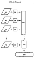
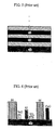
- FIGS.1-3 describe the known simultaneous deposition technique.
- FIG.1 shows a flow-chart of the process
- FIGS.2 and 3 give a cross section of the substrate and the deposited material during (FIG.2) and after (FIG.3) the deposition step.
- the base materials in this case Ba, Dy, and Cu, are evaporated from one or several sources 11, 12, 13, oxidized (OX) by the oxygen atoms or molecules in the deposition chamber, and deposited simultaneously in the deposition stage of the process (DEP) onto a substrate 20.
- the deposition step ends when the desired thickness of the film (FT) is reached.
- the cross section (FIG. 2) reveals that besides the deposition of the oxidized base materials BaO, Dy 2 O 3 , and CuO, already a growth of the desired "1:2:3"-unit cell of the superconductor 24 (DyBa 2 Cu 3 O 7 ) takes place at favoured positions. At less favoured places, impurities 25 are found. These impurities are often other compounds of the base materials than the desired superconducting compound 24, which also grow during the deposition step. The impurities 25, therefore, may be called non-stoichiometric compounds.
- FIG.3 which shows a cross section after the end of the deposition step (DEP)
- the impurities 25 may survive the formation of the superconducting material 24 together with the remainder of some base material (Dy 2 O 3 ), which may have stabilized itself on the substrate 20, resulting in an imperfect superconducting phase.
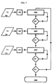
- FIGS.4-6 describe the known monolayer-by-monolayer deposition technique.
- FIG.4 shows a flow-chart of the process;
- FIGS.5 and 6 give a cross section of the substrate and the deposited material during the deposition step.
- a cross section after deposition like FIG.3 in case of the simultaneous deposition method is omitted as it shows no basic differences with regard to that figure.
- the general monolayer-by-monolayer process is characterized by successively depositing monolayers 51, 52, 53 of different base materials onto a substrate 20.
- the flow-chart denotes this deposition (DEP) without regarding the exact sequence of deposition for the sake of shortness.
- the sources 41, 42, 43 contribute in temporal order monolayers to the deposition process (DEP).
- the base material is oxidized (OX) during deposition by the oxygen present in the deposition chamber.
- the sequence of the monolayers 51,52,53 is chosen in accordance with the sequence of the atomic layers within the unit cell of the desired superconductor.
- the deposition procedure (DEP) is terminated when the intended number of monolayers 51, 52, 53 has been deposited.
- monolayers of BaO, CuO, BaO, CuO, Y 2 O 3 , CuO, BaO, CuO, and BaO are deposited in that sequence.
- FIGS.5 and 6 show intermediate states during the deposition step (DEP) with FIG.6 showing the state immediately following the deposition of the first Y 2 O 3 monolayer 52, i.e. following FIG.5. In fact, both states can hardly be separated and are presented by two figures primarily for the sake of clarity.
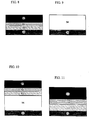
- FIGS.8 and 11 each show one period of deposited layers and FIG.9 shows the layers of FIG.8 after complete crystallization, i.e. when the substrate is covered by one layer of the superconducting compound with a height of one unit cell.
- Figure 10 shows the layer of the superconducting material, onto which the next period of layers is deposited.
- FIGS.8 and 9 A definite distinction between the states illustrated by both figures is primarily made for sake of clarity and can hardly be made otherwise.
- the base materials (Ba, Dy, Cu) are provided by sources 71, 72, 73.
- the deposition chamber is provided with enough oxygen achieve an oxidization (OX) of the base materials.
- Each base material is deposited (DEP) and oxidized (OX) with a layer thickness (LT) according to the stoichiometric ratio of the compound.
- the deposition of one layer of each base material i.e. the deposition of one period, is repeated until the desired film thickness (FT) is reached.
- a layer 81 of a simpler material (BaO) than the desired compound By first depositing on the substrate 20 a layer 81 of a simpler material (BaO) than the desired compound, the question of the nucleation of the complex compound is reduced to the question of the nucleation of a layer of the simpler material.
- a simpler material may have either a smaller unit cell, a higher melting point, fewer impurity phases in its phase diagram, or a combination of these items.
- a higher melting point will in general allow a growth mechanism which is more two-dimensional at the indicated substrate temperature.
- DyBa 2 Cu 3 O 7 the growth of a first (buffer) layer 81 of BaO proceeds entirely differently than the growth of a DyBa 2 Cu 3 O 7 block (as for example deposited by the simultaneous deposition, see above).
- BaO has a melting point of 1923°C , which is about 1000°C higher than the meting point of the superconductor, and grows therefore at 700°C close to a layer by layer manner. Since it has a relatively small unit cell and no impurities are found in its simple phase diagram, the eventually formed grains do not pose a serious problem upon joining together. As a consequence, the deposition of BaO as a buffer layer 81 composed of two BaO monolayers leaves a continuous and smooth film on the substrate. In the case of a SrTiO 3 substrate 20, the BaO film will grow epitaxially. The subsequent deposition of the Dy 2 O 3 block layer 82, consisting of one monolayer, does not fundamentally change this picture since no intermediate impurity phase (e.g.
- Ba 2 DyO x composition is formed, as the diffusion between both layers is small. At this point, only two components necessary for the formation of one layer of DyBa 2 Cu 3 O 7 are supplied to the substrate. This is radically different from the other deposition techniques (e.g. FIG.2), where at this point half a layer of nucleated DyBa 2 Cu 3 O 7 material 24, dispersed in small grains with local impurities 25, is present. Finally, the last block layer 83 consisting of three monolayers of CuO is deposited. Only at this point can the phase formation of the desired compound 94 start, as the estimated vertical diffusion lengths at 700°C for Cu, Ba and Dy are 60, 2 and 0.2nm, respectively.
- a DyBa 2 Cu 3 O 7 layer 94 is formed with a roughness (smoothness) comparable to that of the first deposited block layer 81 (FIG.8) and with no inclusions of other phases.
- the process can be repeated and a new period of blocks (81, 82, 83) deposited after the completion of one layer of DyBa 2 Cu 3 O 7 94.
- a new period of blocks 81, 82, 83
- FIG.10 What has been described previously is exactly repeated during this next deposition period.
- These periods of layers 81, 82, 83 can be repeated as often as necessary, until the required thickness of the film is achieved.
- DyBa 2 Cu 3 O 7 94 the order of layers is kept for the second and the periods following, it may be necessary or advantageous to change this order to achieve, for example, a better matching with crystal lattice of the superconducting material, which now serves as substrate for the newly deposited layers.
- a layer 111 of BaO consisting of three monolayers
- a layer 112 of Dy 2 O 3 consisting of 1,5 monolayers
- a layer 113 of CuO consisting of 4,5 monolayers
- Dy, Ba, and Cu were evaporated from their effusion cells, oxidized and deposited on the substrate ( SrTiO 3 ).
- a quartzmicrobalance monitored the layer deposition and was used to control the shutter at each effusion cell. The same microbalance was used to terminate deposition after reaching the final thickness of the film.
- the substrate temperature and the oxygen pressure were fixed to 700°C and 1.3 ⁇ 10 -4 Pa, respectively, throughout the entire process. The oxygen losses were balanced by a stream of 10 15 atoms per cm 2 and second into the deposition chamber, generated by a radio frequency plasma source.
- the period of block layers (81, 82, 83 in FIGS.8 and 10) consisted of the simple oxides BaO - Dy 2 O 3 - CuO, starting with BaO.
- the previously described growth behavior for this example was completely consistent with the RHEED data measured during the deposition of the blocks.
- the 'birth' of a DyBa 2 Cu 3 O 7 layer 94 (FIG.9) was observed by the appearance of strong streaks.
- Evidence for the presented method was further provided by cross-section TEM (transmission electron microscopy) data, which showed the absence of inclusions over large domains (1000 nm) and a roughness which was limited to +/- 1 unit cell.
Landscapes
- Engineering & Computer Science (AREA)
- Chemical & Material Sciences (AREA)
- Ceramic Engineering (AREA)
- Manufacturing & Machinery (AREA)
- Superconductors And Manufacturing Methods Therefor (AREA)
- Superconductor Devices And Manufacturing Methods Thereof (AREA)
- Crystals, And After-Treatments Of Crystals (AREA)
- Physical Vapour Deposition (AREA)
Claims (9)
- Procédé de fabrication d'un film mince d'un composé solide, de préférence d'un supraconducteur à Tc élevé, à partir d'une pluralité de matériaux de base par le dépôt multicouche périodique sur un substrat avec le rapport d'épaisseur de couche à l'intérieur de chaque période étant sélectionné en conformité avec le rapport stoechiométrique du composé, dans lequel chaque matériau de base est déposé comme une seule couche du bloc (81, 82, 83) à l'intérieur de chaque période, l'épaisseur de la couche du bloc la plus épaisse (83) à l'intérieur de chaque période est sélectionnée dans un intervalle entre 2 et 20 monocouches, de préférence entre 2 et 10 monocouches, le dépôt des couches du bloc (81, 82, 83) et la cristallisation du composé (94) sont réalisées approximativement à la même température et la cristallisation du composé (94) est réalisée avant le dépôt de la période suivante des couches du bloc (81, 82, 83).
- Procédé selon la revendication 1, dans lequel le nombre des différentes couches du bloc (81, 82, 83) dans une période de dépôt est égal à trois ou supérieur à trois.
- Procédé selon l'une quelconque des revendications précédentes, dans lequel deux desdits matériaux de base sont combinés afin de former un composé binaire avant d'être déposé comme une desdites couches du bloc.
- Procédé selon l'une quelconque des revendications précédentes, dans lequel le matériau de base qui croît épitaxialement sur le substrat (20) ou qui présente la cellule unitaire la plus petite est choisi comme couche de départ (81) du bloc.
- Procédé selon l'une quelconque des revendications précédentes, dans lequel le matériau de base ayant la longueur de diffusion la plus grande est déposé comme la dernière couche du bloc (83) dans la période de dépôt.
- Procédé selon l'une quelconque des revendications précédentes, dans lequel l'ordre du dépôt des couches du bloc (81, 82, 83) est changé à l'intérieur des périodes de dépôt ultérieures.
- Procédé selon l'une quelconque des revendications précédentes, dans lequel les matériaux de base sont sélectionnés à partir d'un groupe qui est constitué des métaux du groupe Ib-, IIa-, IIIa, des lanthanides, comprenant La et Y, du potassium, du plomb et/ou leurs oxydes et de l'oxygène.
- Procédé selon l'une quelconque des revendications précédentes, dans lequel lesdites couches du bloc (81, 82, 83) sont déposées par un procédé sélectionné à partir d'un groupe qui est constitué de l'épitaxie par faisceaux moléculaires (MBE), de la pulvérisation, de l'ablation par laser et du dépôt chimique en phase vapeur de métaux organiques (MOCVD).
- Utilisation d'un procédé selon l'une quelconque des revendications précédentes afin de fabriquer un composé ayant une cellule unitaire avec au moins un axe dépassant 1 nm.
Priority Applications (4)
| Application Number | Priority Date | Filing Date | Title |
|---|---|---|---|
| DE69219467T DE69219467T2 (de) | 1992-09-11 | 1992-09-11 | Verfahren zum Herstellen dünner Schichten durch Mehrlagen-Abscheidung |
| EP92810699A EP0586774B1 (fr) | 1992-09-11 | 1992-09-11 | Procédé de fabrication de films minces par déposition multicouche |
| JP5213821A JP2721785B2 (ja) | 1992-09-11 | 1993-08-30 | ペロブスカイト型多元化合物薄膜の周期的多層付着方法 |
| US08/120,984 US5648321A (en) | 1992-09-11 | 1993-09-13 | Process for manufacturing thin films by multi-layer deposition |
Applications Claiming Priority (1)
| Application Number | Priority Date | Filing Date | Title |
|---|---|---|---|
| EP92810699A EP0586774B1 (fr) | 1992-09-11 | 1992-09-11 | Procédé de fabrication de films minces par déposition multicouche |
Publications (2)
| Publication Number | Publication Date |
|---|---|
| EP0586774A1 EP0586774A1 (fr) | 1994-03-16 |
| EP0586774B1 true EP0586774B1 (fr) | 1997-05-02 |
Family
ID=8211986
Family Applications (1)
| Application Number | Title | Priority Date | Filing Date |
|---|---|---|---|
| EP92810699A Expired - Lifetime EP0586774B1 (fr) | 1992-09-11 | 1992-09-11 | Procédé de fabrication de films minces par déposition multicouche |
Country Status (4)
| Country | Link |
|---|---|
| US (1) | US5648321A (fr) |
| EP (1) | EP0586774B1 (fr) |
| JP (1) | JP2721785B2 (fr) |
| DE (1) | DE69219467T2 (fr) |
Families Citing this family (12)
| Publication number | Priority date | Publication date | Assignee | Title |
|---|---|---|---|---|
| US6022832A (en) * | 1997-09-23 | 2000-02-08 | American Superconductor Corporation | Low vacuum vapor process for producing superconductor articles with epitaxial layers |
| US6027564A (en) * | 1997-09-23 | 2000-02-22 | American Superconductor Corporation | Low vacuum vapor process for producing epitaxial layers |
| US6428635B1 (en) | 1997-10-01 | 2002-08-06 | American Superconductor Corporation | Substrates for superconductors |
| US6458223B1 (en) | 1997-10-01 | 2002-10-01 | American Superconductor Corporation | Alloy materials |
| US5972430A (en) * | 1997-11-26 | 1999-10-26 | Advanced Technology Materials, Inc. | Digital chemical vapor deposition (CVD) method for forming a multi-component oxide layer |
| US6110840A (en) * | 1998-02-17 | 2000-08-29 | Motorola, Inc. | Method of passivating the surface of a Si substrate |
| US6475311B1 (en) | 1999-03-31 | 2002-11-05 | American Superconductor Corporation | Alloy materials |
| US6613656B2 (en) * | 2001-02-13 | 2003-09-02 | Micron Technology, Inc. | Sequential pulse deposition |
| DE10296448T5 (de) * | 2001-03-20 | 2004-04-15 | Mattson Technology Inc., Fremont | Verfahren zum Abscheiden einer Schicht mit einer verhältnismässig hohen Dielektrizitätskonstante auf ein Substrat |
| WO2003089682A1 (fr) * | 2002-04-19 | 2003-10-30 | Mattson Technology, Inc. | Systeme conçu pour deposer un film sur un substrat au moyen d'un precurseur gazeux a faible pression de vapeur |
| US20040247787A1 (en) * | 2002-04-19 | 2004-12-09 | Mackie Neil M. | Effluent pressure control for use in a processing system |
| CN120719258B (zh) * | 2025-06-30 | 2026-01-23 | 甚磁科技(上海)有限公司 | 一种超导带材制备以及应力原位释放方法 |
Citations (1)
| Publication number | Priority date | Publication date | Assignee | Title |
|---|---|---|---|---|
| EP0426570A2 (fr) * | 1989-10-31 | 1991-05-08 | Sumitomo Electric Industries, Ltd. | Procédé et système pour préparation de film mince supraconducteur d'oxyde |
Family Cites Families (5)
| Publication number | Priority date | Publication date | Assignee | Title |
|---|---|---|---|---|
| EP0305292B1 (fr) * | 1987-08-24 | 1995-12-27 | Sumitomo Electric Industries Limited | Procédé pour la fabrication d'une couche mince d'oxyde supraconducteur composé |
| DE3851701T2 (de) * | 1988-06-03 | 1995-03-30 | Ibm | Verfahren zur Herstellung künstlicher Hochtemperatur-Supraleiter mit mehrschichtiger Struktur. |
| JPH03151231A (ja) * | 1989-10-13 | 1991-06-27 | Internatl Business Mach Corp <Ibm> | 多層ひずみ格子銅酸化物ペロブスカイト構造体 |
| JPH07108765B2 (ja) * | 1990-04-13 | 1995-11-22 | 東京工業大学長 | 分子線エピタキシー法による酸化物超伝導体薄膜の製造方法 |
| JPH04292419A (ja) * | 1991-03-18 | 1992-10-16 | Fujitsu Ltd | 酸化物超伝導体薄膜の形成方法 |
-
1992
- 1992-09-11 EP EP92810699A patent/EP0586774B1/fr not_active Expired - Lifetime
- 1992-09-11 DE DE69219467T patent/DE69219467T2/de not_active Expired - Fee Related
-
1993
- 1993-08-30 JP JP5213821A patent/JP2721785B2/ja not_active Expired - Fee Related
- 1993-09-13 US US08/120,984 patent/US5648321A/en not_active Expired - Fee Related
Patent Citations (1)
| Publication number | Priority date | Publication date | Assignee | Title |
|---|---|---|---|---|
| EP0426570A2 (fr) * | 1989-10-31 | 1991-05-08 | Sumitomo Electric Industries, Ltd. | Procédé et système pour préparation de film mince supraconducteur d'oxyde |
Non-Patent Citations (2)
| Title |
|---|
| "Growth of La-Ca-Mn-O films by ozone assisted molecular beam epotaxy" by Achutharaman et al. in Applied Physics Letters 67 (7), 14 August 1995, pp 1019-1021. * |
| "Microstructure of YBa2Cu3O7-x thin films deposited by laser evaporation" by O. Eibl and B. Roas in Journal of Materials Research, Vol. 5, No. 11, Nov. 1990, pages 2620-2632. * |
Also Published As
| Publication number | Publication date |
|---|---|
| DE69219467D1 (de) | 1997-06-05 |
| JP2721785B2 (ja) | 1998-03-04 |
| US5648321A (en) | 1997-07-15 |
| DE69219467T2 (de) | 1997-10-23 |
| EP0586774A1 (fr) | 1994-03-16 |
| JPH06188469A (ja) | 1994-07-08 |
Similar Documents
| Publication | Publication Date | Title |
|---|---|---|
| US5372992A (en) | Superconducting thin film | |
| US5712227A (en) | Substrate having a superconductor layer | |
| EP0586774B1 (fr) | Procédé de fabrication de films minces par déposition multicouche | |
| US7364989B2 (en) | Strain control of epitaxial oxide films using virtual substrates | |
| EP0410868B1 (fr) | Film mince supraconducteur d'oxyde et procédé pour sa fabrication | |
| EP0635894B1 (fr) | Structure laminé comportant une couche mince isolante et une couche mince en supraconducteur d'oxyde | |
| US7431868B2 (en) | Method of manufacturing a metal substrate for an oxide superconducting wire | |
| Wasa et al. | Thin film processing for high-Tc superconductors of the Bi-system | |
| US5292718A (en) | Process for preparing superconducting junction of oxide superconductor | |
| EP0620602B1 (fr) | Procédé de dépÔt d'un autre film mince sur un film mince en oxyde à structure cristalline perovskite | |
| JP2958455B1 (ja) | 酸化物薄膜の結晶成長方法 | |
| AU655731B2 (en) | Process for preparing superconducting junction of oxide superconductor | |
| CN1497614A (zh) | 高温超导层的制备方法 | |
| Haindl | Thin Film Growth of Fe-Based Superconductors | |
| US5260267A (en) | Method for forming a Bi-containing superconducting oxide film on a substrate with a buffer layer of Bi2 O3 | |
| Somekh et al. | The deposition of ceramic superconductors | |
| JP4809700B2 (ja) | Ybco系高温超電導体成膜用基材およびybco系高温超電導体膜の作製方法 | |
| JPH0586477A (ja) | ペロブスカイト型酸化物超薄膜の製造方法 | |
| JPH07206592A (ja) | 酸化物薄膜の製造方法 | |
| JP2541037B2 (ja) | 酸化物超電導薄膜合成方法 | |
| JPH11278996A (ja) | 酸化物薄膜の結晶成長方法 | |
| JPH0648738A (ja) | 超伝導積層薄膜およびその製造方法 | |
| JP3485601B2 (ja) | 超電導複合薄膜の製造方法 | |
| JPH03275504A (ja) | 酸化物超伝導体薄膜およびその製造方法 | |
| JPH06316415A (ja) | 酸化物超伝導体薄膜 |
Legal Events
| Date | Code | Title | Description |
|---|---|---|---|
| PUAI | Public reference made under article 153(3) epc to a published international application that has entered the european phase |
Free format text: ORIGINAL CODE: 0009012 |
|
| AK | Designated contracting states |
Kind code of ref document: A1 Designated state(s): DE FR GB |
|
| 17P | Request for examination filed |
Effective date: 19940718 |
|
| 17Q | First examination report despatched |
Effective date: 19950511 |
|
| GRAG | Despatch of communication of intention to grant |
Free format text: ORIGINAL CODE: EPIDOS AGRA |
|
| GRAH | Despatch of communication of intention to grant a patent |
Free format text: ORIGINAL CODE: EPIDOS IGRA |
|
| GRAH | Despatch of communication of intention to grant a patent |
Free format text: ORIGINAL CODE: EPIDOS IGRA |
|
| GRAA | (expected) grant |
Free format text: ORIGINAL CODE: 0009210 |
|
| AK | Designated contracting states |
Kind code of ref document: B1 Designated state(s): DE FR GB |
|
| PG25 | Lapsed in a contracting state [announced via postgrant information from national office to epo] |
Ref country code: FR Effective date: 19970502 |
|
| REF | Corresponds to: |
Ref document number: 69219467 Country of ref document: DE Date of ref document: 19970605 |
|
| PG25 | Lapsed in a contracting state [announced via postgrant information from national office to epo] |
Ref country code: GB Free format text: LAPSE BECAUSE OF NON-PAYMENT OF DUE FEES Effective date: 19970911 |
|
| EN | Fr: translation not filed | ||
| PLBE | No opposition filed within time limit |
Free format text: ORIGINAL CODE: 0009261 |
|
| 26N | No opposition filed | ||
| GBPC | Gb: european patent ceased through non-payment of renewal fee |
Effective date: 19970911 |
|
| PGFP | Annual fee paid to national office [announced via postgrant information from national office to epo] |
Ref country code: DE Payment date: 20030911 Year of fee payment: 12 |
|
| PG25 | Lapsed in a contracting state [announced via postgrant information from national office to epo] |
Ref country code: DE Free format text: LAPSE BECAUSE OF NON-PAYMENT OF DUE FEES Effective date: 20050401 |