EP0586965A2 - Méthode électrophotographique de formation d'images, appareil électrophotographique et appareillage électrophotographique - Google Patents
Méthode électrophotographique de formation d'images, appareil électrophotographique et appareillage électrophotographique Download PDFInfo
- Publication number
- EP0586965A2 EP0586965A2 EP93113580A EP93113580A EP0586965A2 EP 0586965 A2 EP0586965 A2 EP 0586965A2 EP 93113580 A EP93113580 A EP 93113580A EP 93113580 A EP93113580 A EP 93113580A EP 0586965 A2 EP0586965 A2 EP 0586965A2
- Authority
- EP
- European Patent Office
- Prior art keywords
- electrophotographic
- photosensitive member
- image
- oxytitanium phthalocyanine
- layer
- Prior art date
- Legal status (The legal status is an assumption and is not a legal conclusion. Google has not performed a legal analysis and makes no representation as to the accuracy of the status listed.)
- Withdrawn
Links
Images





Classifications
-
- G—PHYSICS
- G03—PHOTOGRAPHY; CINEMATOGRAPHY; ANALOGOUS TECHNIQUES USING WAVES OTHER THAN OPTICAL WAVES; ELECTROGRAPHY; HOLOGRAPHY
- G03G—ELECTROGRAPHY; ELECTROPHOTOGRAPHY; MAGNETOGRAPHY
- G03G5/00—Recording-members for original recording by exposure, e.g. to light, to heat or to electrons; Manufacture thereof; Selection of materials therefor
- G03G5/02—Charge-receiving layers
- G03G5/04—Photoconductive layers; Charge-generation layers or charge-transporting layers; Additives therefor; Binders therefor
- G03G5/06—Photoconductive layers; Charge-generation layers or charge-transporting layers; Additives therefor; Binders therefor characterised by the photoconductive material being organic
- G03G5/0664—Dyes
- G03G5/0696—Phthalocyanines
-
- G—PHYSICS
- G03—PHOTOGRAPHY; CINEMATOGRAPHY; ANALOGOUS TECHNIQUES USING WAVES OTHER THAN OPTICAL WAVES; ELECTROGRAPHY; HOLOGRAPHY
- G03G—ELECTROGRAPHY; ELECTROPHOTOGRAPHY; MAGNETOGRAPHY
- G03G13/00—Electrographic processes using a charge pattern
- G03G13/02—Sensitising, i.e. laying-down a uniform charge
- G03G13/025—Sensitising, i.e. laying-down a uniform charge by contact, friction or induction
Definitions
- the present invention relates to an electrophotographic image-forming method utilizing direct charging, and an electrophotographic apparatus and a unit therefor employing the method.
- inorganic photoconductive materials such as selenium, cadmium sulfide, zinc oxide, and the like are used as a photoconductive material for electrophotographic photosensitive members.
- organic photoconductive materials such as polyvinylcarbazoles, oxadiazoles, phthalocyanines, and the like have low sensitivity, although they have advantage of non-pollution and high productivity in comparison with the inorganic photoconductive materials. Therefore, several sensitization methods have been reported for the organic photoconductive materials.
- One effective sensitization method is use of a function-separation type photosensitive member which has a charge-generating layer and a charge-transporting layer in lamination.
- oxytitanium phthalocyanine used as a charge-generating substance of a photosensitive member tends to deteriorate on repeated use to exhibit a lower dark-area potential. Consequently, during repeated use, the photosensitive member tends to give lower quality images or to give image defects such as white dots (failure of toner transfer) and black dots (undesired excessive toner transfer). Especially at high temperatures and high humidities, the image defects are liable to increase.
- the present invention intends also to provide an electrophotographic apparatus and an electrophotographic apparatus unit employing the method.
- the electrophotographic image-forming method of the present invention comprises a charging step of charging an electrophotographic photosensitive member containing oxytitanium phthalocyanine in the photosensitive layer thereof by a direct charging method; an image-exposing step of exposing the photosensitive member having been charged to a light image to form an electrostatic latent image; and a developing step of developing the electrostatic latent image formed on the electrophotographic photosensitive member.
- the electrophotographic apparatus of the present invention comprises an electrophotographic photosensitive member having a photosensitive member containing oxytitanium phthalocyanine therein; a direct charging member for charging the electrophotographic photosensitive member by contact; an image-exposing means for exposing the charged electrophotographic photosensitive member to light in an image to form an electrostatic latent image; and a developing means for developing the formed electrostatic latent image on the electrophotographic photosensitive member.
- Fig. 1 is a front view of an example of the electrophotographic apparatus of the present invention.
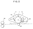
- Fig. 2 is a front view of another example of the electrophotographic apparatus of the present invention.
- Fig. 3 is a front view of still another example of the electrophotographic apparatus of the present invention.
- Fig. 4 is a front view of an example of the direct charging member employed in the electrophotographic apparatus of the present invention.
- Fig. 5 is a cross-sectional view of the side of the direct charging member shown in Fig. 4.
- Fig. 6 is a front view of another example of the direct charging member employed in the electrophotographic apparatus of the present invention.
- Fig. 7 is a front view of still another example of the direct charging member employed in the electrophotographic apparatus of the present invention.
- Fig. 8 is a front view of a further example of the direct charging member employed in the electrophotographic apparatus of the present invention.
- Fig. 9 is a cross-sectional view of a side of the direct charging member shown in Fig. 8.
- Fig. 10 is a front view of a further example of the electrophotographic apparatus of the present invention.
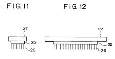
- Fig. 11 is a front view of a further example of the direct charging member employed in the electrophotographic apparatus of the present invention.
- Fig. 12 is a side view of the direct charging member shown in Fig. 11.
- Fig. 13 is a front view of still further example of the electrophotographic apparatus of the present invention.
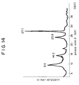
- Fig. 14 is an X-ray diffraction pattern of an example of oxytitanium phthalocyanine used in the present invention.
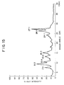
- Fig. 15 is an X-ray diffraction pattern of another example of oxytitanium phthalocyanine used in the present invention.
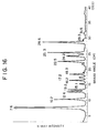
- Fig. 16 is an X-ray diffraction pattern of a still another example of oxytitanium phthalocyanine used in the present invention.
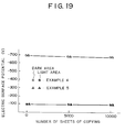
- Fig. 18 is a graph showing the results of the durability test of Comparative Examples 2 to 4.
- the direct charging is conducted as below.
- a drum-shaped electrophotographic photosensitive member 12 rotates in the arrow direction A .
- a direct charging member 1 to which DC voltage is applied is brought into contact with the peripheral surface of the photosensitive member 12, thereby the photosensitive member 12 is charged positively or negatively by the direct charging member 1.
- the DC voltage applied to the direct charging member is preferably in the range of from -2000 V to +2000 V.
- an AC voltage may be superposed to apply a pulse voltage to the direct charging member 1.
- the AC voltage superposed on the DC voltage is preferably not more than 4000 V between the peak voltages.
- the intended voltage may be applied instantaneously to the direct charging member 1, or gradually thereto by raising the voltage from a low level to the intended level in order to protect the photosensitive member.
- the direct charging member 1 may be rotated either in the same direction as that of the photosensitive member 12 or in the reverse direction, or may be not rotated to slide the peripheral surface of the photosensitive member.
- the direct charging member 1 may have simultaneously a function of cleaning a remaining toner on the photosensitive member 12. In this case, the cleaning means 10 need not be provided.
- the charged photosensitive member 12 is exposed to image exposure light 6 (e.g., slit exposure, laser beam-scanning exposure, etc.) with an image-exposure means (not shown in the drawing), whereby an electrostatic latent image is successively formed on the peripheral surface in accordance with the exposed image.
- image exposure light 6 e.g., slit exposure, laser beam-scanning exposure, etc.
- image-exposure means not shown in the drawing
- the formed electrostatic latent image is developed with a toner by a developing means 7.
- the developed toner image is successively transferred by a transfer-charging means 8 onto a surface of a recording medium 9 which is fed between the photosensitive member 12 and the transfer-charging means 8 synchronously with the rotation of the photosensitive member 12 from a recording medium feeder (not shown in the drawing).
- the recording medium 9 which has received the transferred image is separated from the photosensitive member surface, and introduced to an image-fixing means (not shown in the drawing) for fixation of the image and sent out from the
- the surface of the photosensitive member 12, after the image transfer, is cleaned with a cleaning means 10 to remove any remaining un-transferred toner, and is treated for charge elimination by pre-exposure 11 for repeated use for image formation.
- two or more of the constitutional elements may be integrated into one device unit, which may be made demountable from the main body of the apparatus.
- a photosensitive member 12, a direct charging member 1, and a developing means 7 at least are enclosed in a container 20 to construct an electrophotographic device unit, and this device unit is made demountable by use of a guiding means such as a rail in the main body of the apparatus.
- the cleaning means 10 may be provided in the container 20, or not. Otherwise, as shown in Fig.
- a photosensitive member 12, and a direct charging member 1 at least are enclosed in a first container 21 to construct a first electrophotographic device unit, and a developing means 7 at least is enclosed in a second container 22 to construct a second electrophotographic apparatus unit: the first and second apparatus units may be made demountable from the main body of the apparatus.
- the cleaning means 10 may be provided in the container 21, or not.
- a direct charging member 23 is used as the transfer-charging means. This direct charging member 23 may be used of the same construction as the direct charging member 1.
- DC voltage is applied in the range of preferably from 400 V to 1000 V.
- the numeral 24 denotes a fixing means.
- the photosensitive member 12 comprises a photosensitive layer and a support therefor.
- the photosensitive layer may be formed by lamination of a charge-generating layer and a charge-transporting layer.
- the charge-generating layer contains a charge-generating substance which generates electric charge on light exposure, and the charge-transporting layer contains a charge-transporting substance which transport electric charge.
- the charge-generating substance is oxytitanium phthalocyanine.
- the charge-generating layer and the charge-transporting layer may be formed on a support in this order or in the reverse order.
- the charge-generating layer may be formed by vapor-depositing oxytitanium phthalocyanine as the charge-generating substance on a support, or by dispersing oxytitanium phthalocyanine with or without a binder to form a coating liquid and applying the dispersion on a support.
- the oxytitanium phthalocyanine is preferably the one which has the highest peak at a diffraction angle (20 ⁇ 0.2°) of 27.1° in CuK ⁇ characteristic X-ray diffraction: particularly preferred are the one having the peaks at least at 9.0°, 14.2°, 23.9°, and 27.1°, and the one having the peaks at least at 9.2° and 27.1°. Further, oxytitanium phthalocyanine having the peaks of the diffraction angle (2 ⁇ ⁇ 0.2°) at least at 7.6° and 28.6° is suitably used.
- the X-ray diffraction was measured by use of CuK ⁇ line under the conditions below:
- the charge-generating layer has a thickness ranging preferably from 0.01 to 15 ⁇ m, more preferably from 0.05 to 5 ⁇ m.
- the ratio by weight of the charge-generating substance and the binder is preferably in the range of from 10 : 1 to 1 : 20.
- the organic solvent for coating application of the charge-generating layer is selected in consideration of the solubility and the dispersion stability of the used resin and the charge-generating substance, and includes alcohols, sulfoxides, ethers, esters, aliphatic halogenated hydrocarbons, and aromatic compounds.
- the charge-transporting layer may be formed by use of a solution of a charge-transporting substance and a binder having a film-forming property.
- the charge-transporting substance includes hydrazones, stilbenes, pyrazolines, oxazoles, thiazoles, triarylamines, and the like.
- the charge-transporting substance may be used singly or in combination of two or more thereof.
- the binder for the charge-transporting layer includes polyvinylbutyrals, polyesters, polycarbonates (polycarbonate Z, modified polycarbonates, etc.), nylons, polyimides, polyarylates, polyurethanes, styrene-butadiene copolymers, styrene-acrylic acid copolymers, styrene-acrylonitrile copolymers, and the like.
- the organic solvent of the application of the charge-transporting layer includes the same ones as used in application of the charge-generating layer.
- the thickness of the charge-transporting layer is in the range of preferably from 5 to 50 ⁇ m, more preferably from 8 to 20 ⁇ m.
- the ratio by weight of the charge-transporting substance and the binder is preferably in the range of from 5 : 1 to 1 : 5, more preferably from 3 : 1 to 1 : 3.
- the coating of the charge-generating layer and the charge-transporting layer may be conducted by dip coating, spray coating, Meyer bar coating, blade coating, or a like coating method.
- the photosensitive layer may be of a one-layer structure: the layer containing both a charge-generating substance and a charge-transporting substance without separating the charge-generating layer and the charge transporting-layer.
- the support may be made of an electroconductive material such as aluminum, aluminum alloys, stainless steel, and the like.
- a sheet of a plastic, paper, or a metal on which an electroconductive surface layer is formed may also be useful as the support.
- the electroconductive surface layer includes vacuum vapor deposition films of aluminum, aluminum alloys, indium oxide-tin oxide alloys, and the like; and coating films formed by application of a mixture of an electroconductive particles (e.g., carbon black, particulate tin oxide, etc.) and a binder.
- the thickness of the electroconductive surface layer is preferably in the range of from 1 to 30 ⁇ m.
- a subbing layer may be provided which has a barrier function or an adhesion function, if necessary.
- the subbing layer may be formed from a material such as casein, polyvinyl alcohol, nitrocellulose, ethylene-acrylic acid copolymer, polyamide, modified polyamide, polyurethane, gelatin, aluminum oxide, and the like.
- the thickness of the subbing layer is preferably not more than 5 ⁇ m, more preferably in the range of from 0.5 to 3 ⁇ m.
- the subbing layer has preferably a resistivity of not less than 107 ⁇ cm.
- a protecting layer may be provided on the photosensitive layer, if necessary.
- the protecting layer may be formed by applying a solution of a resin in an organic solvent onto the photosensitive layer and drying it.
- the resin for the protecting layer includes polyvinylbutyrals, polyesters, polycarbonates (polycarbonate Z, modified polycarbonates, etc.), nylons, polyimides, polyarylates, polyurethanes, styrene-butadiene copolymers, styrene-acrylic acid copolymers, styrene-acrylonitrile copolymers, and the like.
- the thickness of the protecting layer is preferably in the range of from 0.05 to 20 ⁇ m.
- the protecting layer may contain a UV-absorbing agent.
- the direct charging member 1 may be in any shape of a roller, a brush, a blade, a belt, a plate, etc.
- the direct charging member shown in Figs. 4 and 5 is in a shape of a roller, constructed of an electroconductive core material 2 in a bar shape, and around it an elastic layer 3, electroconductive layer 4, and resistance layer 5.
- the electroconductive core material 2 may be made of a metal such as iron, copper, and stainless steel, an electroconductive resin such as resins containing carbon dispersed therein, and resins having particulate metal dispersed therein.
- the core material may be in a bar shape or a plate shape.
- the elastic layer 3 has high elasticity and low hardness.
- the rubber hardness of the elastic layer is preferably not higher than 35°, more preferably not higher than 30°, still more preferably in the range of from 12° to 25° as measured by use of a JIS-A type tester (trade name: Teclock GS-706, made by Teclock Co.) according to JIS K-6301.
- the thickness of the elastic layer 3 is preferably not less than 1.5 mm, more preferably not less than 2 mm, still more preferably in the range of from 3 mm to 13 mm.
- the material of the elastic layer 3 includes rubbers and sponges such as chloroprene rubbers, isoprene rubbers, EPDM rubbers, polyurethane rubbers, epoxy rubbers, and butyl rubbers; thermoplastic elastomers such as styrene-butadiene thermoplastic elastomers, polyurethane type thermoplastic elastomers, polyester type thermoplastic elastomers, and ethylene-vinyl acetate type thermoplastic elastomers; and the like.
- the elastic layer 3 may contain an electroconductive particulate material to adjust its hardness.
- the electroconductive layer 4 has a high electroconductivity: a volume resistivity of preferably not higher than 107 ⁇ cm, more preferably not higher than 106 ⁇ cm, still more preferably in the range of from 10 ⁇ 2 ⁇ cm to 106 ⁇ cm.
- the thickness of the electroconductive layer 4 is desirably thinner in order to give the effect of the softness of the underlying elastic layer to the upper resistance layer 5, being preferably not more than 3 mm, more preferably not more than 2 mm, still more preferably in the range of from 20 ⁇ m to 1 mm.
- the electroconductive layer 4 may be made from a metal vapor deposition film, a resin having a particulate electroconductive material dispersed therein, an electroconductive resin, or the like.
- the metal for the metal vapor deposition film includes aluminum, indium, nickel, copper, and iron.
- the particulate electroconductive material to be dispersed in the resin includes particles of carbon, aluminum, nickel, titanium oxide, etc., and the resin in which the particulate electroconductive material is dispersed includes urethane resins, polyester resins, vinyl acetate-vinyl chloride copolymers, polymethyl methacrylate, etc.
- the electroconductive resin includes polymethyl methacrylate resins having quaternary ammonium groups, polyvinylanilines, polyvinylpyrroles, polydiacetylenes, polyethyleneimines, etc. Of these, the resins having a particulate electroconductive material are preferred in view of the control of electroconductivity.
- the insulating resin for dispersing the particulate electroconductive material includes urethane resins, polyester resins, vinyl acetate-vinyl chloride copolymers, polymethacrylic acid, etc., and the particulate electroconductive material dispersed in the resin includes electroconductive particles of carbon, aluminum, indium oxide, titanium oxide, etc.
- the resistance of the insulating resin is adjusted by dispersing the electroconductive particulate material in a small amount.
- the thickness of the resistance layer 5 is preferably from 1 ⁇ m to 500 ⁇ m, more preferably from 50 ⁇ m to 200 ⁇ m in view of chargeability.
- the inner resistance layer preferably has a volume resistivity of from 10 to 106 times, preferably from 102 to 105 times as high as that of the electroconductive layer 4.
- the resistivity of the inner resistance layer is in the range of preferably from 106 ⁇ cm to 1012 ⁇ cm, more preferably from 107 ⁇ cm to 1011 ⁇ cm.
- the thickness of the inner resistance layer is in the range of preferably from 1 ⁇ m to 450 ⁇ m, more preferably from 50 ⁇ m to 200 ⁇ m.
- the material for the inner resistance layer includes resins such as ethylcellulose , nitrocellulose, methoxymethylated nylon, ethoxymethylated nylon, copolymer nylon, polyvinylpyrrolidone, casein, etc., and mixtures thereof; semiconductive resins composed of the aforementioned resin and a small amount of electroconductive particles dispersed therein; insulating resins having dispersed electroconductive particles such as urethane resins, polyester resins, vinyl acetate-vinyl chloride copolymer resins, polymethacrylate resins, and the like containing a particulate electroconductive material such as carbon, aluminum, indium oxide, titanium oxide, etc.
- resins such as ethylcellulose , nitrocellulose, methoxymethylated nylon, ethoxymethylated nylon, copolymer nylon, polyvinylpyrrolidone, casein, etc., and mixtures thereof; semiconductive resins composed of the aforementioned resin and a small amount of electroconductive particles dispersed there
- the resin which is used for forming the inner resistance layer has a tensile modulus of preferably not higher than 200 kgf/mm2, more preferably from 50 kgf/mm2 to 150 kgf/mm2 in view of the flexibility.
- the rubber which is used for forming the inner resistance layer has a rubber hardness of preferably not higher than 35°, more preferably from 10° to 30° measured as mentioned before.
- the thickness of the surface resistance layer is preferably lower than that of the inner resistance layer so as not to impair the flexibility of the underlying inner resistance layer, and is in the range of preferably from 0.1 ⁇ m to 50 ⁇ m, more preferably from 1 ⁇ m to 30 ⁇ m.
- the surface resistance layer may be made of a material selected from the above-mentioned semiconductive resins and the above-mentioned insulating resin containing the electroconductive particles dispersed therein.
- the direct charging member 1 may further comprise additional layer or layers such as an adhesion layer to improve adhesiveness of respective layers.
- a metal bar is used as the core material 2.
- a material for the elastic layer is formed into the elastic layer 3 on this metal bar by melt molding, cast molding, dip coating, or spray coating.
- a material for the electroconductive layer is formed into the electroconductive layer 4 on the elastic layer 3 by melt molding, cast molding, dip coating, or spray coating.
- a material for the resistance layer 5 is formed into the resistance layer 5 on the electroconductive layer 4 by dip coating, spray coating, gravure coating, or the like.
- the direct charging means shown in Fig. 6 is in a shape of a plate, which has no core material 2.
- This direct charging means is prepared by forming, on an elastic layer 3, an electroconductive layer 4 and a resistance layer 5.
- the direct charging means shown in Fig. 7 is in a shape of a blade.
- a metal plate is used as the electroconductive core material 2.
- An elastic layer 3 and a resistance layer 5 is formed thereon.
- the direct charging member shown in Fig. 7 has an elastic layer 3 which has electroconductivity, therefore having no electroconductive layer 4.
- the direct charging means shown in Figs. 8 and 9 is in a shape of a brush, having electroconductive fibers 26 provided radially.
- the electroconductive fibers 26 are attached radially on the periphery of an electroconductive core material 2 by the aid of an adhesive layer 25.
- the electroconductive fiber 26 may be made of a material selected from the above-mentioned resin containing the electroconductive particles dispersed therein and electroconductive resins. Carbon fiber is useful as the electroconductive fiber 26.
- the carbon fiber which is produced by partial carbonization of polyacrylonitrile fiber by treatment at a temperature of from about 500°C to about 750°C is preferably used as the electroconductive fiber 26.
- This type of carbon fiber has resistivity of from about 102 to 105 ⁇ cm , and produced commercially by Celanese Co. with the trade name of CELECT 675.
- a resistance layer may be provided for controlling the resistance thereof.
- This resistance layer may be made from the same material as the ones of the resistance layer 5 as mentioned by reference to Figs. 4 to 6.
- the thickness of the resistance layer provided on the electroconductive fiber 26 is preferably in the range of from 0.01 ⁇ m to 5.0 ⁇ m, more preferably from 0.5 ⁇ m to 2.0 ⁇ m.
- a process for producing the electroconductive fiber 26 is described below as an example.
- Carbon disulfide is added to alkali-cellulose to form sodium cellulose xanthate.
- electroconductive powdery carbon is added and dispersed. This dispersion is discharged through a spinning nozzle into aqueous solution of a mixture of sulfuric acid and sodium sulfate to coagulate it in a fiber shape by applying an appropriate tension to form electroconductive cellulose fiber.
- a resistance layer is provided on the surface of the electroconductive fiber, a material for the resistance layer is dissolved in a solvent, and the solution is applied on the fiber and is dried to form electroconductive fiber having a resistance layer.
- the electrophotographic apparatus shown in Fig. 10 employs a brush-shaped direct charging member 100 in place of the roller-shaped direct charging member 1 in the electrophotographic apparatus shown in Fig. 1.
- the direct charging member shown in Figs. 11 and 12 constituted of a metal plate 27 and electroconductive fiber 26 provided on a face thereof with interposition of an adhesion layer 25.
- the electrophotographic apparatus shown in Fig. 13 is different from the one shown in Fig. 2 in that a brush-shaped direct charging member 101 shown in Figs. 11 and 12 is used in place of the roller-shaped direct charging member 1 in Fig. 2 and a brush-shaped direct charging member 102 is used in place of the roller-shaped direct charging member 23 in Fig. 2 as the transfer-charging means.
- the electroconductive fiber 26 is preferably provided on the surface of the adhesion layer 25 at a density of preferably from 1 ⁇ 104 to 5 ⁇ 106 fibers/cm2.
- the present invention enables maintenance of constant dark-area potential and light-area potential of an electrophotographic photosensitive member even under the environmental conditions of high temperature and high humidity, giving images of high quality without image defect in continuous copying.
- the direct charging member shown in Fig. 4 was prepared.
- An iron bar of 3 mm in diameter and 240 mm in length was used as the electroconductive core material.
- a chloroprene rubber layer of 3.5 mm thick and 220 mm wide was formed as the elastic layer by melt molding.
- the chloroprene rubber had a hardness of 15° according to JIS K-6301 as measured with a JIS-A type tester (Teclock GS-706, a rubber hardness tester made by Teclock Co.).
- an electroconductive polyurethane paint (trade name: Shintron, made by Shinto Paint Co., Ltd.) containing carbon particles was applied by dip coating, and was dried to form an electroconductive layer of 1 mm thick.
- electroconductive carbon (trade name: KETJEN Black, made by Lion Corporation), 19 parts of methoxymethylated nylon, 0.01 part of a surfactant (trade name: Sorbitol, made by Ajinomoto Co., Ltd.), and 80 parts of methanol were mixed and dispersed by ball mill to prepare a coating liquid. On the inner resistance layer, was applied the coating liquid by spray coating, and the applied matter was dried to form a surface resistance layer of 10 ⁇ m thick. Thus the direct charging member shown in Fig. 4 was prepared.
- the volume resistivity of the electroconductive elastic layer was measured in the same manner as in Production Example 1, and was found to be 4 ⁇ 106 ⁇ cm.
- an electroconductive core material made of iron bar of 3 mm in diameter and 240 mm in length was applied a liquid dispersion prepared by dispersing 10 parts of electroconductive carbon (trade name: Conductex C-975, made by Columbian Carbon Co.) and 90 parts of polyvinylbutyral (trade name: Eslec BLS, made by Sekisui Chemical Co., Ltd.) in 300 parts of methyl ethyl ketone to obtain an adhesion layer of 1 mm thick.
- electroconductive carbon trade name: Conductex C-975, made by Columbian Carbon Co.
- polyvinylbutyral trade name: Eslec BLS, made by Sekisui Chemical Co., Ltd.
- the electroconductive fiber employed was the one prepared as mentioned above, having a diameter of 10 ⁇ m and a volume resistivity of 5 ⁇ 105 ⁇ cm. This fiber was cut in a length of 5 mm, and was attached on the adhesion layer at a density of 1 ⁇ 105 fibers/cm2. Then the adhesion layer was heated and dried to obtain the direct charging member as shown in Fig. 8.
- a direct charging member as shown in Fig. 11 was prepared.
- Crystalline oxytitanium phthalocyanine was prepared as below.
- This crystalline matter was dissolved in 150 parts of concentrated sulfuric acid, and the solution was added dropwise into 1500 parts of deionized water at 20°C.
- the deposited matter was collected by filtration, and the matter was washed with water to obtain non-crystalline oxytitanium phthalocyanine.
- 4.0 parts of the non-crystalline oxytitanium phthalocyanine thus obtained was added to 100 parts of methanol, and stirred in a suspension state at room temperature (22°C) for 8 hours.
- the suspension was filtered, and the collected solid matter was dried to obtain low crystalline oxytitanium phthalocyanine.
- 40 parts of n-butyl ether was added and the mixture was subjected to milling treatment with glass beads of 1 mm diameter at room temperature (22°C) for 20 hours.
- Crystalline oxytitanium phthalocyanine was prepared as below.
- This crystalline matter was dissolved in 30 parts of concentrated sulfuric acid, and the solution was added dropwise into 300 parts of deionized water at 20°C.
- the deposited matter was collected by filtration to obtain non-crystalline oxytitanium phthalocyanine.
- 15 parts of sodium chloride and 7 parts of diethylene glycol were added, and the mixture was subjected to milling treatment at 80°C for 60 hours by means of an automatic mortar.
- the treated matter was washed with water sufficiently to remove sodium chloride and diethylene glycol therefrom completely, and was dried at a reduced pressure.
- the dried matter was treated with 200 parts of cyclohexanone for 30 minutes by mean of a sand mill by use of glass beads of 1 mm diameter to obtain 1.8 parts of crystalline oxytitanium phthalocyanine.
- the X-ray diffraction pattern thereof is shown in Fig. 15.
- Oxytitanium phthalocyanine was prepared according to the method disclosed in Japanese Patent Application Laid-Open No. 61-239248 (USP 4,728,592). The X-ray diffraction pattern of the resulting oxytitanium phthalocyanine is shown in Fig. 16.
- a coating liquid for an electroconductive surface layer was prepared by dispersing 50 parts of titanium oxide coated with tin oxide containing 10% antimony oxide, 25 parts of a resol type phenol resin, 20 parts of methylcellosolve, 5 parts of methanol, and 0.002 parts of silicone oil (polydimethylsiloxane-polyoxyalkylene copolymer, average molecular weight: 3,000) by means of a sand mill with glass beads of 1 mm diameter for 2 hours.
- silicone oil polydimethylsiloxane-polyoxyalkylene copolymer, average molecular weight: 3,000
- the above coating liquid was applied by dip coating, and was dried at 140°C for 30 minutes to form a electroconductive surface layer of 20 ⁇ m thick.
- a subbing layer was formed in a thickness of 1 ⁇ m by applying and drying a solution of 5 parts of an N-methoxymethylated nylon resin in a mixed solvent of 70 parts of methanol and 25 parts of butanol by dip coating.
- An electrophotographic photosensitive member was prepared in the same manner as in Example 1 except that the oxytitanium phthalocyanine was displaced by the one obtained in Production Example 6.
- An electrophotographic photosensitive member was prepared in the same manner as in Example 1 except that the oxytitanium phthalocyanine was displaced by the one obtained in Production Example 7.
- An electrophotographic photosensitive member was prepared in the same manner as in Example 1 except that the oxytitanium phthalocyanine was displaced by ⁇ type copper phthalocyanine of the same crystal shape as the one disclosed in Japanese Patent Application Laid-Open No. 50-38543.
- the electrophotographic photosensitive members prepared in Examples 1, 2, and 3, and Comparative Example 1 were respectively mounted on an electrophotographic apparatus shown in Fig. 1, and were tested for durability.
- the electrophotographic apparatus employed was a laser beam printer LBP-SX made by Canon K.K. modified to have a direct charging system, and uses the direct charging member 1 prepared in Production Example 1.
- DC voltage between peaks of -720 V and AC voltage of 1500 V were applied in superposition, and the dark-area potential was set at -700 V.
- This photosensitive member was subjected to imagewise exposure of laser light of an wavelength of 780 nm, and the light-area potential was set at -100 V.
- the respective photosensitive member was tested for durability by conducting continuous recording on 10,000 sheets of recording paper at the above potentials under environmental conditions of temperature of 30°C and humidity of 90 %.
- the durability was evaluated by the change of the dark-area potential, the change of the light-area potential, and the quality of the formed image.
- the changes of the dark-area potential and the changes of the light-area potential of the aforementioned four photosensitive member are shown in Fig. 17.
Landscapes
- Physics & Mathematics (AREA)
- General Physics & Mathematics (AREA)
- Photoreceptors In Electrophotography (AREA)
- Electrostatic Charge, Transfer And Separation In Electrography (AREA)
Applications Claiming Priority (4)
| Application Number | Priority Date | Filing Date | Title |
|---|---|---|---|
| JP251865/92 | 1992-08-28 | ||
| JP25186692 | 1992-08-28 | ||
| JP251866/92 | 1992-08-28 | ||
| JP25186592 | 1992-08-28 |
Publications (2)
| Publication Number | Publication Date |
|---|---|
| EP0586965A2 true EP0586965A2 (fr) | 1994-03-16 |
| EP0586965A3 EP0586965A3 (fr) | 1994-10-12 |
Family
ID=26540402
Family Applications (1)
| Application Number | Title | Priority Date | Filing Date |
|---|---|---|---|
| EP19930113580 Withdrawn EP0586965A3 (fr) | 1992-08-28 | 1993-08-25 | Méthode électrophotographique de formation d'images, appareil électrophotographique et appareillage électrophotographique. |
Country Status (1)
| Country | Link |
|---|---|
| EP (1) | EP0586965A3 (fr) |
Cited By (2)
| Publication number | Priority date | Publication date | Assignee | Title |
|---|---|---|---|---|
| EP0643339A1 (fr) * | 1993-09-09 | 1995-03-15 | Canon Kabushiki Kaisha | Procédé et appareil de formation d'images électrophotographique et unité de dispositif |
| EP0686878A1 (fr) * | 1994-06-10 | 1995-12-13 | Canon Kabushiki Kaisha | Elément photosensible électrophotographique, appareil électrophotographique le comprenant, ainsi qu'une unité de construction d'appareil électrophotographique |
Family Cites Families (3)
| Publication number | Priority date | Publication date | Assignee | Title |
|---|---|---|---|---|
| US3907559A (en) * | 1969-10-03 | 1975-09-23 | Xerox Corp | Imaging process employing friction charging in the presence of an electrically insulating developer liquid |
| US5008706A (en) * | 1988-10-31 | 1991-04-16 | Canon Kabushiki Kaisha | Electrophotographic apparatus |
| EP0428102B1 (fr) * | 1989-11-13 | 1996-09-25 | Canon Kabushiki Kaisha | Elément photosensible, appareil électrophotographique et procédé de formation d'images l'utilisant |
-
1993
- 1993-08-25 EP EP19930113580 patent/EP0586965A3/fr not_active Withdrawn
Cited By (4)
| Publication number | Priority date | Publication date | Assignee | Title |
|---|---|---|---|---|
| EP0643339A1 (fr) * | 1993-09-09 | 1995-03-15 | Canon Kabushiki Kaisha | Procédé et appareil de formation d'images électrophotographique et unité de dispositif |
| US5538826A (en) * | 1993-09-09 | 1996-07-23 | Canon Kabushiki Kaisha | Electrophotographic image forming method, apparatus and device unit |
| EP0686878A1 (fr) * | 1994-06-10 | 1995-12-13 | Canon Kabushiki Kaisha | Elément photosensible électrophotographique, appareil électrophotographique le comprenant, ainsi qu'une unité de construction d'appareil électrophotographique |
| US5595845A (en) * | 1994-06-10 | 1997-01-21 | Canon Kabushiki Kaisha | Electrophotographic photosensitive member, electrophotographic apparatus including same and electrophotographic apparatus unit |
Also Published As
| Publication number | Publication date |
|---|---|
| EP0586965A3 (fr) | 1994-10-12 |
Similar Documents
| Publication | Publication Date | Title |
|---|---|---|
| US5089851A (en) | Charging member | |
| JP2584873B2 (ja) | 電子写真装置 | |
| US9360779B2 (en) | Electrophotographic photoconductor, process cartridge, and electrophotographic apparatus | |
| US5538826A (en) | Electrophotographic image forming method, apparatus and device unit | |
| JP3186299B2 (ja) | 電子写真感光体 | |
| JP3560798B2 (ja) | 電子写真感光体およびそれを用いた画像形成装置 | |
| JPH10177269A (ja) | 電子写真装置及び画像形成方法 | |
| JP4045944B2 (ja) | 電子写真感光体、電子写真感光体の製造方法、プロセスカートリッジ及び電子写真装置 | |
| JP2894508B2 (ja) | 帯電用部材 | |
| JP2614316B2 (ja) | 帯電用部材及びこの帯電用部材を用いた電子写真装置 | |
| JPH10207085A (ja) | 電子写真感光体 | |
| JP2003262971A (ja) | 電子写真感光体の製造方法、電子写真感光体、プロセスカートリッジ及び電子写真装置 | |
| JP2765660B2 (ja) | 帯電用部材 | |
| JP3031967B2 (ja) | 帯電用部材 | |
| JP2966910B2 (ja) | 帯電用部材 | |
| JP2765662B2 (ja) | 帯電用部材 | |
| JP2002351107A (ja) | 電子写真感光体、それを用いた電子写真画像形成方法及び電子写真画像形成装置 | |
| JP2866451B2 (ja) | 帯電用部材 | |
| JP3240090B2 (ja) | 画像形成方法 | |
| JP2894510B2 (ja) | 帯電用部材 | |
| JP2866446B2 (ja) | 帯電用部材 | |
| JP2966896B2 (ja) | 帯電用部材 | |
| JPH06175383A (ja) | 電子写真画像形成方法、電子写真装置及び電子写真装置ユニット | |
| JP2894507B2 (ja) | 帯電用部材及びその製造方法 | |
| JP2894509B2 (ja) | 帯電用部材 |
Legal Events
| Date | Code | Title | Description |
|---|---|---|---|
| PUAI | Public reference made under article 153(3) epc to a published international application that has entered the european phase |
Free format text: ORIGINAL CODE: 0009012 |
|
| AK | Designated contracting states |
Kind code of ref document: A2 Designated state(s): DE ES FR GB IT |
|
| PUAL | Search report despatched |
Free format text: ORIGINAL CODE: 0009013 |
|
| AK | Designated contracting states |
Kind code of ref document: A3 Designated state(s): DE ES FR GB IT |
|
| 17P | Request for examination filed |
Effective date: 19950407 |
|
| 17Q | First examination report despatched |
Effective date: 19970710 |
|
| 18D | Application deemed to be withdrawn |
Effective date: 19980121 |