EP0588603B1 - Boítier pour système électronique scellé hermétiquement et procédé pour sa fabrication - Google Patents
Boítier pour système électronique scellé hermétiquement et procédé pour sa fabrication Download PDFInfo
- Publication number
- EP0588603B1 EP0588603B1 EP93307249A EP93307249A EP0588603B1 EP 0588603 B1 EP0588603 B1 EP 0588603B1 EP 93307249 A EP93307249 A EP 93307249A EP 93307249 A EP93307249 A EP 93307249A EP 0588603 B1 EP0588603 B1 EP 0588603B1
- Authority
- EP
- European Patent Office
- Prior art keywords
- layer
- barrier layer
- polymer
- support frame
- barrier
- Prior art date
- Legal status (The legal status is an assumption and is not a legal conclusion. Google has not performed a legal analysis and makes no representation as to the accuracy of the status listed.)
- Expired - Lifetime
Links
Images

Classifications
-
- H—ELECTRICITY
- H10—SEMICONDUCTOR DEVICES; ELECTRIC SOLID-STATE DEVICES NOT OTHERWISE PROVIDED FOR
- H10W—GENERIC PACKAGES, INTERCONNECTIONS, CONNECTORS OR OTHER CONSTRUCTIONAL DETAILS OF DEVICES COVERED BY CLASS H10
- H10W70/00—Package substrates; Interposers; Redistribution layers [RDL]
- H10W70/60—Insulating or insulated package substrates; Interposers; Redistribution layers
- H10W70/611—Insulating or insulated package substrates; Interposers; Redistribution layers for connecting multiple chips together
- H10W70/614—Insulating or insulated package substrates; Interposers; Redistribution layers for connecting multiple chips together the multiple chips being integrally enclosed
-
- H—ELECTRICITY
- H10—SEMICONDUCTOR DEVICES; ELECTRIC SOLID-STATE DEVICES NOT OTHERWISE PROVIDED FOR
- H10W—GENERIC PACKAGES, INTERCONNECTIONS, CONNECTORS OR OTHER CONSTRUCTIONAL DETAILS OF DEVICES COVERED BY CLASS H10
- H10W70/00—Package substrates; Interposers; Redistribution layers [RDL]
- H10W70/01—Manufacture or treatment
- H10W70/05—Manufacture or treatment of insulating or insulated package substrates, or of interposers, or of redistribution layers
- H10W70/093—Connecting or disconnecting other interconnections thereto or therefrom, e.g. connecting bond wires or bumps
-
- H—ELECTRICITY
- H10—SEMICONDUCTOR DEVICES; ELECTRIC SOLID-STATE DEVICES NOT OTHERWISE PROVIDED FOR
- H10W—GENERIC PACKAGES, INTERCONNECTIONS, CONNECTORS OR OTHER CONSTRUCTIONAL DETAILS OF DEVICES COVERED BY CLASS H10
- H10W70/00—Package substrates; Interposers; Redistribution layers [RDL]
- H10W70/60—Insulating or insulated package substrates; Interposers; Redistribution layers
-
- H—ELECTRICITY
- H10—SEMICONDUCTOR DEVICES; ELECTRIC SOLID-STATE DEVICES NOT OTHERWISE PROVIDED FOR
- H10W—GENERIC PACKAGES, INTERCONNECTIONS, CONNECTORS OR OTHER CONSTRUCTIONAL DETAILS OF DEVICES COVERED BY CLASS H10
- H10W70/00—Package substrates; Interposers; Redistribution layers [RDL]
- H10W70/60—Insulating or insulated package substrates; Interposers; Redistribution layers
- H10W70/67—Insulating or insulated package substrates; Interposers; Redistribution layers characterised by their insulating layers or insulating parts
- H10W70/68—Shapes or dispositions thereof
- H10W70/682—Shapes or dispositions thereof comprising holes having chips therein
-
- H—ELECTRICITY
- H10—SEMICONDUCTOR DEVICES; ELECTRIC SOLID-STATE DEVICES NOT OTHERWISE PROVIDED FOR
- H10W—GENERIC PACKAGES, INTERCONNECTIONS, CONNECTORS OR OTHER CONSTRUCTIONAL DETAILS OF DEVICES COVERED BY CLASS H10
- H10W72/00—Interconnections or connectors in packages
- H10W72/851—Dispositions of multiple connectors or interconnections
- H10W72/874—On different surfaces
-
- H—ELECTRICITY
- H10—SEMICONDUCTOR DEVICES; ELECTRIC SOLID-STATE DEVICES NOT OTHERWISE PROVIDED FOR
- H10W—GENERIC PACKAGES, INTERCONNECTIONS, CONNECTORS OR OTHER CONSTRUCTIONAL DETAILS OF DEVICES COVERED BY CLASS H10
- H10W90/00—Package configurations
-
- H—ELECTRICITY
- H10—SEMICONDUCTOR DEVICES; ELECTRIC SOLID-STATE DEVICES NOT OTHERWISE PROVIDED FOR
- H10W—GENERIC PACKAGES, INTERCONNECTIONS, CONNECTORS OR OTHER CONSTRUCTIONAL DETAILS OF DEVICES COVERED BY CLASS H10
- H10W90/00—Package configurations
- H10W90/10—Configurations of laterally-adjacent chips
-
- H—ELECTRICITY
- H10—SEMICONDUCTOR DEVICES; ELECTRIC SOLID-STATE DEVICES NOT OTHERWISE PROVIDED FOR
- H10W—GENERIC PACKAGES, INTERCONNECTIONS, CONNECTORS OR OTHER CONSTRUCTIONAL DETAILS OF DEVICES COVERED BY CLASS H10
- H10W90/00—Package configurations
- H10W90/701—Package configurations characterised by the relative positions of pads or connectors relative to package parts
- H10W90/731—Package configurations characterised by the relative positions of pads or connectors relative to package parts of die-attach connectors
- H10W90/734—Package configurations characterised by the relative positions of pads or connectors relative to package parts of die-attach connectors between a chip and a stacked insulating package substrate, interposer or RDL
Definitions
- This invention is related to high density interconnect (HDI) circuits and, more particularly, is directed to hermetically sealed HDI circuit configurations and to a method for producing the same.
- HDI high density interconnect
- HDI circuits comprise a plurality of interconnected circuit chips mounted on a substrate where the chips are interconnected by a metallized pattern created on a polymer overlayer.
- Such HDI circuits are described by Eichelberger et al. in a commonly assigned United States Patent 4,783,695, issued November 8, 1988, incorporated herein by reference.
- the metallized pattern is formed by a computer-controlled laser lithography system, such as described in a commonly assigned United States Patent 4,835,704, issued May 30, 1989.
- a high density interconnect structure incorporates between thirty to fifty or even more integrated circuit chips that are assembled and interconnected on a single HDI substrate having a width and length of about 50 millimeters (mm) and a thickness of about 1.27 mm.
- This HDI structure can be disassembled for repair or replacement of a faulty component and then reassembled without significant risk to the properly functioning (i.e. good) components incorporated within the system.
- Ease of repairability is an important consideration where fifty or more chips having a cost of as much as $2000 each, may be incorporated on a single substrate.
- Exemplary testing and repair techniques are disclosed by Eichelberger et al. in the United States Patent Nos. 4,878,991, 4,884,122 and 4,937,203, issued November 7, 1989, November 28, 1989 and June 26, 1990, respectively.
- HDI technology An important objective of HDI technology is to produce HDI circuit configurations or packages that can operate in hostile environments, such as high humidity conditions. Another objective is to produce HDI circuit configurations with a high degree of reliability.
- the aforementioned requirements are met by providing HDI circuit configurations with means for preventing infiltration of moisture within the various integrated circuit components of the HDI circuit configurations.
- Hermetic sealing also prevents HDI circuit packages, built within specifications, from deteriorating further when exposed to hostile environments. This high degree of reliability is particularly important in systems such as those used in orbiting satellites or in electronic devices operating in high humidity environments.
- Another object of the invention is to provide an electrical circuit module of improved overall reliability.
- Another object of the invention is to provide a method of hermetically sealing an electric circuit that is insensitive to outside pressure, as a lid sealed assembly inherently is.
- Yet another object of the invention is to provide a lightweight, hermetically sealed HDI circuit configuration having strong and compliant barrier layers which accommodate thermal expansion mismatch between the barrier layers and the underlying substrate of the lightweight hermetically sealed HDI circuit configuration.
- Still another object of the present invention is to provide a lightweight, hermetically sealed HDI circuit configuration that can be repaired with minimum risks to the interconnected integrated circuit chips enclosed therein.
- the present invention is directed to a hermetically sealed packaged electronic system according to Claim 1, and to a method of hermetically sealing a packaged electronic system according to Claim 10.
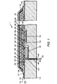
- Fig. 1 illustrates, in cross section, a hermetically sealed packaged electronic system, such as a hermetically sealed multichip integrated circuit package 1.
- Package 1 includes a substrate 110, which, in accordance with the invention, also serves as the base of the completed hermetic package.
- substrate 110 may, for example, have a thickness of about 0.635 to about 2.54 mm (25 to 100 mils) and may be comprised of alumina (Al 2 O 3 ) or aluminum nitride (AIN); alumina is preferred.
- a portion of a desired surface of substrate 110 i.e. a component supporting surface, includes a cavity 112 and a cavity 114.
- substrate 110 may be provided with a single cavity, or with more than two cavities.
- a plurality of electrical circuit components e.g. integrated circuit chips 124 and 126 having interconnection pads 128 thereon, are positioned within cavities 112 and 114, respectively.
- Cavities 112 and 114 may be formed by starting with a bare substrate having a uniform thickness and desired size. Conventional, laser or ultrasonic milling is used to produce the aforementioned cavities 112 and 114 in which various electronic components, such as very large scale integrated (VLSI) circuit chips, are to be positioned. Where a relatively thicker or relatively thinner electronic component will be placed, the corresponding cavity bottom is made respectively deeper or shallower.
- VLSI very large scale integrated
- the desired surface of substrate 110 is further provided with a plurality of module contact pads 116 which comprise electrically conductive materials, such as gold, aluminum, copper or tungsten. Tungsten is preferred. Pads 116 are preferably screen printed and then cofired with substrate 110 in a process described in greater detail hereinbelow with reference to FIG. 2A.
- FIG. 1 further shows a barrier support frame 118 disposed on the desired surface of substrate 110 and preferably shaped as a rectangular picture frame.
- Barrier support frame 118 is positioned on module contact pads 116 and serves as a boundary that divides contact pads 116 into outer portions 120, i.e. portions outside the perimeter of frame 118 and inner portions 122, i.e. portions within the perimeter of frame 118.
- Barrier support frame 118 is preferably comprised of glass but may alternatively comprise glass and ceramic. Size and shape of barrier support frame 118 is such that cavities 112, 114 and inner portions 122 of contact pads 116 are located within its perimeter.
- Barrier support frame 118 is provided with minimal thickness, preferably of about 50 to about 250 ⁇ m (about 2 to about 10 mils), to ensure proper application of polymer dielectric films 130 and 136, described hereinbelow. Barrier support frame 118 is preferably screen printed and then cofired with substrate 110.
- Outer portions 120 of module contact pad 116 are preferably provided with a corrosion resistant coating 117 of material such as gold.
- Individual leads 115 of a conventional lead frame (not shown) are attached to outer portions 120 of barrier support frame 118. It will be appreciated that, prior to actual mounting of packaged electronic system 1 on a printed circuit board, the conventional lead frame is severed from individual leads 115.
- thermoplastic adhesive layer 123 and 125 are preferably comprised of Ultem® polyetherimide, available from General Electric Company, Pittsfield, Massachusetts.
- a multi-layer HDI overcoat structure 133 is then built up to electrically interconnect the electronic components, such as chips 124 and 126 into an actual functioning system.
- a polymer dielectric film 130 preferably comprised of Kapton® polyimide produced by E.I. duPont de Nemours and Company, Wilmington, Delaware, having a thickness of about 12.5 to about 75 ⁇ m (about 0.5 to about 3 mil), is pretreated to promote adhesion.
- Polymer dielectric film 130 may be comprised of thermoplastic or thermosetting material.
- polymer dielectric film 130 is coated with Ultem polyetherimide resin or some other suitable thermoplastic resin layer (not shown) and then bonded to the top surfaces of chips 124 and 126 and to the desired surface of substrate 110 enclosed within barrier support frame 118.
- Ultem polyetherimide resin serves as a thermoplastic adhesive to hold film 130 in place.
- the aforementioned bonding is conducted under vacuum conditions to prevent air entrapment between film 130 and substrate 110, thereby improving adhesion between the two.
- polymer dielectric film 130 and the adhesive coating (not shown) underneath film 130 are perforated, preferably by a laser beam, to form via openings 132 aligned with at least some of interconnection pads 128 on chips 124 and 126 and inner portions 122 of module contact pads 116.
- Exemplary laser drilling techniques are disclosed by Eichelberger et al. in commonly assigned United States Patent Nos. 4,714,516 issued December 22, 1987 and 4,894,115 issued January 16, 1990; and by Loughran et al. in a commonly assigned United States Patent No. 4,764,485 issued August 16, 1988.
- Buildup of HDI overcoat structure 133 continues by depositing a pattern of metallized interconnection conductors 134 on polymer dielectric film 130 for providing electrical connection between at least some of interconnection contact pads 128 and inner portions 122 of module contact pads 116 through via openings 132.
- Interconnection conductors 134 may be patterned to form individual conductors while they are being applied over film 130, or they may be applied as a continuous layer and then patterned using conventional photoresist and etching techniques. However, the photoresist is preferably exposed to a laser beam, which is scanned relative to substrate 110 to provide an accurately aligned pattern of conductors 134.
- Metallized interconnection conductors 134 further comprise a layer of titanium (not shown) in direct contact with polymer dielectric film 130 and a layer of copper (not shown) deposited on top of the titanium layer.
- Exemplary techniques for forming interconnection conductors are disclosed by Wojnarowski et al. in commonly assigned United States Patent Nos. 4,780,177 issued October 25, 1988 and 4,842,677 issued June 27, 1989; and by Eichelberger et al. in a commonly assigned United States Patent No. 4,835,704 issued May 30, 1989. Any misposition of the individual electronic components, such as chips 124 and 126, and their interconnection pads 128, is compensated through use of an adaptive laser lithography system disclosed in the aforementioned United States Patent No. 4,835,704.
- An additional polymer dielectric film 136 with via openings 138 therein and a pattern of interconnection conductors 140 thereon is supplied as required on top of film 130 and conductors 134 to provide the remainder of the desired electrical connections among pads 128.
- Those skilled in the art will recognize that still further polymer dielectric films with the necessary patterns of interconnection conductors thereon (not shown) may be provided, if desired, on top of film 136 and conductors 140.
- Polymer dielectric films 130 and 136 cover the area enclosed by support barrier frame 118 and inner side of frame 118 closer to inner portions 122.
- a polymer barrier layer 142 preferably of Kapton polyimide film and having a thickness of about 12.5 to about 250 ⁇ m (about 0.5 to about 10 mil), is laminated on polymer dielectric film 136.
- the aforementioned adhesion techniques are preferably employed to laminate layer 142 to film 136.
- Polymer barrier layer 142 covers the entire area enclosed within barrier support frame 118, including film 136, and partially covers barrier support frame 118. Portions of polymer barrier layer 142 that extend beyond barrier support frame 118 are removed, preferably through ablation by an excimer laser.
- the edges of polymer dielectric films 130, 136 and polymer barrier layer 142 are provided with a smooth taper, preferably by means of an excimer laser.
- Packaged electronic system 1 further comprises a metal barrier layer 144 disposed on top of polymer barrier layer 142.
- Metal barrier layer 144 together with polymer barrier layer 142 provide the hermetic seal for packaged electronic system 1.
- Metal barrier layer 144 is preferably provided with an overall thickness of about 12.5 to about 50 ⁇ m (about 0.5 mil to about 2 mil) and is preferably comprised of a series of metal layers as described hereinbelow. Generally metal barrier layer 144 entirely seals the area enclosed within barrier support frame 118 and partially covers frame 118. Thus, no portion of polymer barrier layer 142, including its edges, is exposed to atmosphere.
- Metal barrier layer 144 preferably comprises a layer of chromium 145 having a thickness of about 750 Angstroms ( ⁇ ) to about 1500 ⁇ , preferably 1000 ⁇ , directly deposited on top of adhesion-promoted polymer barrier layer 142.
- Conventional deposition techniques such as sputtering, chemical vapor deposition, or electroless metal deposition are used to deposit the layer of chromium; sputtering techniques are preferred.
- Metal barrier layer 144 further comprises a layer of copper 149 having a thickness of about 0.75 to about 2 micrometer, preferably about 1 micrometer.
- Conventional deposition techniques, such as sputtering, chemical vapor deposition, or electrolytic metal deposition are used to deposit the layer of copper; electrolytic metal deposition is preferred.
- packaged electronic system 1 is provided with a protective layer 147 on metal barrier layer 144 to bridge voids 146 in layer 144.
- Protective layer 147 is generally comprised of an inorganic corrosion resistant material, preferably a solder material. Solder materials suitable for protective layer 147 are alloys of gold/tin, silver/tin and tin/rubidium; gold/tin alloy is preferred.
- the solder material is deposited on metal barrier layer 144 by conventional means, such as chemical vapor deposition, electroplating and the like, electroplating being preferred.
- the thickness of protective layer 147 is dependent on the size (i.e. area) of individual voids 146 and should be roughly equal to the void size. Generally, the thickness of protective layer 147 is less than about 25 ⁇ m (1 mil).
- protective layer 147 In order to further improve the bridging action of protective layer 147, it may be locally heated conventionally as by infrared heating, hot wire heating, directed hot gas reflow, or laser reflow such as an excimer laser, to reflow layer 147, with excimer laser heating being preferred.
- packaged electronic system 1 may be provided with a predetermined number of pin connectors.
- substrate 110 is provided with a hole 148.
- a conventional metal connector pin 150 is then embedded within a sleeve 152 of polymer dielectric material, such as Ultem polyetherimide, positioned in hole 148.
- a metal barrier coating 154 is provided on the exposed side of connector pin 150 to furnish a hermetic seal to the pin connectors generally used in packaged electronic systems.
- Metal barrier coating 154 is made of same materials as material barrier 144 and the same aforementioned methods are used for depositing metal barrier coating 154.
- FIGS. 2A and 2B show the aspect of the present invention wherein a portion of module contact pads 216 are buried within a substrate 210. Only outer portions 218 and inner portions 220 of module contact pads 216 are exposed.
- FIG 2B shows the final stage in a substrate fabrication process whereby substrate 210, module contact pad outer portions 218 and inner portions 220, and a buried first portion 217 and buried second portions 219 of module contact pads 216 form a cofired body, which also includes a barrier support frame 222.
- a conventional multilayer ceramic fabrication process is employed, wherein the finished substrate 210 (FIG. 2A) starts off as a distinct laminated structure of green ceramic tapes.
- Green ceramic tape generally includes plasticizers and binders.
- a monolithic structure is produced.
- Substrate 210 of FIG. 2B is comprised of the same material as substrate 110 in the aforementioned packaged electronic system of FIG. 1.
- first portion 217 of module contact pads 216 is preferably screen printed on the desired surface of first green substrate layer 210A.
- a second green substrate layer 210B, with necessary holes punched for vias and registration, is subjected to similar process steps.
- Second portions 219, outer portions 218, and inner portions 220 of module contact pads 216 as well as barrier support frame 222 are screen printed on second green substrate layer 210B.
- the aforementioned screen printing steps are preferably carried out under vacuum conditions.
- First green substrate layer 210A and second green substrate layer 210B are joined together to form a laminated substrate structure, which is then cofired in a sintering oven that employs a controlled atmosphere and temperature to produce monolithic substrate 210 (FIG. 2B) over a period of time.
- An initial stage, at a relatively lower temperature, is a binder burnout stage, which results in a relatively porous ceramic structure.
- the temperature is then increased to ultimately create a dense ceramic structure, thereby producing a hermetic cofired substrate. Since portions of module contact pads 216 are buried within substrate 210, support barrier frame 222 is electrically isolated from pads 216.
- support barrier frame 222 may be made of glass, glass/ceramic or metal, such as Kovar and molybdenum.
- Resulting substrate 210 is then provided with desired cavities, such as a cavity 214.
- FIG. 2B The other components of the embodiment of FIG. 2B but not shown in FIG. 2B are the same as those disclosed with respect to FIG. 1 and are fabricated by the same method as that disclosed hereinabove.
- the hermetically sealed packaged electronic system of the invention includes a lightweight, pliable and resilient hermetic seal, which can be subjected to conventional gross and fine leak tests without damage. Both the configuration and the methods described herein are economical and are readily achievable through simplified fabrication steps. It will further be recognized that the processing methods described herein provide significant advantages with respect to the physical and electrical characteristics of the resulting circuit packages.
Landscapes
- Structures Or Materials For Encapsulating Or Coating Semiconductor Devices Or Solid State Devices (AREA)
- Non-Metallic Protective Coatings For Printed Circuits (AREA)
- Production Of Multi-Layered Print Wiring Board (AREA)
- Casings For Electric Apparatus (AREA)
- Wire Bonding (AREA)
Claims (20)
- Système électronique à boítier hermétiquement scellé, comprenant :un substrat (110, 210) ;une pluralité de plages (116, 216) de contact de modules disposées sur une surface voulue dudit substrat ;une structure de support formant barrière (118, 222) disposée sur ladite surface voulue, ladite structure présentant un périmètre divisant chaque élément de ladite pluralité desdites plages de contact de modules en une portion intérieure (122, 220) et en une portion extérieure (120, 218) ;une pluralité de composants électroniques (124, 126) présentant des plages d'interconnexion (128) sur le dessus, tous lesdits composants étant positionnés à l'intérieur du périmètre de ladite structure de support formant barrière ;un film polymère diélectrique (130) recouvrant et pontant lesdits composants électroniques, ledit film polymère diélectrique présentant une pluralité d'ouvertures traversantes (132), chacune desdites ouvertures traversantes étant alignée avec au moins quelques-unes des plages d'interconnexion et desdites portions intérieures desdites plages de contact de modules ;un motif de conducteurs d'interconnexion (134) disposé sur ledit film polymère diélectrique et s'étendant à travers des ouvertures traversantes associées pour obtenir une connexion électrique entre au moins quelques-unes desdites plages d'interconnexion et lesdites portions intérieures desdites plages de contact de modules ;une couche barrière polymère (142) disposée sur ledit film polymère diélectrique de manière à couvrir entièrement une zone enfermée dans ladite structure de support formant barrière et à couvrir aussi partiellement ladite structure de support formant barrière sur toute sa périphérie ;une couche barrière métallique (144) disposée sur ladite couche barrière polymère et adhérant à ladite structure de support formant barrière sur toute sa périphérie de manière à couvrir entièrement une zone scellée enfermée dans ladite couche barrière polymère et ladite structure de support formant barrière ; etune couche protectrice (147) disposée sur ladite couche barrière polymère et comblant tous les vides qui peuvent être présents dans ladite couche barrière métallique de manière à sceller hermétiquement le volume délimité par ledit substrat, ladite structure de support formant barrière, ladite couche barrière métallique et ladite couche protectrice, caractérisé par le fait que lesdites plages (216) de contact de modules présentent une portion (217) enterrée dans ledit substrat.
- Système électronique à boítier hermétiquement scellé selon la revendication 1, dans lequel ledit substrat comprend de l'alumine ou du nitrure d'aluminium.
- Système électronique à boítier hermétiquement scellé selon la revendication 1, dans lequel ladite structure de support formant barrière comprend du verre ou un composite de verre et de céramique.
- Système électronique à boítier hermétiquement scellé selon la revendication 1, dans lequel ledit film polymère diélectrique comprend un matériau thermoplastique ou thermodurcissable.
- Système électronique à boítier hermétiquement scellé selon la revendication 1, dans lequel ledit motif d'interconnexion comprend en outre une couche de titane en contact avec ledit film polymère diélectrique et une couche de cuivre sur ladite couche de titane.
- Système électronique à boítier hermétiquement scellé selon la revendication 1, dans lequel ladite couche barrière métallique comprend en outre une couche (145) de chrome en contact avec ladite couche barrière polymère et une couche (149) de cuivre sur ladite couche de chrome.
- Système électronique à boítier hermétiquement scellé selon la revendication 1, dans lequel ladite couche protectrice comprend un alliage d'or et d'étain, ou d'argent et d'étain, ou de rubidium et d'étain.
- Système électronique à boítier hermétiquement scellé selon la revendication 1, dans lequel des bords phériphériques adjacents dudit film polymère diélectrique et de ladite couche barrière polymère sont biseautées uniment.
- Système électronique à boítier hermétiquement scellé selon la revendication 1, dans lequel chacun desdits composants électroniques comprend une puce de circuit intégré respective.
- Procédé de scellage hermétique d'un boítier (1) de circuit intégré à multiples puces, comprenant les étapes qui consistent à :déposer une première portion (217) d'une pluralité de plages (116, 216) de contact de modules sur une première couche de substrat en céramique crue (210A) et une seconde portion (219) de ladite pluralité desdites plages de contact de modules sur une seconde couche de substrat en céramique crue (210B) ;réunir lesdites première et seconde couches de substrat en céramique crue pour qu'un segment de ladite pluralité desdites plages de contact de modules soit enterré entre ladite première couche de substrat en céramique crue et ladite seconde couche de substrat en céramique crue ;déposer une structure de support formant barrière (118, 222) sur une surface voulue de ladite seconde couche de substrat en céramique crue pour que lesdites plages de contact de modules de ladite pluralité soient divisées en portions extérieures (120, 218) et en portions intérieures (122, 220) ;faire cuire en même temps lesdites première et seconde couches de substrat en céramique crue pour former un substrat (110, 210) à partir de ces dernières ;positionner sur ladite surface voulue, une pluralité de puces de circuit intégré (124, 126) présentant sur le dessus des plages d'interconnexion (128), lesdites puces de circuit intégré étant situées à l'intérieur du périmètre de ladite structure de support formant barrière ;appliquer un film polymère diélectrique (130) pour couvrir ladite pluralité de puces de circuit intégré et ladite surface voulue à l'intérieur du périmètre de ladite structure de support formant barrière, et se lier à elles ;perforer ledit film polymère diélectrique pour y former des ouvertures traversantes (132), lesdites ouvertures étant alignées avec au moins certaines desdites plages d'interconnexion et portions intérieures desdites plages de contact de modules ;déposer un motif de conducteurs d'interconnexion (134) sur ledit film polymère diélectrique pour obtenir une connexion électrique entre au moins certaines desdites plages d'interconnexion et desdites portions intérieures desdites plages de contact de modules ;stratifier une couche barrière polymère (142) sur ledit film polymère diélectrique pour couvrir entièrement la zone enfermée dans la structure de support formant barrière et pour couvrir partiellement ladite structure de support formant barrière ;déposer une couche métallique barrière (144) sur ladite couche barrière polymère pour couvrir entièrement la zone enfermée dans ladite couche barrière polymère et pour sensiblement recouvrir ledit pourtour de ladite structure de support formant barrière ; et àdéposer une couche protectrice (147) sur ladite couche barrière métallique pour combler tous les vides qui peuvent être présents dans ladite couche barrière métallique.
- Procédé selon la revendication 10, dans lequel ladite structure de support formant barrière comprend l'un des éléments du groupe constitué par le verre et un métal.
- Procédé selon la revendication 10, dans lequel l'étape consistant à déposer ladite pluralité desdites plages de contact de modules comprend en outre le dépôt d'un revêtement conducteur résistant à la corrosion (117) sur lesdites portions extérieures desdites plages de contact de modules.
- Procédé selon la revendication 10, dans lequel l'étape consistant à déposer ladite pluralité desdites plages de contact de modules comprend la sérigraphie desdites plages de contact de modules sur ladite surface voulue.
- Procédé selon la revendication 10, dans lequel l'étape consistant à déposer ladite structure de support formant barrière comprend la sérigraphie de ladite structure de support formant barrière sur ladite surface voulue.
- Procédé selon la revendication 10, dans lequel ladite structure de support formant barrière est constituée de verre.
- Procédé selon la revendication 10, dans lequel l'étape consistant à stratifier une couche barrière polymère sur ledit film polymère diélectrique englobe l'étape consistant à éliminer des portions de ladite couche polymère barrière qui s'étendent au-delà du périmètre de ladite structure de support formant barrière.
- Procédé selon la revendication 16, comprenant en outre l'étape consistant à biseauter uniment des bords dudit film polymère diélectrique et de ladite couche barrière polymère.
- Procédé selon la revendication 16, dans lequel l'étape consistant à éliminer des portions de ladite couche polymère barrière comprend l'étape consistant à enlever lesdites portions de ladite couche polymère barrière avec un laser à excimères.
- Procédé selon la revendication 10, dans lequel l'étape consistant à déposer une couche barrière métallique comprend l'une des opérations consistant à déposer par pulvérisation cathodique ou à effectuer un dépôt chimique en phase vapeur de ladite couche barrière métallique sur ladite couche polymère barrière.
- Procédé selon la revendication 10, comprenant l'étape supplémentaire consistant à chauffer ladite couche protectrice de façon à améliorer le comblement desdits vides dans ladite couche barrière métallique.
Applications Claiming Priority (2)
| Application Number | Priority Date | Filing Date | Title |
|---|---|---|---|
| US947190 | 1992-09-18 | ||
| US07/947,190 US5336928A (en) | 1992-09-18 | 1992-09-18 | Hermetically sealed packaged electronic system |
Publications (3)
| Publication Number | Publication Date |
|---|---|
| EP0588603A2 EP0588603A2 (fr) | 1994-03-23 |
| EP0588603A3 EP0588603A3 (fr) | 1994-10-26 |
| EP0588603B1 true EP0588603B1 (fr) | 1999-03-24 |
Family
ID=25485692
Family Applications (1)
| Application Number | Title | Priority Date | Filing Date |
|---|---|---|---|
| EP93307249A Expired - Lifetime EP0588603B1 (fr) | 1992-09-18 | 1993-09-14 | Boítier pour système électronique scellé hermétiquement et procédé pour sa fabrication |
Country Status (4)
| Country | Link |
|---|---|
| US (1) | US5336928A (fr) |
| EP (1) | EP0588603B1 (fr) |
| JP (1) | JPH06224266A (fr) |
| DE (1) | DE69324088T2 (fr) |
Families Citing this family (60)
| Publication number | Priority date | Publication date | Assignee | Title |
|---|---|---|---|---|
| JPH06209058A (ja) * | 1993-01-12 | 1994-07-26 | Mitsubishi Electric Corp | 半導体装置及びその製造方法,並びにその実装方法 |
| US5593927A (en) * | 1993-10-14 | 1997-01-14 | Micron Technology, Inc. | Method for packaging semiconductor dice |
| US5637922A (en) * | 1994-02-07 | 1997-06-10 | General Electric Company | Wireless radio frequency power semiconductor devices using high density interconnect |
| US5552232A (en) * | 1994-12-21 | 1996-09-03 | International Business Machines Corporation | Aluminum nitride body having graded metallurgy |
| US5744752A (en) * | 1995-06-05 | 1998-04-28 | International Business Machines Corporation | Hermetic thin film metallized sealband for SCM and MCM-D modules |
| US5851845A (en) * | 1995-12-18 | 1998-12-22 | Micron Technology, Inc. | Process for packaging a semiconductor die using dicing and testing |
| US5682065A (en) * | 1996-03-12 | 1997-10-28 | Micron Technology, Inc. | Hermetic chip and method of manufacture |
| DE19614458C2 (de) * | 1996-04-12 | 1998-10-29 | Grundfos As | Druck- oder Differenzdrucksensor und Verfahren zu seiner Herstellung |
| DE19614459A1 (de) * | 1996-04-12 | 1997-10-16 | Grundfos As | Elektronisches Bauelement |
| US6667560B2 (en) | 1996-05-29 | 2003-12-23 | Texas Instruments Incorporated | Board on chip ball grid array |
| JP3695893B2 (ja) * | 1996-12-03 | 2005-09-14 | 沖電気工業株式会社 | 半導体装置とその製造方法および実装方法 |
| US6036084A (en) * | 1997-02-06 | 2000-03-14 | Tdk Corporation | Screen printing method and apparatus therefor, and electronic component soldering method using screen printing and apparatus therefor |
| US6150719A (en) * | 1997-07-28 | 2000-11-21 | General Electric Company | Amorphous hydrogenated carbon hermetic structure and fabrication method |
| US6127038A (en) * | 1997-12-11 | 2000-10-03 | American Meter Company | Printed circuit board coating and method |
| NL1008353C2 (nl) * | 1998-02-19 | 1999-08-20 | Nedap Nv | Spoel- en verbindingsconstructie voor een contactloos label. |
| US6008070A (en) * | 1998-05-21 | 1999-12-28 | Micron Technology, Inc. | Wafer level fabrication and assembly of chip scale packages |
| US6084306A (en) * | 1998-05-29 | 2000-07-04 | Texas Instruments Incorporated | Bridging method of interconnects for integrated circuit packages |
| KR100424188B1 (ko) * | 1998-09-21 | 2004-05-17 | 주식회사 하이닉스반도체 | 칩 사이즈 스택 패키지 |
| US6121672A (en) * | 1998-11-03 | 2000-09-19 | Utmc Microelectronic Systems Inc. | Raised pedestal radiation shield for sensitive electronics |
| JP3214470B2 (ja) * | 1998-11-16 | 2001-10-02 | 日本電気株式会社 | マルチチップモジュール及びその製造方法 |
| US6544880B1 (en) * | 1999-06-14 | 2003-04-08 | Micron Technology, Inc. | Method of improving copper interconnects of semiconductor devices for bonding |
| DE69933380T2 (de) * | 1999-12-15 | 2007-08-02 | Asulab S.A. | Verfahren zum hermetischen Einkapseln von Mikrosystemen vor Ort |
| US6524881B1 (en) | 2000-08-25 | 2003-02-25 | Micron Technology, Inc. | Method and apparatus for marking a bare semiconductor die |
| US6528875B1 (en) * | 2001-04-20 | 2003-03-04 | Amkor Technology, Inc. | Vacuum sealed package for semiconductor chip |
| WO2002100769A2 (fr) * | 2001-06-08 | 2002-12-19 | The Regents Of The University Of Michigan | Technique d'encapsulation de circuit utilisant le depot electrolytique |
| KR100488412B1 (ko) * | 2001-06-13 | 2005-05-11 | 가부시키가이샤 덴소 | 내장된 전기소자를 갖는 인쇄 배선 기판 및 그 제조 방법 |
| US6720561B2 (en) | 2001-12-06 | 2004-04-13 | General Electric Company | Direct CsI scintillator coating for improved digital X-ray detector assembly longevity |
| US7053381B2 (en) | 2001-12-06 | 2006-05-30 | General Electric Company | Dual para-xylylene layers for an X-ray detector |
| TW584950B (en) | 2001-12-31 | 2004-04-21 | Megic Corp | Chip packaging structure and process thereof |
| TW503496B (en) | 2001-12-31 | 2002-09-21 | Megic Corp | Chip packaging structure and manufacturing process of the same |
| TW517361B (en) | 2001-12-31 | 2003-01-11 | Megic Corp | Chip package structure and its manufacture process |
| US6673698B1 (en) | 2002-01-19 | 2004-01-06 | Megic Corporation | Thin film semiconductor package utilizing a glass substrate with composite polymer/metal interconnect layers |
| TW544882B (en) | 2001-12-31 | 2003-08-01 | Megic Corp | Chip package structure and process thereof |
| TW200302685A (en) * | 2002-01-23 | 2003-08-01 | Matsushita Electric Industrial Co Ltd | Circuit component built-in module and method of manufacturing the same |
| US7169685B2 (en) | 2002-02-25 | 2007-01-30 | Micron Technology, Inc. | Wafer back side coating to balance stress from passivation layer on front of wafer and be used as die attach adhesive |
| US6641254B1 (en) | 2002-04-12 | 2003-11-04 | Hewlett-Packard Development Company, L.P. | Electronic devices having an inorganic film |
| US6964881B2 (en) * | 2002-08-27 | 2005-11-15 | Micron Technology, Inc. | Multi-chip wafer level system packages and methods of forming same |
| US6768196B2 (en) * | 2002-09-04 | 2004-07-27 | Analog Devices, Inc. | Packaged microchip with isolation |
| US6946742B2 (en) * | 2002-12-19 | 2005-09-20 | Analog Devices, Inc. | Packaged microchip with isolator having selected modulus of elasticity |
| US20040041254A1 (en) * | 2002-09-04 | 2004-03-04 | Lewis Long | Packaged microchip |
| US7166911B2 (en) | 2002-09-04 | 2007-01-23 | Analog Devices, Inc. | Packaged microchip with premolded-type package |
| US6861343B2 (en) * | 2002-10-09 | 2005-03-01 | Chok J. Chia | Buffer metal layer |
| US20050056870A1 (en) * | 2002-12-19 | 2005-03-17 | Karpman Maurice S. | Stress sensitive microchip with premolded-type package |
| US20050173812A1 (en) * | 2004-02-06 | 2005-08-11 | Howard Morgenstern | Microsystem enclosure and method of hermetic sealing |
| KR20070006682A (ko) * | 2004-03-30 | 2007-01-11 | 허니웰 인터내셔널 인코포레이티드 | 히트 스프레더 구조물, 집적 회로, 및 그들의 제조방법 |
| US7045827B2 (en) * | 2004-06-24 | 2006-05-16 | Gallup Kendra J | Lids for wafer-scale optoelectronic packages |
| DE102004057494A1 (de) * | 2004-11-29 | 2006-06-08 | Siemens Ag | Metallisierte Folie zur flächigen Kontaktierung |
| WO2006098813A1 (fr) | 2005-02-01 | 2006-09-21 | Second Sight Medical Products, Inc. | Dispositif implantable revetu microminiaturise |
| CN100514591C (zh) * | 2005-03-02 | 2009-07-15 | 皇家飞利浦电子股份有限公司 | 半导体封装的制造方法及所制成的封装 |
| WO2008003051A2 (fr) * | 2006-06-29 | 2008-01-03 | Analog Devices, Inc. | Atténuation des contraintes dans Des microcircuits en boîtier |
| SE532372C2 (sv) * | 2007-03-21 | 2009-12-29 | Lars Haakan Wernersson | Fjädrande infästande arrangemang |
| US7694610B2 (en) * | 2007-06-27 | 2010-04-13 | Siemens Medical Solutions Usa, Inc. | Photo-multiplier tube removal tool |
| US8161811B2 (en) | 2009-12-18 | 2012-04-24 | Honeywell International Inc. | Flow sensors having nanoscale coating for corrosion resistance |
| US9676614B2 (en) | 2013-02-01 | 2017-06-13 | Analog Devices, Inc. | MEMS device with stress relief structures |
| US10167189B2 (en) | 2014-09-30 | 2019-01-01 | Analog Devices, Inc. | Stress isolation platform for MEMS devices |
| US10131538B2 (en) | 2015-09-14 | 2018-11-20 | Analog Devices, Inc. | Mechanically isolated MEMS device |
| US10399256B1 (en) * | 2018-04-17 | 2019-09-03 | Goodrich Corporation | Sealed circuit card assembly |
| US11417611B2 (en) | 2020-02-25 | 2022-08-16 | Analog Devices International Unlimited Company | Devices and methods for reducing stress on circuit components |
| US11981560B2 (en) | 2020-06-09 | 2024-05-14 | Analog Devices, Inc. | Stress-isolated MEMS device comprising substrate having cavity and method of manufacture |
| US20250118715A1 (en) | 2022-01-25 | 2025-04-10 | Analog Devices, Inc. | Microelectromechanical systems (mems) and related packages |
Family Cites Families (20)
| Publication number | Priority date | Publication date | Assignee | Title |
|---|---|---|---|---|
| US4477828A (en) * | 1982-10-12 | 1984-10-16 | Scherer Jeremy D | Microcircuit package and sealing method |
| JPS6119154A (ja) * | 1984-07-05 | 1986-01-28 | Nec Corp | 樹脂封止型半導体装置 |
| JPS62197379A (ja) * | 1986-02-20 | 1987-09-01 | 株式会社東芝 | 窒化アルミニウム基板 |
| US4884122A (en) * | 1988-08-05 | 1989-11-28 | General Electric Company | Method and configuration for testing electronic circuits and integrated circuit chips using a removable overlay layer |
| US4714516A (en) * | 1986-09-26 | 1987-12-22 | General Electric Company | Method to produce via holes in polymer dielectrics for multiple electronic circuit chip packaging |
| US4937203A (en) * | 1986-09-26 | 1990-06-26 | General Electric Company | Method and configuration for testing electronic circuits and integrated circuit chips using a removable overlay layer |
| US4783695A (en) * | 1986-09-26 | 1988-11-08 | General Electric Company | Multichip integrated circuit packaging configuration and method |
| DE3784213T2 (de) * | 1986-10-29 | 1993-06-03 | Toshiba Kawasaki Kk | Elektronischer apparat mit einem keramischen substrat. |
| US4835704A (en) * | 1986-12-29 | 1989-05-30 | General Electric Company | Adaptive lithography system to provide high density interconnect |
| US4764485A (en) * | 1987-01-05 | 1988-08-16 | General Electric Company | Method for producing via holes in polymer dielectrics |
| US4780177A (en) * | 1988-02-05 | 1988-10-25 | General Electric Company | Excimer laser patterning of a novel resist |
| US4842677A (en) * | 1988-02-05 | 1989-06-27 | General Electric Company | Excimer laser patterning of a novel resist using masked and maskless process steps |
| US4840302A (en) * | 1988-04-15 | 1989-06-20 | International Business Machines Corporation | Chromium-titanium alloy |
| US4878991A (en) * | 1988-12-12 | 1989-11-07 | General Electric Company | Simplified method for repair of high density interconnect circuits |
| US4894115A (en) * | 1989-02-14 | 1990-01-16 | General Electric Company | Laser beam scanning method for forming via holes in polymer materials |
| US4999700A (en) * | 1989-04-20 | 1991-03-12 | Honeywell Inc. | Package to board variable pitch tab |
| JPH03211757A (ja) * | 1989-12-21 | 1991-09-17 | General Electric Co <Ge> | 気密封じの物体 |
| US5081563A (en) * | 1990-04-27 | 1992-01-14 | International Business Machines Corporation | Multi-layer package incorporating a recessed cavity for a semiconductor chip |
| US5073814A (en) * | 1990-07-02 | 1991-12-17 | General Electric Company | Multi-sublayer dielectric layers |
| EP0547807A3 (en) * | 1991-12-16 | 1993-09-22 | General Electric Company | Packaged electronic system |
-
1992
- 1992-09-18 US US07/947,190 patent/US5336928A/en not_active Expired - Fee Related
-
1993
- 1993-09-14 EP EP93307249A patent/EP0588603B1/fr not_active Expired - Lifetime
- 1993-09-14 DE DE69324088T patent/DE69324088T2/de not_active Expired - Fee Related
- 1993-09-16 JP JP5229379A patent/JPH06224266A/ja not_active Withdrawn
Also Published As
| Publication number | Publication date |
|---|---|
| EP0588603A3 (fr) | 1994-10-26 |
| DE69324088T2 (de) | 1999-10-14 |
| EP0588603A2 (fr) | 1994-03-23 |
| US5336928A (en) | 1994-08-09 |
| JPH06224266A (ja) | 1994-08-12 |
| DE69324088D1 (de) | 1999-04-29 |
Similar Documents
| Publication | Publication Date | Title |
|---|---|---|
| EP0588603B1 (fr) | Boítier pour système électronique scellé hermétiquement et procédé pour sa fabrication | |
| US5359496A (en) | Hermetic high density interconnected electronic system | |
| US5315486A (en) | Hermetically packaged HDI electronic system | |
| US5527741A (en) | Fabrication and structures of circuit modules with flexible interconnect layers | |
| US5224265A (en) | Fabrication of discrete thin film wiring structures | |
| US5157589A (en) | Mutliple lamination high density interconnect process and structure employing thermoplastic adhesives having sequentially decreasing TG 's | |
| US5232548A (en) | Discrete fabrication of multi-layer thin film, wiring structures | |
| CN100556233C (zh) | 制造电子模块的方法以及电子模块 | |
| EP0130417B1 (fr) | Méthode pour fabriquer une structure électrique de connexion intermédiaire pour un module intégré | |
| US5386627A (en) | Method of fabricating a multi-layer integrated circuit chip interposer | |
| EP0450950B1 (fr) | Structure d'interconnexion flexible à haute densité | |
| US5744758A (en) | Multilayer circuit board and process of production thereof | |
| US5199163A (en) | Metal transfer layers for parallel processing | |
| US5412539A (en) | Multichip module with a mandrel-produced interconnecting decal | |
| KR100257926B1 (ko) | 회로기판형성용다층필름 및 이를 사용한 다층회로기판 및 반도체장치용패키지 | |
| JPH04251969A (ja) | 電子装置 | |
| US20080128911A1 (en) | Semiconductor package and method for manufacturing the same | |
| WO1986003337A1 (fr) | Procede de fabrication de modules d'interconnexion dimensionnellement stables et produit obtenu par ce procede | |
| WO1997022146A1 (fr) | Boitier de semi-conducteur comportant un circuit a couches multiples et composant a semi-conducteur | |
| WO2000025558A1 (fr) | Carte a circuits et procede de fabrication de cette carte | |
| CA2024784C (fr) | Substrat multicouche empilable pour le montage des circuits integres | |
| JPH0799265A (ja) | 多層配線基板および多層配線基板の製造方法 | |
| US20050121225A1 (en) | Multi-layer circuit board and method for fabricating the same | |
| JP2549393B2 (ja) | 回路基板の製造方法 | |
| US5094969A (en) | Method for making a stackable multilayer substrate for mounting integrated circuits |
Legal Events
| Date | Code | Title | Description |
|---|---|---|---|
| PUAI | Public reference made under article 153(3) epc to a published international application that has entered the european phase |
Free format text: ORIGINAL CODE: 0009012 |
|
| AK | Designated contracting states |
Kind code of ref document: A2 Designated state(s): DE FR GB IT NL |
|
| PUAL | Search report despatched |
Free format text: ORIGINAL CODE: 0009013 |
|
| AK | Designated contracting states |
Kind code of ref document: A3 Designated state(s): DE FR GB IT NL |
|
| 17P | Request for examination filed |
Effective date: 19950426 |
|
| 17Q | First examination report despatched |
Effective date: 19960802 |
|
| GRAG | Despatch of communication of intention to grant |
Free format text: ORIGINAL CODE: EPIDOS AGRA |
|
| GRAG | Despatch of communication of intention to grant |
Free format text: ORIGINAL CODE: EPIDOS AGRA |
|
| GRAH | Despatch of communication of intention to grant a patent |
Free format text: ORIGINAL CODE: EPIDOS IGRA |
|
| GRAH | Despatch of communication of intention to grant a patent |
Free format text: ORIGINAL CODE: EPIDOS IGRA |
|
| GRAA | (expected) grant |
Free format text: ORIGINAL CODE: 0009210 |
|
| AK | Designated contracting states |
Kind code of ref document: B1 Designated state(s): DE FR GB IT NL |
|
| RIN1 | Information on inventor provided before grant (corrected) |
Inventor name: WOJNAROWSKI, ROBERT JOHN Inventor name: NEUGEBAUER, CONSTANTINE ALOIS |
|
| ET | Fr: translation filed | ||
| REF | Corresponds to: |
Ref document number: 69324088 Country of ref document: DE Date of ref document: 19990429 |
|
| PG25 | Lapsed in a contracting state [announced via postgrant information from national office to epo] |
Ref country code: GB Free format text: LAPSE BECAUSE OF NON-PAYMENT OF DUE FEES Effective date: 19990914 |
|
| PLBE | No opposition filed within time limit |
Free format text: ORIGINAL CODE: 0009261 |
|
| STAA | Information on the status of an ep patent application or granted ep patent |
Free format text: STATUS: NO OPPOSITION FILED WITHIN TIME LIMIT |
|
| 26N | No opposition filed | ||
| PG25 | Lapsed in a contracting state [announced via postgrant information from national office to epo] |
Ref country code: NL Free format text: LAPSE BECAUSE OF NON-PAYMENT OF DUE FEES Effective date: 20000401 |
|
| GBPC | Gb: european patent ceased through non-payment of renewal fee |
Effective date: 19990914 |
|
| PG25 | Lapsed in a contracting state [announced via postgrant information from national office to epo] |
Ref country code: FR Free format text: LAPSE BECAUSE OF NON-PAYMENT OF DUE FEES Effective date: 20000531 |
|
| NLV4 | Nl: lapsed or anulled due to non-payment of the annual fee |
Effective date: 20000401 |
|
| PG25 | Lapsed in a contracting state [announced via postgrant information from national office to epo] |
Ref country code: DE Free format text: LAPSE BECAUSE OF NON-PAYMENT OF DUE FEES Effective date: 20000701 |
|
| REG | Reference to a national code |
Ref country code: FR Ref legal event code: ST |
|
| PG25 | Lapsed in a contracting state [announced via postgrant information from national office to epo] |
Ref country code: IT Free format text: LAPSE BECAUSE OF NON-PAYMENT OF DUE FEES Effective date: 20050914 |