EP0589622A1 - Verfahren zum Ausrichten von Vorrichtungen - Google Patents
Verfahren zum Ausrichten von Vorrichtungen Download PDFInfo
- Publication number
- EP0589622A1 EP0589622A1 EP93307300A EP93307300A EP0589622A1 EP 0589622 A1 EP0589622 A1 EP 0589622A1 EP 93307300 A EP93307300 A EP 93307300A EP 93307300 A EP93307300 A EP 93307300A EP 0589622 A1 EP0589622 A1 EP 0589622A1
- Authority
- EP
- European Patent Office
- Prior art keywords
- machine vision
- vision camera
- laser
- computer
- devices
- Prior art date
- Legal status (The legal status is an assumption and is not a legal conclusion. Google has not performed a legal analysis and makes no representation as to the accuracy of the status listed.)
- Ceased
Links
- 238000000034 method Methods 0.000 title claims description 23
- 239000013307 optical fiber Substances 0.000 claims abstract description 36
- 230000003287 optical effect Effects 0.000 claims description 9
- 238000003384 imaging method Methods 0.000 claims description 8
- 239000000835 fiber Substances 0.000 description 14
- 238000003491 array Methods 0.000 description 3
- 238000004519 manufacturing process Methods 0.000 description 3
- 230000000712 assembly Effects 0.000 description 2
- 238000000429 assembly Methods 0.000 description 2
- 239000000523 sample Substances 0.000 description 2
- 239000004065 semiconductor Substances 0.000 description 2
- 239000004593 Epoxy Substances 0.000 description 1
- 230000005540 biological transmission Effects 0.000 description 1
- 238000012937 correction Methods 0.000 description 1
- 230000008878 coupling Effects 0.000 description 1
- 238000010168 coupling process Methods 0.000 description 1
- 238000005859 coupling reaction Methods 0.000 description 1
- 230000001627 detrimental effect Effects 0.000 description 1
- 238000011161 development Methods 0.000 description 1
- 238000010894 electron beam technology Methods 0.000 description 1
- 238000012986 modification Methods 0.000 description 1
- 230000004048 modification Effects 0.000 description 1
- 238000004806 packaging method and process Methods 0.000 description 1
- 229910000679 solder Inorganic materials 0.000 description 1
- YLJREFDVOIBQDA-UHFFFAOYSA-N tacrine Chemical compound C1=CC=C2C(N)=C(CCCC3)C3=NC2=C1 YLJREFDVOIBQDA-UHFFFAOYSA-N 0.000 description 1
- 229960001685 tacrine Drugs 0.000 description 1
- 230000000007 visual effect Effects 0.000 description 1
Images


Classifications
-
- G—PHYSICS
- G02—OPTICS
- G02B—OPTICAL ELEMENTS, SYSTEMS OR APPARATUS
- G02B7/00—Mountings, adjusting means, or light-tight connections, for optical elements
- G02B7/003—Alignment of optical elements
- G02B7/005—Motorised alignment
-
- G—PHYSICS
- G02—OPTICS
- G02B—OPTICAL ELEMENTS, SYSTEMS OR APPARATUS
- G02B6/00—Light guides; Structural details of arrangements comprising light guides and other optical elements, e.g. couplings
- G02B6/24—Coupling light guides
- G02B6/42—Coupling light guides with opto-electronic elements
- G02B6/4201—Packages, e.g. shape, construction, internal or external details
- G02B6/4219—Mechanical fixtures for holding or positioning the elements relative to each other in the couplings; Alignment methods for the elements, e.g. measuring or observing methods especially used therefor
- G02B6/422—Active alignment, i.e. moving the elements in response to the detected degree of coupling or position of the elements
- G02B6/4221—Active alignment, i.e. moving the elements in response to the detected degree of coupling or position of the elements involving a visual detection of the position of the elements, e.g. by using a microscope or a camera
Definitions
- This invention relates to methods and apparatus for aligning devices and, more particularly, to methods for aligning optical or photonics devices with a high degree of precision.
- the optical fiber For automatic assembly of laser modules using active alignment, it is usually required that some apparatus be devised for causing one end of the optical fiber to scan a small area intercepting the laser output beam, while a photodetector at the output end of the fiber detects the location at which maximum light transmission occurs. When that position has been determined, the optical fiber is permanently bonded to the laser and enclosed within a package.
- first and second devices such as a laser and an optical fiber
- first and second devices are aligned by first positioning the laser on an x-y-z table (such a table is capable of responding to electrical signals to make precise movements in mutually orthogonal x , y and z directions).
- the laser beam is imaged onto a machine vision camera which develops signals representing the image of the laser beam and directs them to a computer.
- the computer analyzes the signal, calculates the center of the image, and determines from such calculation any deviations in the x and y directions of the position of the laser from its desired alignment position.
- the optical fiber is imaged on a machine vision camera.
- Signals from the camera representative of the image of the optical fiber end are directed to the computer which calculates the center of the image and determines any deviation from its desired position.
- the x-y-z table is moved such that the laser is in approximate alignment with the optical fiber end, and signals from the computer are used to make fine adjustments of the position of the x-y-z table to compensate for the deviations of the laser from its assigned position and deviations of the optical fiber end from its assigned position.
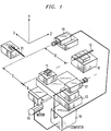
- FIG. 1 there is shown schematically an illustrative embodiment of the invention comprising apparatus for aligning and bonding together a semiconductor laser 11 and an optical fiber 12.
- the laser is mounted on an x-y-z table 13 which is capable of moving the laser in orthogonal x-y-z directions either in large increments or in incremental steps as small as 0.01 microns.
- the table is driven by a motor schematically shown at 15 which is controlled by signals from a computer 16.
- the x-y-z table may be of a type which is commercially available from the Anorad Corporation of Hauppauge New York, U.S.A.
- Also mounted on the x-y-z table is a machine vision camera 17.
- the optical fiber 12 is in approximate axial alignment with the laser 11 as is required for bonding them together, but it is located on a stationary support 18. Also located on a stationary support is a machine vision camera 19. Machine vision cameras is 17 and 19 are preferably conventional television cameras, but their function is to generate machine-readable video signals rather than video signals for visual display. Accordingly, any device, such as an array of photodetectors, capable of generating machine-readable signals representative of an image could be used as a machine vision camera.
- the outputs of machine vision cameras 17 and 19 are connected to the computer 16.
- the aligned photodetector and fiber are separated from camera 17 by a distance D and from camera 19 by a distance D. Also separated by a distance D from the laser 11 is an electronic probe 21 for biasing the laser 11.
- FIG. 1 shows the laser 11 being in alignment with the central axis of the optical fiber
- alignment can initially be made only approximately, and it is the purpose of this embodiment to adjust the alignment to be exact to within a fraction of a micron.
- the elements be aligned to maximize the portion of light emitted from the laser that is intercepted and transmitted by the core of the fiber which lies along the central axis of the fiber.
- the first step in accomplishing this function is to move the x-y-z table 13 in the x direction a distance D, to the position shown in FIG. 2.
- the probe 21 contacts the laser 11 which, when appropriately energized, emits light in the direction of machine vision camera 19.
- the laser 11 is in approximate alignment with machine vision camera 19, and consequently the emitted laser beam is easily within the field of view of the camera 19.
- the camera 19 contains lenses for imaging the laser light, and an electron beam for scanning the image to generate a video signal representative of the image.
- the video signal is directed to a computer 16 which is programmed to locate the geometrical center of the image.
- Machine vision systems including computers are well-known in the art, and one that is capable of producing the appropriate signals is a system available from Cognex, Inc., Needham, Massachusetts.
- the computer after determining the center of the laser beam, compares its location, such as location 22, with a location 23 that would represent perfect alignment.
- the difference of position of locations 22 and 23 represents the misalignment, or deviation from precise alignment, of the laser beam.
- a machine vision camera 17 generates signals representative of the image of the end of optical fiber 12 which are directed to the computer for determination of the geometric center at the end of fiber 12.
- camera 17 is in approximate alignment with optical fiber 12, and therefore the end of the optical fiber, in a section taken transverse to the fiber central axis, is within the field of view of the camera 17.
- the x-y-z table 13 is extremely accurate in its mechanical movements so it is capable of returning to the exact position shown in FIG. 1.
- This function can be stated as follows: If the initial misalignment of the laser is A x ,A y and the initial misalignment of the fiber is B x ,B y , the computer generates a corrective signal equal to (A x -B x ), (A y -B y ) to bring the laser into alignment with the fiber. Programming the computer to perform this simple function is within the skill of the worker in the art.
- the computer After alignment, the computer causes the x-y-z table to move in the z direction to bring the laser into sufficient proximity with the optical fiber 12 that they can be bonded.
- This is schematically shown in FIG. 4 where a mounting element 26 is shown as being bonded both to laser 11 and optical fiber 12.
- the bonding can be made by epoxy, solder, or other methods as are known in the art and can be done manually or automatically through the use of robotic apparatus known in the art.
- An advantage of the alignment scheme that has been described is that it can be operated automatically at a higher production rate than the active alignment method of aligning an optical fiber with a laser. This is important in the mass production of laser assemblies where many such identical assemblies may be required for a complex optical communications system. While a preferred method of aligning a laser with a fiber has been described, it is to be understood that other devices such as lenses, mirrors, photodetectors, etc., could be aligned and assembled by the same method and that significant deviations from the method shown could be made.
- the laser beam is imaged on the machine vision camera, but it is to be understood that this is the equivalent of imaging the laser device on the machine vision camera and that the method aligns the laser device, as well as the beam, with the optical fiber.
- aligning the laser while it emits light is preferable because it assures alignment of the center of emitted light with the center of the optical fiber. While it is advantageous to have the two cameras each located a distance D from the aligned fiber and laser as shown so that one movement of the x-y-z table will bring both cameras into alignment, such configuration is not essential.
- the invention can be used to align laser arrays or photodetector arrays with fiber bundles or lens arrays. Other embodiments and modifications may be made by those skilled in the art without departing from the spirit and scope of the invention.
Landscapes
- Physics & Mathematics (AREA)
- General Physics & Mathematics (AREA)
- Optics & Photonics (AREA)
- Optical Couplings Of Light Guides (AREA)
- Mounting And Adjusting Of Optical Elements (AREA)
Applications Claiming Priority (2)
| Application Number | Priority Date | Filing Date | Title |
|---|---|---|---|
| US07/948,543 US5383118A (en) | 1992-09-23 | 1992-09-23 | Device alignment methods |
| US948543 | 1992-09-23 |
Publications (1)
| Publication Number | Publication Date |
|---|---|
| EP0589622A1 true EP0589622A1 (de) | 1994-03-30 |
Family
ID=25487976
Family Applications (1)
| Application Number | Title | Priority Date | Filing Date |
|---|---|---|---|
| EP93307300A Ceased EP0589622A1 (de) | 1992-09-23 | 1993-09-16 | Verfahren zum Ausrichten von Vorrichtungen |
Country Status (3)
| Country | Link |
|---|---|
| US (1) | US5383118A (de) |
| EP (1) | EP0589622A1 (de) |
| JP (1) | JPH06194607A (de) |
Cited By (11)
| Publication number | Priority date | Publication date | Assignee | Title |
|---|---|---|---|---|
| EP0778481A1 (de) * | 1995-12-07 | 1997-06-11 | Deutsche Telekom AG | Verfahren zum Herstellen und präzisen Positionieren von optischen Mikrolinsen auf den Enden von Fasern und Lasern |
| EP0760489A3 (de) * | 1995-08-31 | 1998-01-14 | Fujitsu Limited | Zusammenbau eines optischen Moduls |
| EP1219996A3 (de) * | 2000-12-28 | 2002-08-28 | Japan Aviation Electronics Industry, Limited | Optisches Modul und Methode der Montage des optischen Modul |
| WO2002052324A3 (en) * | 2000-12-26 | 2003-01-09 | Emcore Corp | Process for coupling optical elements to optoelectronic devices |
| WO2003002930A3 (en) * | 2001-06-28 | 2004-04-08 | Haim Abitan | System and method for designing and analysing an optical set-up |
| US6799902B2 (en) | 2000-12-26 | 2004-10-05 | Emcore Corporation | Optoelectronic mounting structure |
| US6863453B2 (en) | 2003-01-28 | 2005-03-08 | Emcore Corporation | Method and apparatus for parallel optical transceiver module assembly |
| US6863444B2 (en) | 2000-12-26 | 2005-03-08 | Emcore Corporation | Housing and mounting structure |
| US6867377B2 (en) | 2000-12-26 | 2005-03-15 | Emcore Corporation | Apparatus and method of using flexible printed circuit board in optical transceiver device |
| US7021836B2 (en) | 2000-12-26 | 2006-04-04 | Emcore Corporation | Attenuator and conditioner |
| US11153472B2 (en) | 2005-10-17 | 2021-10-19 | Cutting Edge Vision, LLC | Automatic upload of pictures from a camera |
Families Citing this family (37)
| Publication number | Priority date | Publication date | Assignee | Title |
|---|---|---|---|---|
| DE19523742A1 (de) * | 1994-07-01 | 1996-01-04 | Hitachi Cable | Ausrichtverfahren für optische Fasern, Halteanordnung hierfür sowie Verbindung und Array mit ausgerichteten optischen Fasern |
| US5524153A (en) * | 1995-02-10 | 1996-06-04 | Astarte Fiber Networks, Inc. | Optical fiber switching system and method using same |
| US5687078A (en) * | 1995-06-07 | 1997-11-11 | International Business Machines Corporation | Fine pitch bonding |
| US5621831A (en) * | 1995-10-02 | 1997-04-15 | General Electric Company | Apparatus and method for high power laser-to-fiber alignment |
| US5764366A (en) * | 1995-11-30 | 1998-06-09 | Lucent Technologies Inc. | Method and apparatus for alignment and bonding |
| US5757503A (en) * | 1995-12-26 | 1998-05-26 | Lucent Technologies Inc. | Method and apparatus for fabricating products using alignment measuring technique |
| US5807449A (en) * | 1997-01-08 | 1998-09-15 | Hooker; Jeffrey A. | Workpiece treating apparatus and method of treating same |
| US5857049A (en) * | 1997-05-05 | 1999-01-05 | Lucent Technologies, Inc., | Precision alignment of optoelectronic devices |
| TW400447B (en) * | 1999-06-15 | 2000-08-01 | Ind Tech Res Inst | An optical device with automatic light coupling system |
| US6259519B1 (en) | 1999-08-31 | 2001-07-10 | Intelligent Machine Concepts, L.L.C. | Method of determining the planar inclination of a surface |
| US6327520B1 (en) | 1999-08-31 | 2001-12-04 | Intelligent Machine Concepts, L.L.C. | Planar normality sensor |
| JP3584828B2 (ja) * | 1999-12-28 | 2004-11-04 | 三菱電機株式会社 | レーザ装置、光ファイバー調整治具および光ファイバー調整方法 |
| US6456751B1 (en) | 2000-04-13 | 2002-09-24 | Calient Networks, Inc. | Feedback stabilization of a loss optimized switch |
| US6610974B1 (en) | 2000-06-05 | 2003-08-26 | Calient Networks, Inc. | Positioning a movable reflector in an optical switch |
| US6728016B1 (en) | 2000-06-05 | 2004-04-27 | Calient Networks, Inc. | Safe procedure for moving mirrors in an optical cross-connect switch |
| US6587611B1 (en) | 2000-06-06 | 2003-07-01 | Calient Networks, Inc. | Maintaining path integrity in an optical switch |
| US6956999B2 (en) * | 2001-02-20 | 2005-10-18 | Cyberoptics Corporation | Optical device |
| US6590658B2 (en) * | 2001-02-20 | 2003-07-08 | Cyberoptics Corporation | Optical alignment system |
| US6546173B2 (en) | 2001-02-20 | 2003-04-08 | Avanti Optics Corporation | Optical module |
| US20040212802A1 (en) | 2001-02-20 | 2004-10-28 | Case Steven K. | Optical device with alignment compensation |
| US6546172B2 (en) | 2001-02-20 | 2003-04-08 | Avanti Optics Corporation | Optical device |
| AU2002250142A1 (en) * | 2001-02-22 | 2002-09-12 | Toolz, Ltd. | Detecting tool orientation alignment depth and leveling |
| JP2002277676A (ja) * | 2001-03-16 | 2002-09-25 | Nippon Sheet Glass Co Ltd | 光モジュール及びその組み立て方法 |
| WO2002103766A1 (en) * | 2001-06-13 | 2002-12-27 | Nikon Corporation | Scanning exposure method and scanning exposure system, and device production method |
| US7119351B2 (en) * | 2002-05-17 | 2006-10-10 | Gsi Group Corporation | Method and system for machine vision-based feature detection and mark verification in a workpiece or wafer marking system |
| CN1675572A (zh) * | 2002-08-20 | 2005-09-28 | 赛博光学公司 | 能够调整高度的光学对准安装座 |
| US20040066514A1 (en) * | 2002-10-08 | 2004-04-08 | Kardos Victor J. | Upper compliant tooling |
| US7304738B2 (en) * | 2003-08-27 | 2007-12-04 | Finisar Corporation | Method for actively aligning an optoelectronic device |
| US7265840B2 (en) * | 2005-06-16 | 2007-09-04 | Matsushita Electric Industrial Co., Ltd. | Coupling method for coupling high power optical beams into an optical waveguide |
| EP1884903A1 (de) * | 2006-07-26 | 2008-02-06 | Siemens Building Technologies Fire & Security Products GmbH & Co. oHG | Justierung und Nachführung einer Lichtstrecke |
| WO2008089344A2 (en) * | 2007-01-19 | 2008-07-24 | Joseph Neev | Devices and methods for generation of subsurface micro-disruptions for biomedical applications |
| US10588694B1 (en) | 2007-01-19 | 2020-03-17 | Joseph Neev | Devices and methods for generation of subsurface micro-disruptions for biomedical applications |
| US7574082B2 (en) * | 2007-03-28 | 2009-08-11 | Verizon Services Organization Inc. | Optical power monitoring with robotically moved macro-bending |
| US8543237B2 (en) * | 2007-09-17 | 2013-09-24 | Conoptica As | Rotating part position and change finding method and apparatus |
| US10543123B2 (en) | 2008-04-28 | 2020-01-28 | Joseph Neev | Devices and methods for generation of subsurface micro-disruptions for opthalmic surgery and opthalmic applications |
| JP5562659B2 (ja) * | 2010-01-21 | 2014-07-30 | オリンパス株式会社 | 実装装置および実装方法 |
| US9891393B2 (en) | 2014-07-24 | 2018-02-13 | Empire Technology Development Llc | Imaging through optical fibers for coupling optimization |
Citations (4)
| Publication number | Priority date | Publication date | Assignee | Title |
|---|---|---|---|---|
| DE3705749A1 (de) * | 1986-02-27 | 1987-09-03 | American Telephone & Telegraph | Verfahren und vorrichtung zur ausrichtung einer lichtemittierenden einrichtung |
| EP0269337A2 (de) * | 1986-11-24 | 1988-06-01 | AT&T Corp. | Ausrichten von Optischen Bauelementen |
| US4850668A (en) * | 1987-03-17 | 1989-07-25 | Hosain Hakimi | Gyroptic visual couplers |
| US4854667A (en) * | 1987-10-30 | 1989-08-08 | Japan Aviation Electronics Industry Limited | Optical fiber alignment and fixing method and apparatus therefor |
Family Cites Families (15)
| Publication number | Priority date | Publication date | Assignee | Title |
|---|---|---|---|---|
| US4396945A (en) * | 1981-08-19 | 1983-08-02 | Solid Photography Inc. | Method of sensing the position and orientation of elements in space |
| US4481533A (en) * | 1981-11-27 | 1984-11-06 | Lenkeit Industries, Inc. | Method and apparatus for successively positioning sheets of material with precision for punching aligning holes in the sheets enabling the sheets to be used in the manufacture of composite circuit boards |
| US4542956A (en) * | 1982-12-30 | 1985-09-24 | Newport Corporation | Fiber optics transfer systems |
| JPS6060588A (ja) * | 1983-09-13 | 1985-04-08 | 株式会社日立製作所 | 原子炉建屋の建設方法 |
| US4845373A (en) * | 1984-02-22 | 1989-07-04 | Kla Instruments Corporation | Automatic alignment apparatus having low and high resolution optics for coarse and fine adjusting |
| CA1262304A (en) * | 1985-06-28 | 1989-10-17 | John Charles Goodwin | Laser-fiber positioner |
| JPH0426946Y2 (de) * | 1986-02-13 | 1992-06-29 | ||
| US4997279A (en) * | 1986-09-02 | 1991-03-05 | Amp Incorporated | Optical bench for a semiconductor laser and method |
| DE3735154C2 (de) * | 1986-10-17 | 1994-10-20 | Canon Kk | Verfahren zum Erfassen der Lage einer auf einem Objekt vorgesehenen Marke |
| US4750928A (en) * | 1987-06-25 | 1988-06-14 | Glass Technology Development Corporation | Conduit for molten glass |
| US4946553A (en) * | 1988-09-08 | 1990-08-07 | United Technologies Corporation | Apparatus for interfacing an optical fiber to an optical source |
| DE3831839A1 (de) * | 1988-09-20 | 1990-03-29 | Standard Elektrik Lorenz Ag | Optischer sende- und/oder empfangsbaustein |
| JP2802781B2 (ja) * | 1989-08-17 | 1998-09-24 | 株式会社日平トヤマ | 対向する2面の位置関係の画像処理による評価方法 |
| US4984885A (en) * | 1989-12-15 | 1991-01-15 | General Electric Company | Method and apparatus for high power optical fiber injection and alignment |
| JP2789387B2 (ja) * | 1990-11-30 | 1998-08-20 | 株式会社新川 | ボンディング装置 |
-
1992
- 1992-09-23 US US07/948,543 patent/US5383118A/en not_active Expired - Lifetime
-
1993
- 1993-09-16 EP EP93307300A patent/EP0589622A1/de not_active Ceased
- 1993-09-21 JP JP5256270A patent/JPH06194607A/ja active Pending
Patent Citations (4)
| Publication number | Priority date | Publication date | Assignee | Title |
|---|---|---|---|---|
| DE3705749A1 (de) * | 1986-02-27 | 1987-09-03 | American Telephone & Telegraph | Verfahren und vorrichtung zur ausrichtung einer lichtemittierenden einrichtung |
| EP0269337A2 (de) * | 1986-11-24 | 1988-06-01 | AT&T Corp. | Ausrichten von Optischen Bauelementen |
| US4850668A (en) * | 1987-03-17 | 1989-07-25 | Hosain Hakimi | Gyroptic visual couplers |
| US4854667A (en) * | 1987-10-30 | 1989-08-08 | Japan Aviation Electronics Industry Limited | Optical fiber alignment and fixing method and apparatus therefor |
Cited By (16)
| Publication number | Priority date | Publication date | Assignee | Title |
|---|---|---|---|---|
| EP0760489A3 (de) * | 1995-08-31 | 1998-01-14 | Fujitsu Limited | Zusammenbau eines optischen Moduls |
| US5916458A (en) * | 1995-08-31 | 1999-06-29 | Fujitsu Limited | Production of optical module assembly |
| EP0778481A1 (de) * | 1995-12-07 | 1997-06-11 | Deutsche Telekom AG | Verfahren zum Herstellen und präzisen Positionieren von optischen Mikrolinsen auf den Enden von Fasern und Lasern |
| US6863444B2 (en) | 2000-12-26 | 2005-03-08 | Emcore Corporation | Housing and mounting structure |
| WO2002052324A3 (en) * | 2000-12-26 | 2003-01-09 | Emcore Corp | Process for coupling optical elements to optoelectronic devices |
| US6799902B2 (en) | 2000-12-26 | 2004-10-05 | Emcore Corporation | Optoelectronic mounting structure |
| US6867377B2 (en) | 2000-12-26 | 2005-03-15 | Emcore Corporation | Apparatus and method of using flexible printed circuit board in optical transceiver device |
| US6905260B2 (en) | 2000-12-26 | 2005-06-14 | Emcore Corporation | Method and apparatus for coupling optical elements to optoelectronic devices for manufacturing optical transceiver modules |
| US7021836B2 (en) | 2000-12-26 | 2006-04-04 | Emcore Corporation | Attenuator and conditioner |
| EP1219996A3 (de) * | 2000-12-28 | 2002-08-28 | Japan Aviation Electronics Industry, Limited | Optisches Modul und Methode der Montage des optischen Modul |
| US6874952B2 (en) | 2000-12-28 | 2005-04-05 | Japan Aviation Electronics Industry Limited | Optical module and method of assembling the optical module |
| SG117400A1 (en) * | 2000-12-28 | 2005-12-29 | Japan Aviation Electron | Optical module and method of assembling the optical module |
| WO2003002930A3 (en) * | 2001-06-28 | 2004-04-08 | Haim Abitan | System and method for designing and analysing an optical set-up |
| US6863453B2 (en) | 2003-01-28 | 2005-03-08 | Emcore Corporation | Method and apparatus for parallel optical transceiver module assembly |
| US11153472B2 (en) | 2005-10-17 | 2021-10-19 | Cutting Edge Vision, LLC | Automatic upload of pictures from a camera |
| US11818458B2 (en) | 2005-10-17 | 2023-11-14 | Cutting Edge Vision, LLC | Camera touchpad |
Also Published As
| Publication number | Publication date |
|---|---|
| US5383118A (en) | 1995-01-17 |
| JPH06194607A (ja) | 1994-07-15 |
Similar Documents
| Publication | Publication Date | Title |
|---|---|---|
| US5383118A (en) | Device alignment methods | |
| US7134188B2 (en) | Parts mounting apparatus | |
| US8015696B2 (en) | Device for mounting light emitting element | |
| JP3594706B2 (ja) | 光源位置調整装置 | |
| US20170068056A1 (en) | Device mounting apparatus and device mounting method | |
| US5337392A (en) | Method of coupling an optical fiber to an optical component on the same substrate | |
| CN113933994A (zh) | Ar装置 | |
| EP1352279B1 (de) | Verfahren zum koppeln von optischen elementen an opto-elektronische vorrichtungen | |
| US20040028348A1 (en) | Method and apparatus for assembling optical devices | |
| US5764366A (en) | Method and apparatus for alignment and bonding | |
| US20240111098A1 (en) | Method and device for fast, passive alignment in photonics assembly | |
| US6757063B2 (en) | Method and apparatus for precision alignment and assembly of opto-electronic components for fiber-optic networks | |
| US7093986B2 (en) | Low cost optical module | |
| US6441895B1 (en) | Method and apparatus for precision three-dimensional opto-mechanical assembly | |
| US9104039B2 (en) | Methods and systems for performing vision-aided passive alignment during the assembly of an optical communications module | |
| JPH085876A (ja) | 光伝送用モジュール及びそれに用いられるレンズホルダ部材 | |
| JP3303418B2 (ja) | 半導体レーザと光ファイバとの光学的結合方法およびその装置 | |
| CN113376762B (zh) | 自由空间式光路调节装置的制造方法 | |
| WO2004114475A2 (en) | Packaging and passive alignment of microlens and molded receptacle | |
| US7304738B2 (en) | Method for actively aligning an optoelectronic device | |
| JP2970508B2 (ja) | 光半導体モジュールの製造方法 | |
| EP1352274A2 (de) | Ausrichtungsverfahren für eine optische bank unter verwendung von messtechnik und plastischer verformung | |
| JPH08190037A (ja) | 調芯組立方法 | |
| JP3211222B2 (ja) | 光ファイバアレイ及び光導波路モジュールの結合方法 | |
| JP2000260058A (ja) | 光モジュールの組立方法及び組立装置 |
Legal Events
| Date | Code | Title | Description |
|---|---|---|---|
| PUAI | Public reference made under article 153(3) epc to a published international application that has entered the european phase |
Free format text: ORIGINAL CODE: 0009012 |
|
| AK | Designated contracting states |
Kind code of ref document: A1 Designated state(s): DE DK FR GB |
|
| RAP3 | Party data changed (applicant data changed or rights of an application transferred) |
Owner name: AT&T CORP. |
|
| 17P | Request for examination filed |
Effective date: 19940915 |
|
| 17Q | First examination report despatched |
Effective date: 19951123 |
|
| GRAG | Despatch of communication of intention to grant |
Free format text: ORIGINAL CODE: EPIDOS AGRA |
|
| STAA | Information on the status of an ep patent application or granted ep patent |
Free format text: STATUS: THE APPLICATION HAS BEEN REFUSED |
|
| 18R | Application refused |
Effective date: 19971016 |