EP0590175A1 - Système de commande de processus - Google Patents
Système de commande de processus Download PDFInfo
- Publication number
- EP0590175A1 EP0590175A1 EP92116560A EP92116560A EP0590175A1 EP 0590175 A1 EP0590175 A1 EP 0590175A1 EP 92116560 A EP92116560 A EP 92116560A EP 92116560 A EP92116560 A EP 92116560A EP 0590175 A1 EP0590175 A1 EP 0590175A1
- Authority
- EP
- European Patent Office
- Prior art keywords
- processor
- process control
- bus
- residual
- control
- Prior art date
- Legal status (The legal status is an assumption and is not a legal conclusion. Google has not performed a legal analysis and makes no representation as to the accuracy of the status listed.)
- Granted
Links
Images

Classifications
-
- G—PHYSICS
- G05—CONTROLLING; REGULATING
- G05B—CONTROL OR REGULATING SYSTEMS IN GENERAL; FUNCTIONAL ELEMENTS OF SUCH SYSTEMS; MONITORING OR TESTING ARRANGEMENTS FOR SUCH SYSTEMS OR ELEMENTS
- G05B19/00—Program-control systems
- G05B19/02—Program-control systems electric
- G05B19/04—Program control other than numerical control, i.e. in sequence controllers or logic controllers
- G05B19/042—Program control other than numerical control, i.e. in sequence controllers or logic controllers using digital processors
- G05B19/0421—Multiprocessor system
Definitions
- the present invention relates to a process control system, e.g. B. a programmable logic controller with a central unit and a number of peripheral devices which are connected to the central unit via a bus system.
- a process control system e.g. B. a programmable logic controller with a central unit and a number of peripheral devices which are connected to the central unit via a bus system.
- Such process control systems are widely used. As a rule, they have two tasks to perform: First, a user program must be processed in real time. On the other hand, with the outside world, e.g. B. other process control systems to be communicated, programs must be reloaded and it must be communicated with the peripheral devices.
- the object of the present invention is to provide a process control system in which the two tasks influence each other as little as possible.
- the full communication performance of the central unit should be exploitable be and yet the alarm response time is low and reproducible.
- the central unit has at least one control processor system with a control processor for processing real-time tasks and at least one further processor system separate from the control processor system with a residual processor for processing time-independent tasks.
- control processor system can only deal with control, real-time tasks and is not burdened with other tasks. These other tasks are performed by the residual processor system.
- control processor system and the residual processor system are connected to the bus system, not only the control processor system but also the residual processor system can directly access the peripheral devices.
- the bus system has a control bus and a residual bus
- the control bus is connected to the control processor system and the residual bus to the residual processor system
- the accesses of the processor systems to the peripheral units do not influence one another.
- the decoupling of the process sensor systems from one another is thus increased.
- control processor system and the remaining processor system via lockable coupling elements e.g. B. Tristate HCMOS drivers can be connected to each other, the processor systems can access the other processor system.
- This access is particularly necessary during the start-up of the process control system so that programs that are stored centrally can be copied into the respective processor system.
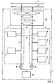
- the central unit 1 of a programmable logic controller has a control processor system 2 with an internal bus 3 and a residual processor system 4 with an internal bus 5.
- the processor systems 2, 4 are connected to an external bus system 7 via the interface module 6.
- peripheral units for. B. input modules, output modules, controller modules, etc. connected.
- the control processor system 2 has, in addition to the internal bus 3, a control processor 8 and one or more memories 9.
- the control processor system 2 may include other components, e.g. B. a coprocessor, not shown, or direct peripheral connections.
- the control processor system 2 performs all control tasks that require a real-time reaction, e.g. B. the execution of the user program, the process image transfer or alarm reactions.
- the control processor 8 is a special processor, preferably an application-specific one integrated circuit (ASIC). This allows the control processor 8 to be optimally tailored to control tasks as such and the control programming language used in particular.
- ASIC application-specific one integrated circuit
- the residual processor system 4 also has a residual processor 10.
- This residual processor 10 is preferably a standard microprocessor, e.g. B. a Siemens 80166.
- the residual processor system 4 has a RAM 11 and EPROM 12.
- a user module 13 can be coupled to the bus 5, which is designed either as a buffered RAM or as an erasable read-only memory (EPROM, EEPROM, Flash-EPROM).
- the residual processor system 4 is separate from the control processor system 2.
- the residual processor system 4 performs all tasks that are not directly connected to time-critical control tasks. These are, for example, the communication with other central units, the reloading of programs or the non-control-related data traffic with the peripheral units.
- the processor systems 2, 4 are connected to the bus system 7 via the interface module 6.
- the bus system 7 is accessed via the controllers 14, 15, which are integral components of the interface module 6.
- the interface module 6 has a lockable coupling element 16, via which the buses 3 and 5 are interconnected are connectable.
- the coupling element 16 is, for example, a tristate HCMOS driver.
- the coupling element 16 it is possible for the residual processor 10 to access the bus 3 of the control processor system 2.
- the operating system which is stored retentively in the EPROM 12, can be copied from the EPROM 12 into the memory 9 of the control processor system 2.
- the interface module 6 has a dual ported RAM 17. Both the control processor 8 and the remaining processor 10 can access the dual ported RAM 17. The processors 8, 10 can coordinate with one another by means of the dual-ported RAM 17 and the control lines 18.
- the interface module 6 is also preferably an application-specific integrated circuit (ASIC).
- ASIC application-specific integrated circuit
- the residual processor 10 When the central processing unit 1 starts up, the residual processor 10 first initializes itself. After this self-initialization, the residual processor 10, as mentioned above, copies the operating system from the EPROM 12 into the memory 9. Then the residual processor 10 triggers the control processor 8 via one of the control lines 18. so that it can initialize itself if necessary and then start processing the control program.
- the control processor 8 processes the user program.
- the residual processor 10 performs the administration and communication tasks.
- the residual processor 10 communicates, for example, with a programming device, not shown. Some The remaining processor 10 can process communication orders on its own, but for other communication orders the control processor 8 must be involved.
- the residual processor 10 stores in the dual-ported RAM 17 the data which the control processor 8 requires to process the communication job.
- the residual processor 10 then sends an interrupt signal to the control processor 8 via one of the control lines 18.
- the control processor 8 then reads out the data stored in the dual-ported RAM 17 and processes the communication job.
- the control processor 8 stores the result in the dual-ported RAM 17 and sends an interrupt signal via one of the control lines 18 to the residual processor 10.
- the residual processor 10 then reads out the result of the communication from the dual-ported RAM 17 and processes it Communication order continues.
- the control processor 8 continues the processing of the user program.
- control processor 8 In individual cases, communication can also be initiated by the control processor 8. In this case, of course, the control processor 8 first stores data in the dual-ported RAM 17 and then instructs the remaining processor 10 to execute the job via one of the interrupt lines 18.
- the user program is loaded or reloaded into the memory 9 on the initiative of the control processor 8.
- the control processor 8 stores the job in the dual-ported RAM 17 and triggers the remaining processor 10 via one of the lines 18.
- the residual processor 10 reads part of the requested user program from the user module 13 and stores this part in the dual ported RAM 17.
- An interrupt signal is then again transmitted from the residual processor 10 to the control processor 8 via one of the control lines 18.
- the control processor 8 then reads out the dual ported RAM 17 and stores the data in the memory 9. This process is repeated until the entire requested user program has been transferred to the memory 9.
- the user program influences the residual processor 10 only insofar as the residual processor 10 receives standardized, tested orders from the control processor 8. Errors in the user program can therefore not lead to malfunctions of the residual processor 10.
- the residual processor 10 is thereby able to monitor the central unit 1 including the control processor system 2.
- the residual processor system 4 can thus be configured as a master system for monitoring the central unit 1.
- the bus system 7 is divided into two sub-buses 7 ', 7''.
- the partial bus 7 ′ is a control bus and is connected to the controller 14, which is connected to the control processor system 2.
- the bus 7 ′′ is a residual bus and is connected to the controller 15, which is connected to the residual processor system 4.
- the residual processor system 4 can also be connectable to the control bus 7 ′ and the control processor system 2 also to the residual bus 7 ′′ for special tasks.
- the embodiment according to FIG. 2 can only be used with newly designed bus systems 7.
- the controllers 14, 15 ensure that the bus system 7 is separated from the internal buses 3, 5.
- the processor systems 2, 4 can therefore be developed independently of the structure of the bus system 7, for example as 32-bit systems, even if the bus system 7 is an 8-bit system.
- the processor systems 2, 4 can also be operated independently of the bus system 7, for example at 20 MHz, even if accesses to the bus system 7 take considerably longer. Any necessary intermediate storage or buffering of data is carried out by the controllers 14, 15.
- FIG. 2 also shows a further improvement of the invention, which can in principle be used in both embodiments.
- the memory 9 of the control processor system 2 is split into two partial memories 9 ', 9' '.
- the partial memory 9 ′′ is connected to both processor systems 2, 4 via bidirectional, lockable coupling elements 19, typically HCMOS drivers.
- HCMOS drivers typically HCMOS drivers.
- the interface module 6 can have a third controller 20, which is connected to the two processor systems 2, 4.
- the controller 20 is preferably also integrated in the interface module 6. The necessary residual communication between the control processor system 2 and the residual processor system 4 can be handled even more efficiently by means of the controller 20.
Landscapes
- Physics & Mathematics (AREA)
- General Physics & Mathematics (AREA)
- Engineering & Computer Science (AREA)
- Automation & Control Theory (AREA)
- Multi Processors (AREA)
- Control By Computers (AREA)
- Feedback Control In General (AREA)
- Programmable Controllers (AREA)
Priority Applications (6)
| Application Number | Priority Date | Filing Date | Title |
|---|---|---|---|
| DE59206826T DE59206826D1 (de) | 1992-09-28 | 1992-09-28 | Prozesssteuerungssystem |
| AT92116560T ATE140805T1 (de) | 1992-09-28 | 1992-09-28 | Prozesssteuerungssystem |
| EP92116560A EP0590175B1 (fr) | 1992-09-28 | 1992-09-28 | Système de commande de processus |
| CA002106899A CA2106899A1 (fr) | 1992-09-28 | 1993-09-24 | Unite centrale de systeme de controle-commande de procede |
| JP5261930A JP2778015B2 (ja) | 1992-09-28 | 1993-09-24 | プロセス制御システム |
| US08/127,924 US6184904B1 (en) | 1992-09-28 | 1993-09-28 | Central processing unit for a process control system |
Applications Claiming Priority (1)
| Application Number | Priority Date | Filing Date | Title |
|---|---|---|---|
| EP92116560A EP0590175B1 (fr) | 1992-09-28 | 1992-09-28 | Système de commande de processus |
Publications (2)
| Publication Number | Publication Date |
|---|---|
| EP0590175A1 true EP0590175A1 (fr) | 1994-04-06 |
| EP0590175B1 EP0590175B1 (fr) | 1996-07-24 |
Family
ID=8210065
Family Applications (1)
| Application Number | Title | Priority Date | Filing Date |
|---|---|---|---|
| EP92116560A Expired - Lifetime EP0590175B1 (fr) | 1992-09-28 | 1992-09-28 | Système de commande de processus |
Country Status (6)
| Country | Link |
|---|---|
| US (1) | US6184904B1 (fr) |
| EP (1) | EP0590175B1 (fr) |
| JP (1) | JP2778015B2 (fr) |
| AT (1) | ATE140805T1 (fr) |
| CA (1) | CA2106899A1 (fr) |
| DE (1) | DE59206826D1 (fr) |
Cited By (5)
| Publication number | Priority date | Publication date | Assignee | Title |
|---|---|---|---|---|
| US5621672A (en) * | 1993-04-06 | 1997-04-15 | Honda Giken Kogyo Kabushiki Kaisha | Multitask control system |
| EP0698837B1 (fr) * | 1994-08-12 | 1997-04-23 | Siemens Aktiengesellschaft | Procédé et appareil de transfert de données périodique avec fonction de diffusion pour un échange indépendant de données entre unités périphériques externes |
| WO1999035543A1 (fr) * | 1998-01-07 | 1999-07-15 | Continental Teves Ag & Co. Ohg | Dispositif numerique electronique |
| WO1999038055A1 (fr) * | 1998-01-24 | 1999-07-29 | Dr. Johannes Heidenhain Gmbh | Procede et circuit pour controler des parametres machine |
| WO2006002695A1 (fr) * | 2004-07-06 | 2006-01-12 | Daimlerchrysler Ag | Systeme redondant de bus de donnees |
Families Citing this family (5)
| Publication number | Priority date | Publication date | Assignee | Title |
|---|---|---|---|---|
| JP3478990B2 (ja) * | 1999-04-09 | 2003-12-15 | 山形日本電気株式会社 | 生産支援システムとその制御方法並びにその方法を記録した記録媒体 |
| US7024495B2 (en) * | 2001-03-30 | 2006-04-04 | Omron Corporation | Programmable controller |
| ES2246725B1 (es) * | 2004-08-13 | 2007-05-01 | K-Lon Control, S.A. | Sistema domotico aplicable a entornos con un elevado numero de señales. |
| US9146865B2 (en) * | 2005-01-26 | 2015-09-29 | Lantiq Beteiligungs-GmbH & Co.KG | Operating a dual-ported internal memory |
| US7673126B2 (en) * | 2006-09-19 | 2010-03-02 | Intel Corporation | Methods and apparatus to self-initialize a processor |
Citations (3)
| Publication number | Priority date | Publication date | Assignee | Title |
|---|---|---|---|---|
| EP0088805A1 (fr) * | 1981-09-22 | 1983-09-21 | Fanuc Ltd. | Controleur de sequence programmable |
| GB2250106A (en) * | 1990-08-27 | 1992-05-27 | Toshiba Kk | Operation control device for washing machines |
| EP0496097A2 (fr) * | 1990-12-26 | 1992-07-29 | Allen-Bradley Company, Inc. | Processeur d'automate programmable pour l'exécution concourant d'un multiple de programmes de commande d'utilisateurs |
Family Cites Families (23)
| Publication number | Priority date | Publication date | Assignee | Title |
|---|---|---|---|---|
| US3676861A (en) * | 1970-12-30 | 1972-07-11 | Honeywell Inf Systems | Multiple mask registers for servicing interrupts in a multiprocessor system |
| US3812469A (en) * | 1972-05-12 | 1974-05-21 | Burroughs Corp | Multiprocessing system having means for partitioning into independent processing subsystems |
| US4065809A (en) * | 1976-05-27 | 1977-12-27 | Tokyo Shibaura Electric Co., Ltd. | Multi-processing system for controlling microcomputers and memories |
| IT1071840B (it) * | 1976-11-12 | 1985-04-10 | Olivetti & Co Spa | Sistema multiprocessore per la commutazione automatica di linee telegrafiche e metodo di trasferimento dei caratteri di informazione |
| US4200930A (en) * | 1977-05-23 | 1980-04-29 | Burroughs Corporation | Adapter cluster module for data communications subsystem |
| US4495569A (en) * | 1982-06-28 | 1985-01-22 | Mitsubishi Denki Kabushiki Kaisha | Interrupt control for multiprocessor system with storage data controlling processor interrupted by devices |
| US4654654A (en) * | 1983-02-07 | 1987-03-31 | At&T Bell Laboratories | Data network acknowledgement arrangement |
| JPS59165119A (ja) * | 1983-03-11 | 1984-09-18 | Hitachi Ltd | 入出力制御装置 |
| US4713758A (en) * | 1985-04-29 | 1987-12-15 | American Telephone And Telegraph Company, At&T Bell Laboratories | Computer testing arrangement |
| US4907070A (en) * | 1985-10-17 | 1990-03-06 | Ampex Corporation | Time base corrector with memory mapped system control |
| JP2834122B2 (ja) * | 1987-07-08 | 1998-12-09 | 株式会社日立製作所 | 制御装置 |
| JPH01161505A (ja) * | 1987-12-18 | 1989-06-26 | Hitachi Ltd | プロセスコントローラの実時間管理装置 |
| JPH0219901A (ja) * | 1988-07-08 | 1990-01-23 | Yaskawa Electric Mfg Co Ltd | アナログ出力方法とその装置 |
| JPH0275002A (ja) * | 1988-09-10 | 1990-03-14 | Fujitsu Ltd | ディジタル制御装置 |
| JPH07120292B2 (ja) * | 1989-06-19 | 1995-12-20 | 日本電気株式会社 | 情報処理システム |
| US5131092A (en) * | 1989-09-01 | 1992-07-14 | Square D Company | Communication system enabling programmable logic controllers access to host computer tasks and host computer access to programmable logic controllers without polling |
| WO1991004540A1 (fr) * | 1989-09-08 | 1991-04-04 | Auspex Systems, Inc. | Architecture d'un systeme d'exploitation comprenant plusieurs unites de traitement |
| KR940001878B1 (ko) * | 1990-03-08 | 1994-03-10 | 가부시끼가이샤 히다찌세이사꾸쇼 | 멀티 프로세서시스템 및 인터럽션 제어장치 |
| US5222213A (en) * | 1990-04-10 | 1993-06-22 | At&T Bell Laboratories | Low-cost display controller comprising a DMA or communications controller operating under processor control |
| FR2665810B1 (fr) * | 1990-08-09 | 1993-06-18 | Bull Sa | Controleur de communication entre un ordinateur et une pluralite de terminaux de type rnis. |
| JP2863295B2 (ja) * | 1990-10-04 | 1999-03-03 | 沖電気工業株式会社 | 通信機能付き情報処理装置 |
| CA2067599A1 (fr) * | 1991-06-10 | 1992-12-11 | Bruce Alan Smith | Ordinateur personnel a connecteur pour bus maitre auxiliaire |
| US5325120A (en) * | 1991-11-15 | 1994-06-28 | Kuehnle Manfred R | Electrostatic reproduction apparatus having a dielectric ink-phobic imaging member and field-emission write head |
-
1992
- 1992-09-28 AT AT92116560T patent/ATE140805T1/de not_active IP Right Cessation
- 1992-09-28 EP EP92116560A patent/EP0590175B1/fr not_active Expired - Lifetime
- 1992-09-28 DE DE59206826T patent/DE59206826D1/de not_active Expired - Lifetime
-
1993
- 1993-09-24 JP JP5261930A patent/JP2778015B2/ja not_active Expired - Fee Related
- 1993-09-24 CA CA002106899A patent/CA2106899A1/fr not_active Abandoned
- 1993-09-28 US US08/127,924 patent/US6184904B1/en not_active Expired - Lifetime
Patent Citations (3)
| Publication number | Priority date | Publication date | Assignee | Title |
|---|---|---|---|---|
| EP0088805A1 (fr) * | 1981-09-22 | 1983-09-21 | Fanuc Ltd. | Controleur de sequence programmable |
| GB2250106A (en) * | 1990-08-27 | 1992-05-27 | Toshiba Kk | Operation control device for washing machines |
| EP0496097A2 (fr) * | 1990-12-26 | 1992-07-29 | Allen-Bradley Company, Inc. | Processeur d'automate programmable pour l'exécution concourant d'un multiple de programmes de commande d'utilisateurs |
Non-Patent Citations (1)
| Title |
|---|
| IEEE TRANSACTIONS ON VEHICULAR TECHNOLOGY Bd. 39, Nr. 3, 1990, NEW YORK, US Seiten 271 - 276 KAMAL N. MAJEED 'Dual-Processor Controller with Vehicle Suspension Applications' * |
Cited By (8)
| Publication number | Priority date | Publication date | Assignee | Title |
|---|---|---|---|---|
| US5621672A (en) * | 1993-04-06 | 1997-04-15 | Honda Giken Kogyo Kabushiki Kaisha | Multitask control system |
| DE4411426B4 (de) * | 1993-04-06 | 2004-07-01 | Honda Giken Kogyo K.K. | Multitask-Steuersystem |
| EP0698837B1 (fr) * | 1994-08-12 | 1997-04-23 | Siemens Aktiengesellschaft | Procédé et appareil de transfert de données périodique avec fonction de diffusion pour un échange indépendant de données entre unités périphériques externes |
| WO1999035543A1 (fr) * | 1998-01-07 | 1999-07-15 | Continental Teves Ag & Co. Ohg | Dispositif numerique electronique |
| US6502019B1 (en) | 1998-01-07 | 2002-12-31 | Continental Teves Ag & Co., Ohg | Electronic digital device employing fault detection |
| WO1999038055A1 (fr) * | 1998-01-24 | 1999-07-29 | Dr. Johannes Heidenhain Gmbh | Procede et circuit pour controler des parametres machine |
| US6618637B1 (en) | 1998-01-24 | 2003-09-09 | Dr. Johannes Heidenhain Gmbh | Method and circuit configuration for monitoring machine parameters |
| WO2006002695A1 (fr) * | 2004-07-06 | 2006-01-12 | Daimlerchrysler Ag | Systeme redondant de bus de donnees |
Also Published As
| Publication number | Publication date |
|---|---|
| US6184904B1 (en) | 2001-02-06 |
| EP0590175B1 (fr) | 1996-07-24 |
| DE59206826D1 (de) | 1996-08-29 |
| CA2106899A1 (fr) | 1994-03-29 |
| JP2778015B2 (ja) | 1998-07-23 |
| JPH06222810A (ja) | 1994-08-12 |
| ATE140805T1 (de) | 1996-08-15 |
Similar Documents
| Publication | Publication Date | Title |
|---|---|---|
| DE69320122T2 (de) | Speicherprogrammierbare Steuerung mit Leiterdiagramm-Makroinstrucktionen | |
| DE3876780T2 (de) | Mikrorechner mit eingebauter chipauswahl und programmierbarer busdehnung. | |
| DE3685876T2 (de) | Meister-sklave-mikroprozessorsystem mit einem virtuellen speicher. | |
| EP0655682B1 (fr) | Unité arithmétique avec plusieures tâches | |
| DE69023018T2 (de) | Prozessor-Unterbrechungssteuerung. | |
| EP0636956B1 (fr) | Méthode de chargement de données | |
| EP0057756B1 (fr) | Dispositif pour un échange de données dans des systèmes de multi-microcalculateur operant en parallèle | |
| DE2744531A1 (de) | Elektronische datenverarbeitungsanlage | |
| EP0050304A1 (fr) | Système multiprocesseur avec détermination du processeur obtenant le résultat le plus faible | |
| EP0121037B1 (fr) | Commande à programme mémorisé | |
| EP0590175B1 (fr) | Système de commande de processus | |
| DE102013113262A1 (de) | Auslöser-Leitwegeinheit | |
| EP0050305B1 (fr) | Dispositif pour la commande d'accès de processeurs sur une ligne de données | |
| DE69229851T2 (de) | Sequentielles Urladesystem | |
| DE69622785T2 (de) | Prozessorunterbrechungssteuerung | |
| DE3750045T2 (de) | Unterbrechungssteuerungsvorrichtung für eine virtuelle Maschine mit einer Vielzahl von Verarbeitungseinheiten. | |
| DE2533737A1 (de) | Datenprozessor | |
| DE4223454A1 (de) | Datenuebertragungssystem fuer eine digitale signalverarbeitungsvorrichtung | |
| DE69600364T2 (de) | Vorrichtung zur Inbetriebnahme einer Halbleiterschaltung | |
| DE10213860B4 (de) | Programmierbare Steuerung | |
| DE2657897A1 (de) | Externes geraet, das die ureingabe fest gespeichert enthaelt, fuer elektronische datenverarbeitungsanlagen mit einem zentralen speicher | |
| EP0465793A2 (fr) | Système à multiprocesseur pour dispositif de commande et de diagnostic dans un véhicule | |
| DE2932394A1 (de) | Intelligente, programmierbare prozessteueranordnung | |
| EP1283471B1 (fr) | Unité commandée par programme | |
| DE102006052757A1 (de) | Automatisierungsgerät mit einer Verarbeitungseinheit und Verwendung einer Verarbeitungseinheit in einem Automatisierungsgerät |
Legal Events
| Date | Code | Title | Description |
|---|---|---|---|
| PUAI | Public reference made under article 153(3) epc to a published international application that has entered the european phase |
Free format text: ORIGINAL CODE: 0009012 |
|
| AK | Designated contracting states |
Kind code of ref document: A1 Designated state(s): AT CH DE FR GB IT LI NL SE |
|
| 17P | Request for examination filed |
Effective date: 19940419 |
|
| 17Q | First examination report despatched |
Effective date: 19950811 |
|
| GRAG | Despatch of communication of intention to grant |
Free format text: ORIGINAL CODE: EPIDOS AGRA |
|
| GRAH | Despatch of communication of intention to grant a patent |
Free format text: ORIGINAL CODE: EPIDOS IGRA |
|
| GRAH | Despatch of communication of intention to grant a patent |
Free format text: ORIGINAL CODE: EPIDOS IGRA |
|
| GRAA | (expected) grant |
Free format text: ORIGINAL CODE: 0009210 |
|
| AK | Designated contracting states |
Kind code of ref document: B1 Designated state(s): AT CH DE FR GB IT LI NL SE |
|
| PG25 | Lapsed in a contracting state [announced via postgrant information from national office to epo] |
Ref country code: IT Free format text: LAPSE BECAUSE OF FAILURE TO SUBMIT A TRANSLATION OF THE DESCRIPTION OR TO PAY THE FEE WITHIN THE PRE;WARNING: LAPSES OF ITALIAN PATENTS WITH EFFECTIVE DATE BEFORE 2007 MAY HAVE OCCURRED AT ANY TIME BEFORE 2007. THE CORRECT EFFECTIVE DATE MAY BE DIFFERENT FROM THE ONE RECORDED.SCRIBED TIME-LIMIT Effective date: 19960724 Ref country code: NL Free format text: LAPSE BECAUSE OF FAILURE TO SUBMIT A TRANSLATION OF THE DESCRIPTION OR TO PAY THE FEE WITHIN THE PRESCRIBED TIME-LIMIT Effective date: 19960724 |
|
| REF | Corresponds to: |
Ref document number: 140805 Country of ref document: AT Date of ref document: 19960815 Kind code of ref document: T |
|
| REG | Reference to a national code |
Ref country code: CH Ref legal event code: NV Representative=s name: SIEMENS SCHWEIZ AG |
|
| REF | Corresponds to: |
Ref document number: 59206826 Country of ref document: DE Date of ref document: 19960829 |
|
| GBT | Gb: translation of ep patent filed (gb section 77(6)(a)/1977) |
Effective date: 19960830 |
|
| PG25 | Lapsed in a contracting state [announced via postgrant information from national office to epo] |
Ref country code: SE Effective date: 19961024 |
|
| ET | Fr: translation filed | ||
| NLV1 | Nl: lapsed or annulled due to failure to fulfill the requirements of art. 29p and 29m of the patents act | ||
| PLBE | No opposition filed within time limit |
Free format text: ORIGINAL CODE: 0009261 |
|
| 26N | No opposition filed | ||
| REG | Reference to a national code |
Ref country code: GB Ref legal event code: IF02 |
|
| PGFP | Annual fee paid to national office [announced via postgrant information from national office to epo] |
Ref country code: CH Payment date: 20031203 Year of fee payment: 12 |
|
| PGFP | Annual fee paid to national office [announced via postgrant information from national office to epo] |
Ref country code: AT Payment date: 20040831 Year of fee payment: 13 |
|
| PG25 | Lapsed in a contracting state [announced via postgrant information from national office to epo] |
Ref country code: CH Free format text: LAPSE BECAUSE OF NON-PAYMENT OF DUE FEES Effective date: 20040930 Ref country code: LI Free format text: LAPSE BECAUSE OF NON-PAYMENT OF DUE FEES Effective date: 20040930 |
|
| REG | Reference to a national code |
Ref country code: CH Ref legal event code: PL |
|
| PG25 | Lapsed in a contracting state [announced via postgrant information from national office to epo] |
Ref country code: AT Free format text: LAPSE BECAUSE OF NON-PAYMENT OF DUE FEES Effective date: 20050928 |
|
| PGFP | Annual fee paid to national office [announced via postgrant information from national office to epo] |
Ref country code: DE Payment date: 20101119 Year of fee payment: 19 |
|
| PGFP | Annual fee paid to national office [announced via postgrant information from national office to epo] |
Ref country code: GB Payment date: 20110915 Year of fee payment: 20 Ref country code: FR Payment date: 20111005 Year of fee payment: 20 |
|
| REG | Reference to a national code |
Ref country code: DE Ref legal event code: R071 Ref document number: 59206826 Country of ref document: DE |
|
| REG | Reference to a national code |
Ref country code: DE Ref legal event code: R071 Ref document number: 59206826 Country of ref document: DE |
|
| REG | Reference to a national code |
Ref country code: GB Ref legal event code: PE20 Expiry date: 20120927 |
|
| PG25 | Lapsed in a contracting state [announced via postgrant information from national office to epo] |
Ref country code: DE Free format text: LAPSE BECAUSE OF EXPIRATION OF PROTECTION Effective date: 20120929 Ref country code: GB Free format text: LAPSE BECAUSE OF EXPIRATION OF PROTECTION Effective date: 20120927 |