EP0590831B1 - Circuits de séparation des signaux luminance/chrominance - Google Patents
Circuits de séparation des signaux luminance/chrominance Download PDFInfo
- Publication number
- EP0590831B1 EP0590831B1 EP93307330A EP93307330A EP0590831B1 EP 0590831 B1 EP0590831 B1 EP 0590831B1 EP 93307330 A EP93307330 A EP 93307330A EP 93307330 A EP93307330 A EP 93307330A EP 0590831 B1 EP0590831 B1 EP 0590831B1
- Authority
- EP
- European Patent Office
- Prior art keywords
- signal
- circuit
- output
- filter means
- level
- Prior art date
- Legal status (The legal status is an assumption and is not a legal conclusion. Google has not performed a legal analysis and makes no representation as to the accuracy of the status listed.)
- Expired - Lifetime
Links
Images


Classifications
-
- H—ELECTRICITY
- H04—ELECTRIC COMMUNICATION TECHNIQUE
- H04N—PICTORIAL COMMUNICATION, e.g. TELEVISION
- H04N9/00—Details of colour television systems
- H04N9/77—Circuits for processing the brightness signal and the chrominance signal relative to each other, e.g. adjusting the phase of the brightness signal relative to the colour signal, correcting differential gain or differential phase
- H04N9/78—Circuits for processing the brightness signal and the chrominance signal relative to each other, e.g. adjusting the phase of the brightness signal relative to the colour signal, correcting differential gain or differential phase for separating the brightness signal or the chrominance signal from the colour television signal, e.g. using comb filter
Definitions
- This invention relates to luminance and chrominance signal separation circuits.
- EP-A-0 412 790 discloses an adaptive comb filter for separating at least one component of a video signal which includes a filter input for receiving the video signal, a first delay device for delaying the video signal by a first interval to produce a first delayed video signal, a second delay device for delaying the video signal by a second interval to produce a second delayed video signal, a first signal subtracter for producing a first difference signal proportional to a difference between the video signal and the first delayed video signal, a second subtracter for producing a second difference signal proportional to a difference between the first delayed video signal and the second delayed video signal, a first signal summing device for producing a first summation signal proportional to a summation of the first difference signal and the second difference signal, a signal selecting device for controllably selecting one of the first difference signal, the second difference signal and the first summation signal as the separated component of the video signal, a second summing device for producing a second summation signal proportional to a summation of the video signal and the
- a luminance/chrominance (Y/V) separation circuit using a comb filter for separating a composite video signal into a luminance signal and a chrominance signal is known, for example, from Japanese Patent Application No 2-137081.
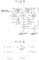
- FIG. 5 of the accompanying drawing shows a previously proposed Y/C separation circuit using a comb filter.
- a 1H (a period of one horizontal synchronization signal, or, briefly, one horizontal scanning period) delay line 4F outputs a composite video signal b obtained by delaying an input composite video signal applied thereto by one horizontal scanning period, while a 1H delay line 4S outputs a composite video signal c obtained by delaying the composite video signal b output from the 1H delay line 4F by one horizontal scanning period.
- the input composite video signal a, the composite video signal b output from the 1H delay line 4F, and the composite video signal c output from the 1H delay line 4S correspond to the composite video signals for first, second, and third horizontal lines.
- a bandpass filter (BPF) 6 extracts a signal d as a high-frequency component of the input composite video signal a.
- a bandpass filter 8 extracts a signal e as a high-frequency component of the composite video signal b output from the 1H delay line 4F.
- a bandpass filter 10 extracts a signal f as a high-frequency component of the composite video signal c output from the 1H delay line 4S.
- a subtractor 122 subtracts the output signal d of the BPF 6 from the output signal e of the BPF 8, and a 1/2 (multiply by a half) circuit 124 outputs a signal g obtained by halving the output of the subtractor 122.
- a subtractor 142 subtracts the output signal f of the BPF 10 from the output signal e of the BPF 8, and a 1/2 circuit 144 outputs a signal h obtained by halving the output of the subtractor 142.
- An adder 162 adds up the signal g and the signal h, and a 1/2 circuit 164 outputs a signal obtained by halving the output signal of the adder 162, i.e., a chrominance signal i.
- a subtractor 170 subtracts the chrominance signal i from the composite video signal b output from the 1H delay line 4F and outputs the difference as a luminance signal j.
- a circuit for separating the luminance and chrominance components of a composite video signal comprising: first delay means having an input for receiving the composite video signal; second delay means connected to said first delay means serially; first band-pass filter means connected to an input of said first delay means; second band-pass filter means connected to an input of said second delay means; third band-pass filter means connected to an output of said second delay means; the first, second and third band pass filter means each being for extracting from the composite video signal the chrominance component and the portion of the luminance component within the pass-band of the filter means; first comb filter means connected to an output of said first filter means and an output of said second filter means; second comb filter means connected to the output of said second filter means and an output of said third filter means; third comb filter means connected to an output of said first comb filter means and an output of said second comb filter means; the first, second and third comb filter means being for separating the chrominance component from the said portion of the luminance component;
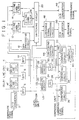
- FIG. 1 shows a structure of an embodiment of a Y/C separation circuit of the present invention.
- An input composite video signal is converted into a digital signal by an A/D converter 2.
- a delay line unit 4 is formed of a 1H delay line 4F and a 1H delay line 4S.
- the 1H delay line 4F outputs a composite video signal obtained by delaying the digitized composite video signal by one horizontal scanning period
- the 1H delay line 4S outputs a composite video signal obtained by delaying the composite video signal output from the 1H delay line 4F by one horizontal scanning period.
- the input composite video signal, the composite video signal output from the 1H delay line 4f, and the composite video signal output from the 1H delay line 4S correspond to the composite video signal for the first, second, and third horizontal lines.
- a BPF 6 extracts a signal of chrominance frequency band, i.e., a signal of high-frequency component, from the input composite video signal.
- a BPF 8 extracts a signal of chrominance frequency band, i.e., a signal of high-frequency component, from the composite video signal output from the 1H delay line 4F.
- a BPF 10 extracts a signal of chrominance frequency band, i.e., a signal of high-frequency component, from the composite video signal output from the 1H delay line 4S.
- the comb filter means of the embodiment shown in FIG. 1 is formed of 2-line comb filters 12 and 14 and a 3-line comb filter 16.
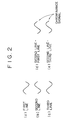
- the 2-line comb filter 12 receiving the output signal of the BPF 6 and the output signal of the BPF 8, subtracts the output signal of the BPF 6, i.e., the composite video signal for the first horizontal line (refer to FIG. 2(a)), from the output signal of the BPF 8, i.e., the composite video signal for the second horizontal line (refer to FIG. 2(b)), and outputs a chrominance signal (refer to FIG. 2(d)).
- the 2-line comb filter 14 receiving the output signal of the BPF 8 and the output signal of the BPF 10, subtracts the output signal of the BPF 10, i.e., the composite video signal for the third horizontal line (refer to FIG. 2(c)), from the output signal of the BPF 8, i.e., the composite video signal for the second horizontal line (refer to FIG. 2(b)), and outputs a chrominance signal (refer to FIG. 2(e)). Since the phase of the composite signal is inverted every line as shown in FIGs. 2(a), (b), and (c), the chrominance signal is obtained by the above described subtraction.
- the 3-line comb filter 16 adds up the output signals of the 2-line comb filters 12 and 14 and outputs a chrominance signal. By the addition, signal components other than the chrominance signal are eliminated.
- a BPF processing circuit 18 extracts a signal of a predetermined frequency band from the output signal of the BPF 8 to thereby output a chrominance signal.
- the frequency band for the BPF processing circuit 18 is selected to be an appropriate band not producing errors due to a sweep signal and the like. As described above, there are generated four types of chrominance signals in the embodiment of FIG. 1.
- a level detection unit LD detects the level of a high-frequency component of the luminance signal included in the composite video signal.
- the level detection unit LD is formed of a first level detecting portion for detecting the level of the high-frequency component of the luminance signal in the composite video signal for the first and second horizontal lines and a second level detecting portion for detecting the level of the high-frequency component of the luminance signal in the composite video signal for the second and third horizontal lines.
- the first level detecting portion includes an adder 22 for adding up the output signal of the BPF 6, i.e., the signal for the first line of the composite video signal (refer to FIG. 3(a) or (c)), and the output signal of the BPF 8, i.e., the signal for the second line of the composite video signal (refer to FIG. 3(b) or (d)), an absolute circuit 24 for obtaining an absolute value of the output of the adder 22 (refer to FIG. 3(e) (when the high-frequency component is present in the luminance signal) or refer to FIG. 3(f) (when the high-frequency component is absent in the luminance signal)), and an LPF 26 for applying a low-pass filtering (LPF) treatment to the output signal of the absolute circuit 24.
- LPF low-pass filtering
- the second level detecting portion includes an adder 28 for adding up the output signal of the BPF 8, i.e., the signal for the second line of the composite video signal, and the output signal of the BPF 10, i.e., the signal for the third line of the composite video signal, an absolute circuit 30 for obtaining an absolute value of the output of the adder 28, and an LPF 32 for applying a low-pass filtering (LPF) treatment to the output signal of the absolute circuit 30.
- LPF low-pass filtering
- a comparing circuit 34 receiving the output signals of the LPFs 26 and 32, i.e., the level of the high-frequency signal component of the luminance signal in the composite video signal for the first and second lines and the level of the high-frequency signal component of the luminance signal in the composite video signal for the second and third lines, outputs a select signal M of the 2-line comb filter 12 (refer to M in FIG. 4), a select signal N of the 2-line comb filter 14 (refer to N in FIG. 4), a select signal O of the 3-line comb filter 16 (refer to O in FIG. 4), or a select signal P of the BPF processing circuit 18 (refer to P in FIG. 4).
- a comparing unit CC shown in FIG. 1 and FIG. 4, includes comparing circuits 36 and 38 and a switch circuit 40 (denoted by reference numeral 52 in FIG. 4).
- the comparing circuit 36 decides whether or not the level of the high-frequency signal component of the luminance signal in the composite video signal for the first and second horizontal lines is lower than a predetermined comparison level.
- the comparing circuit 38 decides whether or not the level of the high-frequency signal component of the luminance signal in the composite video signal for the second and third horizontal lines is lower than a predetermined comparison level.
- a switch circuit 40 receiving the results of comparison from the comparing circuits 36 and 38, when the level of the high-frequency signal component of the luminance signal for the first and second horizontal lines is lower than the predetermined level and when the level of the high-frequency signal component of the luminance signal for the second and third horizontal lines is lower than the predetermined level, outputs an instruction to select the chrominance signal output from the BPF processing circuit 18 (i.e., an instruction to select the trap filter).
- the switch circuit 40 When at least one of the level of the high-frequency signal component of the luminance signal for the first and second horizontal lines and the level of the high-frequency signal component of the luminance signal for the second and third horizontal lines is higher than the predetermined level, the switch circuit 40 outputs an enable signal to allow the select signal output from the comparing circuit 34 as it is to be accepted.
- a switching control circuit 44 which is denoted in FIG. 4 by reference numerals 62, 64, 66, 68, 72, 74, 76, and 78, is supplied with outputs of the comparing circuit 34 and the switch circuit 40.
- the switching control circuit 44 When the switch circuit 40 has output an instruction to select the chrominance signal output from the BPF processing circuit 18, the switching control circuit 44 outputs an instruction signal to a switching circuit 20 such that the BPF processing circuit 18 is selected.
- the switch circuit 40 has output the enable signal, the content of the 2-line comb filter 12 select signal M, the 2-line comb filter 14 select signal N, the 3-line comb filter 16 select signal O, or the BPF processing circuit 18 select signal P as it is is output to the switching circuit 20.
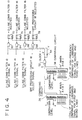
- FIG. 4 shows an example of structure of the comparing circuits 36 and 38, the switch circuit 40, and the switching control circuit 44 in the embodiment of FIG. 1.
- the switch circuit 40 is formed of a NAND gate 52 and an inverter 54
- the switching control circuit 44 is formed of NAND gates 62, 64, and 66, a NOR gate 68, and D flip-flops 72, 74, 76, and 78.
- the comparing circuit 36 determines whether or not an 8-bit input A indicating the level of the high-frequency signal component of the luminance signal in the composite video signal for the first and second lines is lower than an 8-bit input B indicating a predetermined comparison level.
- the output of the comparing circuit 36 is input to a second input of the NAND gate 52.
- the comparing circuit 38 determines whether or not an 8-bit input A indicating the level of the high-frequency signal component of the luminance signal in the composite video signal for the second and third lines is lower than an 8-bit input B indicating a predetermined comparison level.
- the output of the comparing circuit 38 is input to a third input of the NAND gate 52.
- the first input of the NAND gate 52 is supplied with an "H" level.
- the inputs on one side of the NAND gates 62, 64, and 66 and the NOR gate 68 are supplied with the select signal M of the 2-line comb filter 12, the select signal N of the 2-line comb filter 14, the select signal O of the 3-line comb filter 16, and the select signal P of the BPF processing circuit 18, respectively.
- the inputs on the other side of the NAND gates 62, 64, and 66 is supplied with an output X of the NAND gate 52.
- the input on the other side of the NOR gate 68 is supplied with an output Y of the inverter 54 obtained by inverting the output of the NAND gate 52.
- the outputs of the NAND gates 62, 64, and 66 and the NOR gate 68 are supplied to the D inputs of the D flip-flops 72, 74, 76, and 78, respectively.
- the Q output of any of the D flip-flops 72, 74, 76, and 78 is "L", it indicates that the corresponding 2-line comb filter 12, 2-line comb filter 14, 3-line comb filter 16, or the BPF processing circuit 18 should be selected.
- the comparing circuit 36 When the level of the high-frequency signal component of the luminance signal for the first and second lines is lower than a predetermined comparison level, for example "5", the comparing circuit 36 outputs an "H” output. When the level of the high-frequency signal component of the luminance signal for the second and third lines is lower than a predetermined comparison level, for example "5", the comparing circuit 38 outputs an "H” output. The fact that the outputs of the comparing circuits 36 and 38 are both "H" indicates that luminance signal for successive lines are flat and have no level difference therebetween.
- the outputs of the comparing circuits 36 and 38 becomes “L". Accordingly, the output X of the NAND gate 52 becomes "H” and the output Y of the inverter 54 becomes “L”. As a result, the outputs of the NAND gates 62, 64, and 66 and the NOR gate 68 come to reflect the select signal M of the 2-line comb filter 12, the select signal N of the 2-line comb filter 14, the select signal O of the 3-line comb filter 16, and the select signal P of the BPF processing circuit 18, as it is, respectively.
- the NAND gates 62, 64, and 66 and the NOR gate 68 when receiving the select signal M ("H") of the 2-line comb filter 12, the select signal N ("H") of the 2-line comb filter 14, the select signal O ("H") of the 3-line comb filter 16, and the select signal P ("H") of the BPF processing circuit 18, respectively, provide an "L” output. Accordingly, the D flip-flop 72, 74, 76, or 78 whose D input is "L” provides an "L” output.
- the switching circuit 20 selectively outputs one of the chrominance signals output from the 2-line comb filter 12, 2-line comb filter 14, 3-line comb filter 16, and the BPF processing circuit 18 corresponding to the output of the switching control circuit 44.
- a D/A converter 46 converts the chrominance signal selected by the switching circuit 20 into an analog signal and outputs this signal.
- a luminance signal processing circuit 48 subtracts the chrominance signal selected by the switching circuit 20 from the composite video signal output. from the 1-H delay line 4F and outputs the thus obtained luminance signal.
- a D/A converter 50 converts the luminance signal output from the luminance signal processing circuit 48 into an analog signal and outputs this signal.
- the chrominance signal from the BPF processing circuit 18 is selected (i.e., the trap filter is switch selected).
- the high-frequency component of the luminance signal is zero, the luminance signal is flat and has no difference between lines, and therefore, even if the chrominance signal from the BPF processing circuit 18 is selected (if the trap filter is switch selected) there is produced no deterioration in the high-frequency component of the luminance signal.
- the level of the noise is low, and therefor, by setting the comparison level in the comparing circuits 36 and 38 to an appropriate value, it is achieved to cause the chrominance signal from the BPF processing circuit 18 to be selected (the trap filter to be switch selected) only for the pixel in which the noise is present, so that the noise level is lowered by the filter, the noise is prevented from vertically expanding on the picture screen (i.e., it is prevented from spreading over other horizontal lines), and the noise frequency is reduced to 1/3.
- a comb filter is selected so that a signal deterioration is prevented from occurring.
- the NTSC carrier signal which can leak out when an NTSC signal is converted to a PAL signal in a broadcasting station, produces a low-level vertical line on the picture screen.
- Such a signal can be eliminated by setting the comparison level in the comparing circuits 36 and 38 to an appropriate value so that the chrominance signal from the BPF processing circuit 18 is selected (the trap filter is switch selected). Since such a leakage signal is contained in the same component as the luminance signal, it has been unremovable by a conventional comb filter. However, since it is of a low level, it can be removed by the above embodiment.
- the embodiment is also applicable to the PAL signal by replacing the 1-H delay lines 4F and 4S with 2-H delay lines.
- the Y/C separation circuit embodying the invention is operative such that a chrominance signal as the output of bandpass filter means is selected and output when the level of the high-frequency component of a luminance signal is lower than a predetermined level, the noise frequency can be reduced as compared with that in the Y/C separation circuit of FIG. 5 while the high-frequency component of the luminance signal is not deteriorated and the noise level is equally lowered. More specifically, when the level of the high-frequency component of the luminance signal is low, the high-frequency component is not deteriorated even if the chrominance signal is generated by means of a bandpass filter (i.e., even if a trap filter is switch selected).
- a chrominance signal when a chrominance signal is generated by means of the bandpass filter, the noise is prevented from expanding in the vertical direction, i.e., from spreading over a plurality of horizontal lines, and hence the noise frequency is reduced.
- the level of the high-frequency component of the luminance signal is high, a chrominance signal is generated by comb filter means, and therefore, no signal deterioration is produced.
- the NTSC carrier signal leaking out when an NTSC signal is converted to a PAL signal in a broadcasting station which has been unremovable by the previously proposed Y/C separation circuit, can be removed by the Y/C separation circuit embodying the invention.
Landscapes
- Engineering & Computer Science (AREA)
- Multimedia (AREA)
- Signal Processing (AREA)
- Processing Of Color Television Signals (AREA)
Claims (9)
- Circuit pour séparer la composante de luminance et de chrominance d'un signal vidéo composite, le circuit comprenant :caractérisé parun premier moyen à retard (4F) ayant une entrée pour recevoir le signal vidéo composite ;un second moyen à retard (4S) raccordé audit premier moyen à retard en série ;un premier moyen de filtre passe-bande (6) raccordé à une entrée dudit premier moyen à retard ;un second moyen de filtre passe-bande (8) raccordé à une entrée dudit second moyen à retard ;un troisième moyen de filtre passe-bande (10) raccordé à une sortie dudit second moyen à retard ;les premier, second et troisième moyens de filtre passe-bande étant chacun pour extraire à partir du signal vidéo composite la composante de chrominance et la partie de la composante de luminance dans la bande passante du moyen de filtre ;un premier moyen de filtre en peigne (12) raccordé à une sortie dudit premier moyen de filtre et une sortie dudit second moyen de filtre ;un second moyen de filtre en peigne (14) raccordé à la sortie dudit second moyen de filtre et une sortie dudit troisième moyen de filtre ;un troisième moyen de filtre en peigne (16) raccordé à une sortie dudit premier moyen de filtre en peigne et une sortie dudit second moyen de filtre en peigne ;les premier, second et troisième moyens de filtre en peigne étant pour séparer la composante de chrominance de ladite partie de la composante de luminance ;un quatrième moyen de filtre passe-bande (18) raccordé à la sortie du second moyen de filtre (8) pour séparer la composante de chrominance de ladite partie de la composante de luminance ;un circuit de commutation (20) pour sélectionner ledit premier moyen de filtre en peigne, ledit second moyen de filtre en peigne, ledit troisième moyen de filtre en peigne et ledit quatrième moyen de filtre passe-bande ; etun moyen (LD) raccordé aux sorties desdits premier (6), second (8) et troisième (10) moyens de filtre pour déterminer le niveau de ladite partie de la composante de luminance ;un moyen de comparaison (CC) pour comparer le niveau déterminé de ladite partie de la composante de luminance à un niveau de référence prédéterminé et pour commander le moyen de commutation pour sélectionner le quatrième moyen de filtre passe-bande lorsque le niveau déterminé est plus petit que le niveau de référence.
- Circuit selon la revendication 1, dans lequel ladite unité de détection de niveau (LD) comprend :un premier moyen d'additionneur (22) pour additionner les sorties des premier et second moyens de filtre ;un second moyen d'additionneur (28) pour additionner les sorties des second et troisième moyens de filtre ;un premier circuit de valeur absolue (24) pour créer une valeur absolue du signal de sortie dudit premier moyen d'additionneur (22) ;un second circuit de valeur absolue (30) pour créer une valeur absolue du signal de sortie dudit second moyen d'additionneur (28) ;un premier moyen de filtre passe-bas (26) raccordé à la sortie dudit premier circuit absolu ; etun second moyen de filtre passe-bas (32) raccordé à la sortie dudit second circuit absolu.
- Circuit selon la revendication 2, dans lequel ledit moyen de comparaison (CC) comprend :un premier circuit de comparaison (36) pour comparer le niveau de sortie dudit premier filtre passe-bas (26) audit niveau de référence prédéterminé ;un second circuit de comparaison (38) pour comparer le niveau d'une sortie dudit second filtre passe-bas (32) audit niveau de référence prédéterminé ; etun moyen de commande de commutation (40, 44) pour forcer le moyen de commutation (20) à sélectionner le quatrième moyen de filtre passe-bande lorsque les niveaux des sorties desdits filtres passe-bas sont plus petits que le niveau de référence prédéterminé.
- Circuit selon la revendication 3, comprenant en outre un troisième circuit de comparaison (34) pour comparer les sorties des premier (26) et second (32) filtres passe-bas, et le moyen de commande de commutation (40, 44) force le moyen de commutation (20) à sélectionner le premier, second et troisième filtre en peigne en fonction de la comparaison par le troisième moyen de comparaison lorsque le niveau d'au moins une des sorties des premier, second filtres passe-bas est plus grand que le niveau de référence prédéterminé.
- Circuit selon la revendication 3 ou 4, dans lequel ledit moyen de commande de commutation (40, 44) comprend une porte NON ET (52).
- Circuit selon la revendication 3, 4 ou 5, dans lequel ledit moyen de commande de commutation comprend plusieurs circuits de portes logiques (62 à 68) et plusieurs circuits de bascule (72 à 78).
- Circuit de séparation selon l'une quelconque des revendications précédentes, dans lequel le temps de retard de chacun desdits premier (4F) et second (4S) moyens à retard est une période de ligne.
- Circuit de séparation selon une quelconque des revendications précédentes, dans lequel le temps de retard de chacun desdits premier et second moyens de filtre en peigne est deux périodes de ligne et le temps de retard dudit troisième moyen de filtre en peigne est trois périodes de ligne.
- Circuit de séparation selon la revendication 8, comprenant :un moyen de convertisseur analogique-numérique (2) pour convertir le signal d'entrée dudit premier moyen à retard sous forme numérique ;un premier moyen de convertisseur numérique analogique (50) pour convertir un signal de sortie d'un circuit de traitement de signal de luminance (48) pour traiter un signal de sortie dudit circuit de commutation (20) et un signal de sortie dudit premier moyen à retard (4F) sous forme analogique ; etun second moyen de convertisseur numérique analogique (46) pour convertir un signal de sortie dudit circuit de commutation sous forme analogique.
Applications Claiming Priority (2)
| Application Number | Priority Date | Filing Date | Title |
|---|---|---|---|
| JP285177/92 | 1992-09-30 | ||
| JP28517792A JP3263791B2 (ja) | 1992-09-30 | 1992-09-30 | Yc分離回路 |
Publications (3)
| Publication Number | Publication Date |
|---|---|
| EP0590831A2 EP0590831A2 (fr) | 1994-04-06 |
| EP0590831A3 EP0590831A3 (en) | 1994-06-22 |
| EP0590831B1 true EP0590831B1 (fr) | 1999-03-17 |
Family
ID=17688101
Family Applications (1)
| Application Number | Title | Priority Date | Filing Date |
|---|---|---|---|
| EP93307330A Expired - Lifetime EP0590831B1 (fr) | 1992-09-30 | 1993-09-16 | Circuits de séparation des signaux luminance/chrominance |
Country Status (4)
| Country | Link |
|---|---|
| US (1) | US5426470A (fr) |
| EP (1) | EP0590831B1 (fr) |
| JP (1) | JP3263791B2 (fr) |
| DE (1) | DE69323947T2 (fr) |
Families Citing this family (11)
| Publication number | Priority date | Publication date | Assignee | Title |
|---|---|---|---|---|
| EP0613311A1 (fr) * | 1993-02-26 | 1994-08-31 | Kabushiki Kaisha Toshiba | Circuit de séparation Y/C |
| JP3227941B2 (ja) * | 1993-10-22 | 2001-11-12 | 松下電器産業株式会社 | 色度信号分離装置 |
| JP3149677B2 (ja) * | 1994-04-21 | 2001-03-26 | 松下電器産業株式会社 | Y/c分離装置 |
| JPH09224260A (ja) * | 1996-02-19 | 1997-08-26 | Matsushita Electric Ind Co Ltd | Y/c分離装置 |
| DE19609193A1 (de) * | 1996-03-09 | 1997-09-11 | Thomson Brandt Gmbh | Verfahren und Schaltungsanordnung zum Trennen von Luminanz- und Chrominanzsignalen eines FBAS-Signals |
| MY123791A (en) * | 1996-11-01 | 2006-06-30 | Matsushita Electric Industrial Co Ltd | 2- line yc separation device |
| JP3500883B2 (ja) * | 1996-12-12 | 2004-02-23 | 松下電器産業株式会社 | カラー方式判別回路 |
| TWI280062B (en) * | 2005-10-13 | 2007-04-21 | Realtek Semiconductor Corp | Signal separation apparatus applied in image transmission system and related method |
| TWI347118B (en) * | 2006-02-14 | 2011-08-11 | Realtek Semiconductor Corp | Image processing device and method |
| TWI339527B (en) * | 2006-02-15 | 2011-03-21 | Realtek Semiconductor Corp | Method and apparatus for enhancing image quality |
| JP2008175845A (ja) * | 2007-01-16 | 2008-07-31 | Fujitsu Ten Ltd | 表示制御装置及び表示装置 |
Family Cites Families (13)
| Publication number | Priority date | Publication date | Assignee | Title |
|---|---|---|---|---|
| NL8403487A (nl) * | 1984-11-15 | 1986-06-02 | Stamicarbon | Werkwijze voor de enzymatische scheiding van dl-alfa-aminozuuramides. |
| US4845547A (en) * | 1988-03-28 | 1989-07-04 | North American Philips Corporation | Non-linear comb filter for color TV receivers |
| JPH0271693A (ja) * | 1988-09-06 | 1990-03-12 | Sony Corp | 輝度/クロマ分離回路 |
| DE3836043A1 (de) * | 1988-10-20 | 1990-04-26 | Thomson Brandt Gmbh | Schaltung fuer ein adaptives kammfilter zur trennung von leuchtdichtesignal und farbartsignal eines fbas-pal-signals |
| JPH0720265B2 (ja) * | 1988-11-04 | 1995-03-06 | 三菱電機株式会社 | 映像信号処理回路 |
| JPH0366287A (ja) * | 1989-08-04 | 1991-03-20 | Matsushita Electric Ind Co Ltd | 信号分離装置 |
| US5093715A (en) * | 1989-08-10 | 1992-03-03 | Sony Corporation | Adaptive comb filter for separating at least one component of a video signal |
| US5016092A (en) * | 1989-11-17 | 1991-05-14 | Rca Licensing Corporation | Control circuitry for an adaptive multistandard video comb filter |
| KR910013951A (ko) * | 1989-12-12 | 1991-08-08 | 이헌조 | 복합영상신호의 휘도/색도신호 분리회로 |
| KR0170630B1 (ko) * | 1990-06-20 | 1999-03-20 | 강진구 | 휘도/색신호 전처리장치 |
| KR930003177B1 (ko) * | 1990-06-29 | 1993-04-23 | 삼성전자 주식회사 | 휘도신호와 색신호 분리용 패턴 적응형 디지탈 콤 필터 |
| KR930008184B1 (ko) * | 1990-06-30 | 1993-08-26 | 삼성전자 주식회사 | 휘도/색신호 분리 회로 |
| DE4106076A1 (de) * | 1991-02-27 | 1992-09-03 | Philips Patentverwaltung | Schaltungsanordnung zur auftrennung eines farbbildsignals in ein farbsignal und ein helligkeitssignal |
-
1992
- 1992-09-30 JP JP28517792A patent/JP3263791B2/ja not_active Expired - Fee Related
-
1993
- 1993-09-16 DE DE69323947T patent/DE69323947T2/de not_active Expired - Fee Related
- 1993-09-16 EP EP93307330A patent/EP0590831B1/fr not_active Expired - Lifetime
- 1993-09-24 US US08/126,188 patent/US5426470A/en not_active Expired - Lifetime
Also Published As
| Publication number | Publication date |
|---|---|
| DE69323947T2 (de) | 1999-09-16 |
| JP3263791B2 (ja) | 2002-03-11 |
| EP0590831A3 (en) | 1994-06-22 |
| JPH06113324A (ja) | 1994-04-22 |
| DE69323947D1 (de) | 1999-04-22 |
| US5426470A (en) | 1995-06-20 |
| EP0590831A2 (fr) | 1994-04-06 |
Similar Documents
| Publication | Publication Date | Title |
|---|---|---|
| US4646138A (en) | Video signal recursive filter with luma/chroma separation | |
| US5909255A (en) | Y/C separation apparatus | |
| US4268855A (en) | Noise reduction system for color television signal | |
| US4500911A (en) | Noise reduction apparatus | |
| US5426470A (en) | Luminance and chrominance signal separation circuit employing comparison of level detected signal with a reference level | |
| JPH06125567A (ja) | 輝度・色分離装置 | |
| EP0411661B1 (fr) | Dispositif pour l'élimination d'interference de fluage des points et pour la détection de non-corrélation verticale de la sous-pourteuse couleur | |
| US5394193A (en) | Pattern-adaptive digital comb filter for separation of a luminance and a color signal | |
| US5225899A (en) | Correlation adaptive luminance and chrominance signal separating circuit | |
| JPH06311527A (ja) | クロスフェーダを使用する適応形映像ピーキング回路 | |
| KR0130951B1 (ko) | 휘도신호/색신호 분리 회로 | |
| US4862252A (en) | Y/C separator circuit for separating luminance and chrominance signals conditioned on an ac luminance component | |
| KR910007206B1 (ko) | 적응형 휘도신호와 색신호 분리장치 | |
| KR0126472B1 (ko) | 색도 및 휘도 비디오 신호 분리용 적응성 콤필터 및 신호 분리 방법 | |
| JP3186336B2 (ja) | 輝度信号色信号分離装置におけるクロスカラー低減装置 | |
| US5373329A (en) | Method of picture movement signal detection and associated circuit | |
| JP2522433B2 (ja) | 映像動き信号検出回路 | |
| US8218085B2 (en) | Signal separator | |
| US8218084B2 (en) | Signal separator | |
| KR19980030424A (ko) | 콤 필터 | |
| US5523797A (en) | Luminance signal and color signal separating circuit | |
| KR19980079061A (ko) | 휘도 및 색 신호 분리 방법 및 이를 수행하기 위한 휘도 및 색 신호 분리 회로 | |
| KR930008183B1 (ko) | 휘도/색도성분 분리장치 | |
| JPH1066102A (ja) | Y/c分離回路 | |
| JPH0338991A (ja) | 輝度信号/色信号分離回路 |
Legal Events
| Date | Code | Title | Description |
|---|---|---|---|
| PUAI | Public reference made under article 153(3) epc to a published international application that has entered the european phase |
Free format text: ORIGINAL CODE: 0009012 |
|
| AK | Designated contracting states |
Kind code of ref document: A2 Designated state(s): DE GB |
|
| PUAL | Search report despatched |
Free format text: ORIGINAL CODE: 0009013 |
|
| AK | Designated contracting states |
Kind code of ref document: A3 Designated state(s): DE GB |
|
| 17P | Request for examination filed |
Effective date: 19941122 |
|
| 17Q | First examination report despatched |
Effective date: 19970305 |
|
| GRAG | Despatch of communication of intention to grant |
Free format text: ORIGINAL CODE: EPIDOS AGRA |
|
| GRAG | Despatch of communication of intention to grant |
Free format text: ORIGINAL CODE: EPIDOS AGRA |
|
| GRAH | Despatch of communication of intention to grant a patent |
Free format text: ORIGINAL CODE: EPIDOS IGRA |
|
| GRAH | Despatch of communication of intention to grant a patent |
Free format text: ORIGINAL CODE: EPIDOS IGRA |
|
| GRAA | (expected) grant |
Free format text: ORIGINAL CODE: 0009210 |
|
| AK | Designated contracting states |
Kind code of ref document: B1 Designated state(s): DE GB |
|
| REF | Corresponds to: |
Ref document number: 69323947 Country of ref document: DE Date of ref document: 19990422 |
|
| PLBE | No opposition filed within time limit |
Free format text: ORIGINAL CODE: 0009261 |
|
| STAA | Information on the status of an ep patent application or granted ep patent |
Free format text: STATUS: NO OPPOSITION FILED WITHIN TIME LIMIT |
|
| 26N | No opposition filed | ||
| REG | Reference to a national code |
Ref country code: GB Ref legal event code: IF02 |
|
| PGFP | Annual fee paid to national office [announced via postgrant information from national office to epo] |
Ref country code: DE Payment date: 20070913 Year of fee payment: 15 |
|
| PGFP | Annual fee paid to national office [announced via postgrant information from national office to epo] |
Ref country code: GB Payment date: 20070912 Year of fee payment: 15 |
|
| GBPC | Gb: european patent ceased through non-payment of renewal fee |
Effective date: 20080916 |
|
| PG25 | Lapsed in a contracting state [announced via postgrant information from national office to epo] |
Ref country code: DE Free format text: LAPSE BECAUSE OF NON-PAYMENT OF DUE FEES Effective date: 20090401 |
|
| PG25 | Lapsed in a contracting state [announced via postgrant information from national office to epo] |
Ref country code: GB Free format text: LAPSE BECAUSE OF NON-PAYMENT OF DUE FEES Effective date: 20080916 |