EP0591769B1 - Herstellverfahren für ein selbstjustiertes Kontaktloch und Halbleiterstruktur - Google Patents
Herstellverfahren für ein selbstjustiertes Kontaktloch und Halbleiterstruktur Download PDFInfo
- Publication number
- EP0591769B1 EP0591769B1 EP93115286A EP93115286A EP0591769B1 EP 0591769 B1 EP0591769 B1 EP 0591769B1 EP 93115286 A EP93115286 A EP 93115286A EP 93115286 A EP93115286 A EP 93115286A EP 0591769 B1 EP0591769 B1 EP 0591769B1
- Authority
- EP
- European Patent Office
- Prior art keywords
- track structures
- semiconductor substrate
- region
- self
- layer
- Prior art date
- Legal status (The legal status is an assumption and is not a legal conclusion. Google has not performed a legal analysis and makes no representation as to the accuracy of the status listed.)
- Expired - Lifetime
Links
Images
Classifications
-
- H—ELECTRICITY
- H10—SEMICONDUCTOR DEVICES; ELECTRIC SOLID-STATE DEVICES NOT OTHERWISE PROVIDED FOR
- H10B—ELECTRONIC MEMORY DEVICES
- H10B12/00—Dynamic random access memory [DRAM] devices
- H10B12/01—Manufacture or treatment
- H10B12/02—Manufacture or treatment for one transistor one-capacitor [1T-1C] memory cells
- H10B12/03—Making the capacitor or connections thereto
- H10B12/033—Making the capacitor or connections thereto the capacitor extending over the transistor
- H10B12/0335—Making a connection between the transistor and the capacitor, e.g. plug
-
- H—ELECTRICITY
- H10—SEMICONDUCTOR DEVICES; ELECTRIC SOLID-STATE DEVICES NOT OTHERWISE PROVIDED FOR
- H10B—ELECTRONIC MEMORY DEVICES
- H10B12/00—Dynamic random access memory [DRAM] devices
- H10B12/01—Manufacture or treatment
- H10B12/02—Manufacture or treatment for one transistor one-capacitor [1T-1C] memory cells
- H10B12/05—Making the transistor
-
- H—ELECTRICITY
- H10—SEMICONDUCTOR DEVICES; ELECTRIC SOLID-STATE DEVICES NOT OTHERWISE PROVIDED FOR
- H10W—GENERIC PACKAGES, INTERCONNECTIONS, CONNECTORS OR OTHER CONSTRUCTIONAL DETAILS OF DEVICES COVERED BY CLASS H10
- H10W20/00—Interconnections in chips, wafers or substrates
- H10W20/01—Manufacture or treatment
- H10W20/031—Manufacture or treatment of conductive parts of the interconnections
- H10W20/069—Manufacture or treatment of conductive parts of the interconnections by forming self-aligned vias or self-aligned contact plugs
-
- H—ELECTRICITY
- H10—SEMICONDUCTOR DEVICES; ELECTRIC SOLID-STATE DEVICES NOT OTHERWISE PROVIDED FOR
- H10W—GENERIC PACKAGES, INTERCONNECTIONS, CONNECTORS OR OTHER CONSTRUCTIONAL DETAILS OF DEVICES COVERED BY CLASS H10
- H10W20/00—Interconnections in chips, wafers or substrates
- H10W20/01—Manufacture or treatment
- H10W20/071—Manufacture or treatment of dielectric parts thereof
- H10W20/081—Manufacture or treatment of dielectric parts thereof by forming openings in the dielectric parts
Definitions
- the invention relates to a manufacturing method for a self-aligned contact hole of a semiconductor integrated circuit with arranged on a semiconductor substrate web-like structures, the contact hole a between two web-shaped structures, deeper conductive area at least partially exposed, as well as a semiconductor structure with web-shaped Structures on a semiconductor substrate and an between the underlying structures arranged lower Territory.
- An example of this is the manufacture of a self-aligned one Contact between a bit line and one deeper S / D area of a transistor in a DRAM circuit.
- the contact hole is between the an oxide encapsulation word line arranged.
- US-A-4 916 087 discloses a method for filling trenches, where the bottom of the trenches by a self-adjusted Etching process is exposed.
- a disadvantage of this so-called FOBIC process is that the necessary nitride layer causes mechanical stress, the dislocations near the word lines can cause. Structuring problems can also arise the bit line in relation to the etching edge of the upper oxide layer: The bit line edge lies about above this etched edge, high filaments can of the bit line material, which leads to short circuits being able to lead. However, the etching edge will not overlapped by the bit line, one obtains an unfavorable one Topography.
- Another disadvantage is that the upper one Oxide layer only moderately doped due to the wet etching process can be, causing a planarization in a later Flow step is restricted.
- the object of the invention is a further implementation possibility to be specified for a self-aligned contact hole.
- the invention is based on a special design that Contact hole defining structures, e.g. B. the word lines (Gate level) in the example of the Bit line contact hole.
- Near the to be contacted conductive area is the distance between the structures enlarged compared to areas where no Contact hole is to be formed.
- the advantages of the process include: well rounded flanks of the contact holes and the high grade Planarization of the surface after the process. Compared to the known FOBIC method, the number of Process steps are reduced and the nitride layer is eliminated.
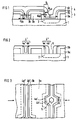
- FIG. 1 In a semiconductor substrate there is an S / D region 2 as the lower-lying conductive region to be contacted and word line 3a with an oxide encapsulation 3b on its sides and surfaces as the web-like structures defining the contact hole.
- the word lines 3a are insulated from the semiconductor substrate 1 by a gate oxide (not shown). Between adjacent encapsulated word lines 3 there are spaces which are larger over the conductive region 2 (width D 1 ) than over a part of the semiconductor substrate 1 (width D 0 ) which is not to be contacted.
- the interspace is preferably as small as possible in terms of process technology everywhere, here determined by the photo technology for producing the word lines 3a and the layer thickness of the oxide encapsulation 3b necessary for insulation.
- the widening extends over a length L 1 , which preferably corresponds approximately to the space D 1 or is somewhat smaller.
- L 1 depends, among other things, on the extent of the S / D region 2 in the word line direction.
- An insulating intermediate layer 4 is now applied over the entire surface, which in this exemplary embodiment is a double layer consisting of TEOS as the lower partial layer 4a and BPSG as the upper partial layer 4b.
- the thickness d 4 of the intermediate layer 4 (measured on the side wall of the oxide encapsulation) is chosen such that only the narrow space D 0 , but not the widened space D 1, is completely filled. It is therefore D 0/2 ⁇ d 4 ⁇ D1 / 2 and d 4 ⁇ L1 / 2 when the intermediate layer conformal deposition in about 4, this is nominally the deposited layer thickness.
- the intermediate layer 4 is the whole area etched back anisotropically until the conductive to be contacted Area 2 is at least partially exposed.
- the isolating filling remains in narrow spaces 4 ".
- Spacer 4 ' formed, which the etched contact area to enclose the S / D area 2.
- the insulating spacers 4 ' thus form the side walls of the self-aligned generated Contact hole 5, they exist in this embodiment from two adjacent partial spacers 4a ', 4b'.
- Word line 3a can also be omitted, provided that it is not (e.g. for the manufacture of so-called LDD transistors) otherwise is required because the insulation between the contact hole and Word line is also ensured by the spacers 4. In this case there is a further reduction the number of process steps, and the web-shaped Structures are represented only by the word lines 3a.
- the contact hole 5 is apparently self-aligned to the Word lines, but not to a field oxide that the S / D regions of neighboring ones in the word line direction Separates transistors from each other. The widening between The word lines must therefore be in the word line direction be sufficiently well adjusted to the S / D area, what but is generally possible without difficulty, because the contact hole is very small due to the surrounding spacers, e.g. B. smaller than the lithographically possible minimum dimension can be manufactured.
- the dimensions of the contact hole are then at least about 0.3 ⁇ in the bit line direction (i.e. perpendicular to the word lines) and 0.4 ⁇ in the word line direction.
- FIG. 3 The top view of the semiconductor substrate shows the self-aligned contact hole 5 surrounded by the BPSG spacer 4b 'and the adjacent TEOS spacer 4a'.
- the narrow spaces D 0 are completely filled with the insulating fill 4 ".
- the position of the word lines 3a is indicated by dashed lines under the oxide encapsulation 3b.
- the shape of the contact area is essentially determined by the shape of the expansion and can be approximately hexagonal, for example Filling the column, the surface is already relatively well planarized without a special planarization process (e.g. a flow process).
- the self-juiced contact hole 5 conventional, i.e. H. lithographically defined contact holes to manufacture.
- This can be the case with DRAM memories, for example be advantageous if self-aligned bit line contacts in the cell field and conventional contacts should be generated in the periphery.
- the intermediate layer 4 or BPSG layer 4b produces a photoresist mask, which in Cell field all over and in the periphery at the Make the contact holes open.
- the Interlayer is removed over the entire surface. With a Temperature step can cause the BPSG to flow will.
- This procedure creates dimensionally stable contact holes in the periphery, which are well rounded by the flow after the etching.
- a good planarization can be achieved in the periphery by using a highly doped BPSG with correspondingly good flow properties.
- the level difference between the cell array and the periphery, the z. B. arises from the storage capacitors (stacked capacitor) present only in the cell field and can complicate further processing, is reduced in the method according to the invention since the intermediate layer in the cell field is removed over the entire area.
- the periphery is thus raised relative to the cell field by d 4 (plus a possible overetch). This makes it easier to structure subsequent levels.
Landscapes
- Engineering & Computer Science (AREA)
- Manufacturing & Machinery (AREA)
- Internal Circuitry In Semiconductor Integrated Circuit Devices (AREA)
- Semiconductor Memories (AREA)
- Electrodes Of Semiconductors (AREA)
- Drying Of Semiconductors (AREA)
Description
- Figur 1 bis 2
- einen Querschnitt durch ein Halbleitersubstrat, an dem die Schritte einer Ausführungsform des Verfahrens verdeutlicht werden, wobei der Schnitt entlang der in Fig. 3 angegebenen Linie I-I verläuft, und
- Figur 3
- eine Aufsicht auf eine Ausführungsform der mit dem Verfahren hergestellten Halbleiterstruktur.
d3b= 0,2 µ
D0= 0,4 µ
D1= 1,0 µ
L1= 0,6 µ
d4a= 100 nm
d4b= 250 nm.
Claims (8)
- Herstellverfahren für ein selbstjustiertes Kontaktloch einer integrierten Halbleiterschaltung mit auf einem Halbleitersubstrat angeordneten bahnförmigen Strukturen (3), wobei das Kontaktloch (5) ein zwischen zwei bahnförmigen Strukturen befindliches, tieferliegendes leitendes Gebiet (2) mindestens teilweise freilegt,
mit folgenden Schritten:Herstellen der bahnförmigen Strukturen (3) derart, daß der Zwischenraum zwischen zwei bahnförmigen Strukturen über dem leitenden Gebiet (2) auf einer Länge L1 eine größere Breite D1 aufweist als über dem angrenzenden Halbleitersubstrat (1) mit der Breite D0,Aufbringen einer Zwischenschicht (4) mit Schichtdicke d4, wobei D1/2 > d4 ≥ D0/2 und L1/2 ≥ d4,anisotropes Ätzen der Zwischenschicht (4), bis das leitende Gebiet (2) mindestens teilweise freigelegt ist. - Verfahren nach Anspruch 1, dadurch gekennzeichnet, daß als bahnförmige Strukturen (3) isoliert auf dem Halbleitersubstrat (1) aufgebrachte Wortleitungen (3a) mit einer Oxideinkapselung (3b) und als leitendes Gebiet (2) ein im Halbleitersubstrat (1) angeordnetes dotiertes Gebiet (2) verwendet werden.
- Verfahren nach einem der Ansprüche 1 bis 2, dadurch gekennzeichnet, daß als Zwischenschicht (4) eine Doppelschicht bestehend aus einer unteren TEOS-Schicht (4a) und einer oberen hochdotierten BPSG-Schicht (4b) verwendet wird.
- Verfahren nach einem der Ansprüche 1 bis 3, dadurch gekennzeichnet, daß nach dem anisotropen Ätzen ein Temperaturschritt durchgeführt wird.
- Verfahren nach einem der Ansprüche 1 bis 4, dadurch gekennzeichnet, daß vor dem anisotropen Ätzen eine Fotolackmaske auf der Zwischenschicht (4) hergestellt wird, die ein erstes Gebiet aufweist, in welchem sie die Zwischenschicht (4) nicht bedeckt und in welchem die selbstjustierten Kontaktlöcher (5) hergestellt werden, und ein zweites Gebiet aufweist, in welchem sie die Zwischenschicht (4) im wesentlichen bedeckt und Kontakt löcher definiert, und daß das anisotrope Ätzen der Zwischenschicht unter Verwendung der Fotolackmaske durchgeführt wird, so daß gleichzeitig im ersten Gebiet selbstjustierte Kontaktlöcher und im zweiten Gebiet lithografisch definierte Kontaktlöcher hergestellt werden.
- Halbleiterstruktur mitbahnförmigen Strukturen ( 3) mit freiliegender Oberfläche auf einem Halbleitersubstrat (1),einem zwischen den bahnförmigen Strukturen ( 3) angeordneten tieferliegenden leitenden Gebiet (2), wobei der Zwischenraum zwischen zwei bahnförmigen Strukturen über einem leitenden Gebiet eine größere Breite D1 aufweist als über dem angrenzenden Halbleitersubstrat (1) mit der Breite D0,einem Kontaktloch (5) in dem vergrößerten Zwischenraum (D1), welches das leitende Gebiet (2) mindestens teilweise freilegt,einem isolierenden Spacer (4') zwischen dem Kontaktloch (5) und den Seitenwänden der bahnförmigen Strukturen (3) undeiner isolierenden Auffüllung (4'') zwischen den Seitenwänden der benachbarten bahnförmigen Strukturen (3) mit dem Abstand D0.
- Halbleiterstruktur nach Anspruch 6,
gekennzeichnet durchisoliert auf dem Halbleitersubstrat (1) aufgebrachte Wortleitungen (3a) mit einer Oxideinkapselung (3b) als bahnförmige Strukturen (3) undein im Halbleitersubstrat (1) angeordnetes dotiertes Gebiet (2) als leitendes Gebiet - Halbleiterstruktur nach Anspruch 6 oder 7,
dadurch gekennzeichnet, daßder isolierende Spacer (4') und die isolierende Auffüllung (4'') aus einer Doppelschicht, die eine TEOS-Schicht (4a) und eine BPSG-Schicht (4b) umfaßt, bestehen.
Applications Claiming Priority (2)
| Application Number | Priority Date | Filing Date | Title |
|---|---|---|---|
| DE4232621 | 1992-09-29 | ||
| DE4232621A DE4232621C1 (de) | 1992-09-29 | 1992-09-29 | Herstellverfahren für ein selbstjustiertes Kontaktloch und Halbleiterstruktur |
Publications (3)
| Publication Number | Publication Date |
|---|---|
| EP0591769A2 EP0591769A2 (de) | 1994-04-13 |
| EP0591769A3 EP0591769A3 (de) | 1994-12-14 |
| EP0591769B1 true EP0591769B1 (de) | 1999-01-20 |
Family
ID=6469129
Family Applications (1)
| Application Number | Title | Priority Date | Filing Date |
|---|---|---|---|
| EP93115286A Expired - Lifetime EP0591769B1 (de) | 1992-09-29 | 1993-09-22 | Herstellverfahren für ein selbstjustiertes Kontaktloch und Halbleiterstruktur |
Country Status (7)
| Country | Link |
|---|---|
| US (2) | US5432381A (de) |
| EP (1) | EP0591769B1 (de) |
| JP (1) | JPH06196569A (de) |
| KR (1) | KR100279014B1 (de) |
| AT (1) | ATE176085T1 (de) |
| DE (2) | DE4232621C1 (de) |
| TW (1) | TW234776B (de) |
Families Citing this family (15)
| Publication number | Priority date | Publication date | Assignee | Title |
|---|---|---|---|---|
| KR970004922B1 (ko) * | 1993-07-27 | 1997-04-08 | 삼성전자 주식회사 | 고집적 반도체 배선구조 및 그 제조방법 |
| JP2947054B2 (ja) * | 1994-03-04 | 1999-09-13 | ヤマハ株式会社 | 配線形成法 |
| JP3104534B2 (ja) * | 1994-06-27 | 2000-10-30 | ヤマハ株式会社 | 半導体装置とその製法 |
| JPH0917863A (ja) * | 1995-06-29 | 1997-01-17 | Rohm Co Ltd | 半導体装置および半導体装置の配線方法 |
| JP3277103B2 (ja) * | 1995-09-18 | 2002-04-22 | 株式会社東芝 | 半導体装置及びその製造方法 |
| JPH10321724A (ja) * | 1997-03-19 | 1998-12-04 | Fujitsu Ltd | 半導体装置およびその製造方法 |
| US6348411B1 (en) | 1998-09-03 | 2002-02-19 | Micron Technology, Inc. | Method of making a contact structure |
| US6166441A (en) * | 1998-11-12 | 2000-12-26 | Intel Corporation | Method of forming a via overlap |
| US6566759B1 (en) * | 1999-08-23 | 2003-05-20 | International Business Machines Corporation | Self-aligned contact areas for sidewall image transfer formed conductors |
| US6261924B1 (en) | 2000-01-21 | 2001-07-17 | Infineon Technologies Ag | Maskless process for self-aligned contacts |
| KR100352909B1 (ko) * | 2000-03-17 | 2002-09-16 | 삼성전자 주식회사 | 반도체소자의 자기정렬 콘택 구조체 형성방법 및 그에의해 형성된 자기정렬 콘택 구조체 |
| US6976181B2 (en) * | 2001-12-20 | 2005-12-13 | Intel Corporation | Method and apparatus for enabling a low power mode for a processor |
| KR20030087744A (ko) * | 2002-05-09 | 2003-11-15 | 삼성전자주식회사 | 집적 회로의 콘택홀 형성방법 |
| DE10342547B4 (de) * | 2003-09-12 | 2007-02-08 | Infineon Technologies Ag | Verfahren zum Herstellen einer integrierten Schaltungseinrichtung mit Durchkontaktierungselementen und Anschlusseinheiten |
| JP6212720B2 (ja) * | 2013-09-20 | 2017-10-18 | パナソニックIpマネジメント株式会社 | 半導体装置及びその製造方法 |
Family Cites Families (9)
| Publication number | Priority date | Publication date | Assignee | Title |
|---|---|---|---|---|
| US4916087A (en) * | 1988-08-31 | 1990-04-10 | Sharp Kabushiki Kaisha | Method of manufacturing a semiconductor device by filling and planarizing narrow and wide trenches |
| EP0388075B1 (de) * | 1989-03-16 | 1996-11-06 | STMicroelectronics, Inc. | Kontakte für Halbleiter-Vorrichtungen |
| JP2689703B2 (ja) * | 1989-08-03 | 1997-12-10 | 富士電機株式会社 | Mos型半導体装置 |
| JPH03201532A (ja) * | 1989-12-28 | 1991-09-03 | Casio Comput Co Ltd | 微細孔または微細溝の形成方法 |
| US5275972A (en) * | 1990-02-19 | 1994-01-04 | Matsushita Electric Industrial Co., Ltd. | Method for fabricating a semiconductor integrated circuit device including the self-aligned formation of a contact window |
| US5094900A (en) * | 1990-04-13 | 1992-03-10 | Micron Technology, Inc. | Self-aligned sloped contact |
| JPH0429318A (ja) * | 1990-05-25 | 1992-01-31 | Oki Electric Ind Co Ltd | 半導体装置の製造方法 |
| JPH04279037A (ja) * | 1991-03-07 | 1992-10-05 | Toshiba Corp | 固体撮像素子の製造方法 |
| JPH04315454A (ja) * | 1991-04-12 | 1992-11-06 | Sony Corp | 半導体装置の製造方法 |
-
1992
- 1992-09-29 DE DE4232621A patent/DE4232621C1/de not_active Expired - Fee Related
-
1993
- 1993-09-17 US US08/122,302 patent/US5432381A/en not_active Expired - Lifetime
- 1993-09-22 EP EP93115286A patent/EP0591769B1/de not_active Expired - Lifetime
- 1993-09-22 AT AT93115286T patent/ATE176085T1/de not_active IP Right Cessation
- 1993-09-22 DE DE59309324T patent/DE59309324D1/de not_active Expired - Lifetime
- 1993-09-23 TW TW082107826A patent/TW234776B/zh not_active IP Right Cessation
- 1993-09-24 JP JP5261934A patent/JPH06196569A/ja active Pending
- 1993-09-27 KR KR1019930020538A patent/KR100279014B1/ko not_active Expired - Lifetime
-
1995
- 1995-01-17 US US04/373,006 patent/US5460690A/en not_active Expired - Lifetime
Also Published As
| Publication number | Publication date |
|---|---|
| DE59309324D1 (de) | 1999-03-04 |
| TW234776B (de) | 1994-11-21 |
| US5460690A (en) | 1995-10-24 |
| JPH06196569A (ja) | 1994-07-15 |
| KR100279014B1 (ko) | 2001-02-01 |
| EP0591769A3 (de) | 1994-12-14 |
| ATE176085T1 (de) | 1999-02-15 |
| KR940007994A (ko) | 1994-04-28 |
| US5432381A (en) | 1995-07-11 |
| DE4232621C1 (de) | 1994-03-10 |
| EP0591769A2 (de) | 1994-04-13 |
Similar Documents
| Publication | Publication Date | Title |
|---|---|---|
| DE4220497B4 (de) | Halbleiterspeicherbauelement und Verfahren zu dessen Herstellung | |
| DE102004003315B4 (de) | Halbleitervorrichtung mit elektrischem Kontakt und Verfahren zur Herstellung derselben | |
| DE10107125B4 (de) | Verfahren zum Ausbilden von Kontaktlöchern in einer integrierten Schaltungsvorrichtung durch selektives Ätzen einer Isolationsschicht, um die zu einem Halbleiterbereich benachbarte selbstausrichtende Kontaktfläche zu vergrößern, und dadurch ausgebildeter Kontakt in einer integrierten Schaltungsvorrichtung | |
| DE69737783T2 (de) | Verfahren zur Herstellung eines Halbleiterspeicherbauteils | |
| DE19750918B4 (de) | Halbleitereinrichtung mit Bitleitung und Kondensatorelektrode und zugehöriges Herstellungsverfahren | |
| DE4316503C2 (de) | Verfahren zur Herstellung von Speicherzellen mit verdeckten Bitleitern | |
| DE102004021636B4 (de) | Halbleitervorrichtung mit selbstausgerichtetem vergrabenem Kontaktpaar und Verfahren zum Ausbilden desselben | |
| DE4341698B4 (de) | Halbleiterbauelement mit einem Speicherkondensator und Verfahren zu dessen Herstellung | |
| DE3785317T2 (de) | Matrix hoher Packungsdichte aus dynamischen VMOS RAM. | |
| DE3842474A1 (de) | Stapelkondensator-dram und verfahren zur herstellung derselben | |
| DE4232621C1 (de) | Herstellverfahren für ein selbstjustiertes Kontaktloch und Halbleiterstruktur | |
| DE4007582C2 (de) | Verfahren zum Herstellen von mindestens zwei Kontakten in einem Halbleiterbauelement | |
| DE3527502A1 (de) | Festwertspeicher und verfahren zur herstellung desselben | |
| EP0875937A2 (de) | DRAM-Zellenanordnung und Verfahren zu deren Herstellung | |
| DE4109299C2 (de) | Halbleiterspeichereinrichtung und Herstellungsverfahren hierfür | |
| DE4426311B4 (de) | Leiterbahnstruktur eines Halbleiterbauelementes und Verfahren zu ihrer Herstellung | |
| DE10223748B4 (de) | Verfahren zum Ausbilden einer integrierten Speicherschaltungsanordnung | |
| EP1125328B1 (de) | Verfahren zur herstellung einer dram-zellenanordnung | |
| DE19726069B4 (de) | Halbleitereinrichtung mit einer unteren und einer oberen Elektrode und zugehöriges Herstellungsverfahren | |
| DE4203565A1 (de) | Dram und verfahren zu dessen herstellung | |
| DE19709961A1 (de) | Halbleiterspeichereinrichtung und Verfahren für deren Herstellung | |
| DE10347458B4 (de) | Verfahren zur Herstellung einer Halbleitervorrichtung und nach dem Verfahren hergestellte Halbleitervorrichtung | |
| DE4441153C2 (de) | Verfahren zur Herstellung eines Kondensators einer Halbleiterspeichervorrichtung | |
| DE4411851C2 (de) | Halbleitervorrichtungen mit Grabenisolierstruktur, die einen Kanal-dotierten Bereich aufweist, und Herstellungsverfahren dafür | |
| DE4441166C2 (de) | Verfahren zur Herstellung eines Kondensators einer Halbleiterspeichervorrichtung |
Legal Events
| Date | Code | Title | Description |
|---|---|---|---|
| PUAI | Public reference made under article 153(3) epc to a published international application that has entered the european phase |
Free format text: ORIGINAL CODE: 0009012 |
|
| AK | Designated contracting states |
Kind code of ref document: A2 Designated state(s): AT DE FR GB IE IT NL |
|
| PUAL | Search report despatched |
Free format text: ORIGINAL CODE: 0009013 |
|
| AK | Designated contracting states |
Kind code of ref document: A3 Designated state(s): AT DE FR GB IE IT NL |
|
| 17P | Request for examination filed |
Effective date: 19950103 |
|
| 17Q | First examination report despatched |
Effective date: 19961022 |
|
| GRAG | Despatch of communication of intention to grant |
Free format text: ORIGINAL CODE: EPIDOS AGRA |
|
| GRAG | Despatch of communication of intention to grant |
Free format text: ORIGINAL CODE: EPIDOS AGRA |
|
| GRAH | Despatch of communication of intention to grant a patent |
Free format text: ORIGINAL CODE: EPIDOS IGRA |
|
| GRAH | Despatch of communication of intention to grant a patent |
Free format text: ORIGINAL CODE: EPIDOS IGRA |
|
| GRAA | (expected) grant |
Free format text: ORIGINAL CODE: 0009210 |
|
| AK | Designated contracting states |
Kind code of ref document: B1 Designated state(s): AT DE FR GB IE IT NL |
|
| PG25 | Lapsed in a contracting state [announced via postgrant information from national office to epo] |
Ref country code: NL Free format text: LAPSE BECAUSE OF FAILURE TO SUBMIT A TRANSLATION OF THE DESCRIPTION OR TO PAY THE FEE WITHIN THE PRESCRIBED TIME-LIMIT Effective date: 19990120 |
|
| REF | Corresponds to: |
Ref document number: 176085 Country of ref document: AT Date of ref document: 19990215 Kind code of ref document: T |
|
| REG | Reference to a national code |
Ref country code: IE Ref legal event code: FG4D Free format text: GERMAN |
|
| REF | Corresponds to: |
Ref document number: 59309324 Country of ref document: DE Date of ref document: 19990304 |
|
| ET | Fr: translation filed | ||
| ITF | It: translation for a ep patent filed | ||
| GBT | Gb: translation of ep patent filed (gb section 77(6)(a)/1977) |
Effective date: 19990323 |
|
| NLV1 | Nl: lapsed or annulled due to failure to fulfill the requirements of art. 29p and 29m of the patents act | ||
| PG25 | Lapsed in a contracting state [announced via postgrant information from national office to epo] |
Ref country code: AT Free format text: LAPSE BECAUSE OF NON-PAYMENT OF DUE FEES Effective date: 19990922 |
|
| PLBE | No opposition filed within time limit |
Free format text: ORIGINAL CODE: 0009261 |
|
| 26N | No opposition filed | ||
| REG | Reference to a national code |
Ref country code: GB Ref legal event code: IF02 |
|
| REG | Reference to a national code |
Ref country code: GB Ref legal event code: 732E Free format text: REGISTERED BETWEEN 20110804 AND 20110810 |
|
| REG | Reference to a national code |
Ref country code: FR Ref legal event code: TP Owner name: QIMONDA AG,, DE Effective date: 20120123 |
|
| PGFP | Annual fee paid to national office [announced via postgrant information from national office to epo] |
Ref country code: GB Payment date: 20120920 Year of fee payment: 20 Ref country code: IE Payment date: 20120920 Year of fee payment: 20 |
|
| PGFP | Annual fee paid to national office [announced via postgrant information from national office to epo] |
Ref country code: DE Payment date: 20121017 Year of fee payment: 20 Ref country code: FR Payment date: 20121010 Year of fee payment: 20 |
|
| PGFP | Annual fee paid to national office [announced via postgrant information from national office to epo] |
Ref country code: IT Payment date: 20120926 Year of fee payment: 20 |
|
| REG | Reference to a national code |
Ref country code: DE Ref legal event code: R071 Ref document number: 59309324 Country of ref document: DE |
|
| REG | Reference to a national code |
Ref country code: GB Ref legal event code: PE20 Expiry date: 20130921 |
|
| PG25 | Lapsed in a contracting state [announced via postgrant information from national office to epo] |
Ref country code: DE Free format text: LAPSE BECAUSE OF EXPIRATION OF PROTECTION Effective date: 20130924 |
|
| PG25 | Lapsed in a contracting state [announced via postgrant information from national office to epo] |
Ref country code: GB Free format text: LAPSE BECAUSE OF EXPIRATION OF PROTECTION Effective date: 20130921 |
|
| REG | Reference to a national code |
Ref country code: IE Ref legal event code: MK9A |
|
| PG25 | Lapsed in a contracting state [announced via postgrant information from national office to epo] |
Ref country code: IE Free format text: LAPSE BECAUSE OF EXPIRATION OF PROTECTION Effective date: 20130922 |