EP0592878A2 - Procédé et dispositif de contrôle des cartes à pointes pour tester des circuits intégrés - Google Patents
Procédé et dispositif de contrôle des cartes à pointes pour tester des circuits intégrés Download PDFInfo
- Publication number
- EP0592878A2 EP0592878A2 EP93115791A EP93115791A EP0592878A2 EP 0592878 A2 EP0592878 A2 EP 0592878A2 EP 93115791 A EP93115791 A EP 93115791A EP 93115791 A EP93115791 A EP 93115791A EP 0592878 A2 EP0592878 A2 EP 0592878A2
- Authority
- EP
- European Patent Office
- Prior art keywords
- contact
- evaluation device
- test
- needles
- needle
- Prior art date
- Legal status (The legal status is an assumption and is not a legal conclusion. Google has not performed a legal analysis and makes no representation as to the accuracy of the status listed.)
- Withdrawn
Links
- 238000012360 testing method Methods 0.000 title claims abstract description 91
- 238000000034 method Methods 0.000 title claims abstract description 45
- 239000000523 sample Substances 0.000 title 1
- 238000011156 evaluation Methods 0.000 claims abstract description 22
- 235000012431 wafers Nutrition 0.000 claims description 20
- 238000004458 analytical method Methods 0.000 claims description 16
- 230000005484 gravity Effects 0.000 claims description 5
- 230000003287 optical effect Effects 0.000 claims description 5
- 238000003384 imaging method Methods 0.000 claims description 3
- 238000001514 detection method Methods 0.000 claims 1
- 238000012937 correction Methods 0.000 abstract description 2
- 239000010410 layer Substances 0.000 description 11
- 238000004519 manufacturing process Methods 0.000 description 5
- 239000000463 material Substances 0.000 description 5
- 238000005259 measurement Methods 0.000 description 5
- 230000007547 defect Effects 0.000 description 3
- 230000000694 effects Effects 0.000 description 3
- 239000011241 protective layer Substances 0.000 description 3
- XAGFODPZIPBFFR-UHFFFAOYSA-N aluminium Chemical compound [Al] XAGFODPZIPBFFR-UHFFFAOYSA-N 0.000 description 2
- 229910052782 aluminium Inorganic materials 0.000 description 2
- QVGXLLKOCUKJST-UHFFFAOYSA-N atomic oxygen Chemical compound [O] QVGXLLKOCUKJST-UHFFFAOYSA-N 0.000 description 2
- 238000005516 engineering process Methods 0.000 description 2
- PCHJSUWPFVWCPO-UHFFFAOYSA-N gold Chemical compound [Au] PCHJSUWPFVWCPO-UHFFFAOYSA-N 0.000 description 2
- 239000010931 gold Substances 0.000 description 2
- 229910052737 gold Inorganic materials 0.000 description 2
- 229910052760 oxygen Inorganic materials 0.000 description 2
- 239000001301 oxygen Substances 0.000 description 2
- 238000011109 contamination Methods 0.000 description 1
- 230000003111 delayed effect Effects 0.000 description 1
- 230000001419 dependent effect Effects 0.000 description 1
- 230000007613 environmental effect Effects 0.000 description 1
- 238000007689 inspection Methods 0.000 description 1
- 238000009434 installation Methods 0.000 description 1
- 238000012417 linear regression Methods 0.000 description 1
- 238000012423 maintenance Methods 0.000 description 1
- 230000003647 oxidation Effects 0.000 description 1
- 238000007254 oxidation reaction Methods 0.000 description 1
- 238000002161 passivation Methods 0.000 description 1
- 238000003909 pattern recognition Methods 0.000 description 1
- 230000035515 penetration Effects 0.000 description 1
- 238000007790 scraping Methods 0.000 description 1
- 238000006748 scratching Methods 0.000 description 1
- 230000002393 scratching effect Effects 0.000 description 1
- 239000004065 semiconductor Substances 0.000 description 1
- 230000035945 sensitivity Effects 0.000 description 1
- 239000007787 solid Substances 0.000 description 1
- 238000010998 test method Methods 0.000 description 1
- 238000013519 translation Methods 0.000 description 1
- XLYOFNOQVPJJNP-UHFFFAOYSA-N water Substances O XLYOFNOQVPJJNP-UHFFFAOYSA-N 0.000 description 1
Images


Classifications
-
- G—PHYSICS
- G01—MEASURING; TESTING
- G01R—MEASURING ELECTRIC VARIABLES; MEASURING MAGNETIC VARIABLES
- G01R35/00—Testing or calibrating of apparatus covered by the other groups of this subclass
- G01R35/005—Calibrating; Standards or reference devices, e.g. voltage or resistance standards, "golden" references
-
- G—PHYSICS
- G01—MEASURING; TESTING
- G01R—MEASURING ELECTRIC VARIABLES; MEASURING MAGNETIC VARIABLES
- G01R1/00—Details of instruments or arrangements of the types included in groups G01R5/00 - G01R13/00 and G01R31/00
- G01R1/02—General constructional details
- G01R1/06—Measuring leads; Measuring probes
- G01R1/067—Measuring probes
- G01R1/073—Multiple probes
- G01R1/07307—Multiple probes with individual probe elements, e.g. needles, cantilever beams or bump contacts, fixed in relation to each other, e.g. bed of nails fixture or probe card
- G01R1/07314—Multiple probes with individual probe elements, e.g. needles, cantilever beams or bump contacts, fixed in relation to each other, e.g. bed of nails fixture or probe card the body of the probe being perpendicular to test object, e.g. bed of nails or probe with bump contacts on a rigid support
-
- G—PHYSICS
- G01—MEASURING; TESTING
- G01R—MEASURING ELECTRIC VARIABLES; MEASURING MAGNETIC VARIABLES
- G01R3/00—Apparatus or processes specially adapted for the manufacture or maintenance of measuring instruments, e.g. of probe tips
Definitions
- the invention relates to a method and a device for testing needle cards according to the preamble of patent claims 1 and 12 and of patent claims 8 and 17.
- each IC is electrically measured before sawing the wafer into the individual circuits in order to sort them according to the quality requirements.
- the wafer is placed in a test device in which its position is precisely defined.
- the contact areas (pads) of today's ICs usually have an area of 100 ⁇ m x 100 ⁇ m, whereby for the future with a reduction in the contact areas can be expected.
- the test device which electrically checks the IC must be brought into electrical contact with the contact surfaces via a so-called test card in order to ensure the electrical
- test cards used for this can have a large number of contact needles (currently up to 600 pieces) which are brought into contact with the contact surfaces (pads) of the ICs.
- the electrical connection of the contact needles to the test device is usually established via spring contacts (pogo pins) or conventional plugs.
- Test cards of this type are known from US Pat. No. 4,599,559 and DE-OS 41 01 920.
- the ICs are usually provided with a protective layer that protects them from environmental influences (moisture, dirt).
- This protective layer also called passivation, overlaps the edge of the contact areas (pads) by a few micrometers.
- This protective layer must not be damaged by the contact needle, otherwise moisture can penetrate the IC and disrupt or destroy its function.
- ICs with gold contact surfaces on which no oxide is formed: nevertheless, a thin layer of adsorbed molecules is present on these contact surfaces.
- adsorbed molecules can be water or oxygen molecules; however, other molecules from the ambient atmosphere, for example dirt molecules, can also be adsorbed.
- the oxide layer In order to establish a sufficient electrical connection between the contact needles and the contact surfaces, the oxide layer must be scratched with the contact needles to such an extent that there is sufficient contact.
- the contact needles are designed so that when the test card is placed on the wafer that contains the ICs, it is first placed with the tip on the contact surface and then when the surface pressure between the tip and the contact surface is increased by further lifting the wafer against the test card scrape the tip over the contact surface, partially scraping the oxide layer to establish an electrically conductive contact between the tip and the contact surface.
- the contact needles are usually angled and resiliently mounted in the front area, so that they do not touch the tip vertically on the contact surface, but are slightly angled, as a result of which the described "slipping" of the tip to produce a scratch is achieved when the wafer is lifted further.
- test cards For a more precise structure of the test cards, reference is made to the documents mentioned. It is clear that, given the small dimensions of the contact areas and the low thickness of the conductive layer of the contact areas, extreme care must be taken when producing the desired scratches in order to avoid damage to the contact areas.
- the correct contacting stroke for lifting the wafer against the test card, which on the one hand ensures reliable contact establishment between contact surfaces and Contact or test needles are guaranteed and, on the other hand, do not cause damage to the contact surfaces.
- the correct contact stroke depends on various parameters.
- the geometry of the test card or the contact needles plays a major role, since this determines the behavior of the contact needles when the surface pressure increases.
- the parameters to be mentioned here are in particular: tip diameter, needle shape, free length and angle of inclination of the needle to the contact surface. While on the one hand a large diameter of the needle tip is desired in order to have a sufficient contact area, a larger needle tip also causes greater damage to the contact areas if the surface pressure is too high.
- the sensitivity of the contact surfaces and the oxide layers also plays a major role, since the oxide layer is to be broken through, but the contact surfaces should not be damaged if possible. Due to the complex problems shown, the contact stroke has so far been determined empirically. If a suitable setting is found for a test card type, the series test is carried out up to a routine check that is carried out at predetermined intervals or when IC errors or defects are displayed frequently. With a corresponding control, a trained force, the operator, the test card and the IC are optically inspected; if all contact areas of the IC have even scratch marks, it is ensured that the contact pins of the test card have been in contact with the contact areas, whereby it is only unreliably recognizable whether the oxide layer has been broken or not.
- Damage to the contact surface can be seen more easily. From the optical inspection of the test card, usually only the condition of the needle tips, but not their adjustment, can be assessed well. Defects that occur more frequently are: bent needles, damaged or dirty needle tips. If the test card is not in proper condition or if the test card or the test arrangement is misaligned, the cause of the error displays caused by this is normally not recognized immediately, which leads to good ICs being treated as rejects. From the statements made it should have become clear that the previously known test methods are very labor-intensive, and the personnel must be specially trained. In addition, the known methods have a large number of sources of error which can lead to incorrect test results.
- the object of the invention is to provide a method for testing integrated circuits that works precisely, delivers reliable test results and can be largely automated. This method is said to at least reduce the failure of the test device of the so-called prober when changing the test card or when examining the test card and to avoid time-consuming tests of the test card and damage to the card due to removal and installation.
- the method enables objective statements to be made both about the position and quality of the contact needles, and about the quality of the contact surfaces and the prober used. Furthermore, an apparatus for performing the method is to be created. The object is achieved by the features of method claims 1 and 11 and device claims 6 and 16. According to the invention, a method is created in which the position and quality of the contact needles are analyzed by means of the scratches of the contact needles on a wafer by means of a pattern recognition camera and an evaluation device.
- Wafers can Finished ICs are used, so-called structured wafers, and the imprints (AI) or scratches of the contact needles on the contact areas are analyzed, or so-called unstructured, to a certain extent, "unfinished" wafers are used which have no contact areas at all, since these too have the analysis necessary Scratches occur.
- This analysis is advantageously carried out by a computer, so that the entire method can be carried out fully automatically. If, for example, the computer detects the absence of a scratch or a scratch is detected that indicates a split needle tip, the operator is given a corresponding error message after the analysis has been carried out.
- the analysis of the scratches can also be used to adjust the test device.
- the plane of the needle tips is not aligned parallel to the plane of the contact areas, stronger scratches appear on one side of the contact areas than on the opposite side.
- the location of the scratches on the contact surfaces can also be corrected after an analysis in order to obtain the scratches exactly at a specific point on the contact surface in test operation.
- the test device with the test card can be continuously and largely automatically monitored with the method according to the invention, so that any misalignments of the contact needles or damage to the test card or a misalignment of the test device can be detected immediately without the actual test process of the ICs having to be interrupted. It is not necessary to dismantle parts of the test facility or the test card.
- the method according to the invention allows extensive conclusions on the quality of the contact surfaces and the quality of the contact needles. The method can be carried out during the test operation, since it only has to be ensured that the camera intended for examining the scratches can see the scratch marks of the test needles.
- the image of the scratches can then be automatically analyzed by the computer while the test process continues, and if the scratches deviate from the target image, an alarm signal can be given or the test sequence can be stopped automatically.
- the computer can also automatically analyze the scratches.
- the scope, area, center of gravity, length, width, the beginning and the end of a scratch mark can be measured and the gray value distribution of the pinprints recorded to analyze the scratch marks.
- a differentiated gray value distribution results from so-called vibrating marks in the impression, which show cracks in the needle when it is attached and are caused by mechanical vibration or inhomogeneities of the pad material.
- These measurements can also be evaluated to adjust the test card relative to the contact areas. Since the coordinates of the contact areas are known, they can be compared with the coordinates of the scratches.
- This comparison shows, for example, that the position of the test card must be changed by means of translation and rotation in order to obtain the scratches at the desired locations on the contact surfaces.
- This correction can be carried out mathematically by converting the location-dependent data into distances from the centers of the contact areas and by making the sum of the distance squares to a minimum by means of linear regression, which results in the optimal positioning of the test card in relation to the contact areas.
- the scope of the scratches, their area and center of gravity allow conclusions to be drawn about the quality of the needle tips.
- test card does not have to be removed from the prober for the test, since the test card is checked on the basis of the scratches produced on the wafer by it. This not only saves adjustment work when the card is reinserted, it also reduces the prober's downtime. Furthermore, the test card is spared, since an additional deflection of the contact needles is not only necessary to check them, and the test card is easily damaged during assembly and disassembly. If incorrect adjustments are recognized, the test card or individual contact needles can be readjusted in the prober.
- the described method makes it possible to carry out the tests on the prober at very high temperatures - hot measurements up to 500 ° C - and to analyze the behavior of the test card and the scratches generated at these high temperatures using the scratch analysis.
- the described analysis can be used to exactly calculate the distance by which the test card has to be moved or rotated. However, it can also be established that only one or more individual contact needles are misaligned, it being possible to use the described method to calculate the amount and the direction (x, y, z) that need to be readjusted. In certain cases it can also be determined that an exchange of individual contact needles is necessary.
- the work tables used to analyze the scratches have only a certain precision with regard to the adjustment paths, which is often not sufficient for exact positioning with one control process.
- An exact measurement of any structure is therefore only possible after a calibration of the work table, by means of which the non-linearity of the drive, the wobble movement transverse to the guide and the angular errors of the guides with respect to one another are compensated. It is advantageous not to compensate at the location of the cause, which is not possible, for example, with the guides, but at the location of the effect, which means that the errors or deviations of the system are taken into account in the evaluation. According to the invention, therefore, a calibration method and a device for carrying it out are created, which make it possible to position the work table or the positioning device exactly with one control process.
- a calibration sample is placed on the work table, which contains a certain pattern and index markings.
- the pattern consists, for example, of parallel groups of lines which have a specific distance of, for example, 10 ⁇ m. If this pattern is moved under the camera field of view using the movable work table, the actual travel path can be changed be compared with the entered travel distance, and thus a calibration of the work table can be carried out.
- the computer that evaluates the camera image can always determine at which position the work table is located.
- the system can also detect that the calibration pattern has been reversed. In order to achieve a very high positioning accuracy, the entire optical system must be calibrated.
- FIG 1 shows the schematic structure of an analysis station for carrying out the method according to the invention.
- Fig. 2 shows scratch marks produced by contact needles.
- 3 shows a calibration pattern for the calibration of the test device.
- Figure 1 shows schematically the structure of an analysis station for testing test cards.
- the wafer 1 in a conventional prober, as shown, for example, in the trade journal "Solid State Technology, edition 1/91, page 16 or the trade magazine” Electronics Production and Testing Technology, edition 5/92, page 77 ", with a test card has been brought into contact and has corresponding scratch marks, the wafer 1 is positioned on a work table 2 which can be moved in the X and Y directions and a camera 6 is provided above the wafer which can see the scratch marks on the wafer Computer control, which is carried out via the evaluation device in this case, a personal computer 7, the work table 2 is moved so that the camera 6 can detect a desired position for a scratch, the camera 6 detects the actual scratch marks for optical measurement, the coordinates of which are from the computer 7 can be evaluated.
- the entire wafer 1 can be scanned by a corresponding control of the work table 2 by the computer 7; however, the work table can also be controlled manually by the operator using a joy stick 3.
- the scratch marks could also be analyzed "on-line" on the prober through the test card, for example by the camera being able to see the wafer through a window in the test card.
- Such an "on-line” method has the disadvantage that the test operation on the prober is delayed, which in most cases is not economically sensible in view of the high procurement costs of the prober and the tester required in the amount of several million DM.
- the separate test card analysis station has the advantage of being independent of the ongoing trial operation.
- the test card analysis station can be used in test card production and maintenance for constant logging of test cards by both the manufacturer and the user.
- the change in special measured values eg tip diameter
- FIG. 2 shows a calibration pattern 8 with the help of which the work table 2 is calibrated. Furthermore, the entire optical system is calibrated with the calibration pattern 8; particular attention is paid to the image scale, distortion and orthogonality.
- the calibration pattern 8 is provided with a grid that contains both parallel lines in the X and Y directions. The lines have an exact distance of 10 ⁇ m and a length of 50 ⁇ m, so that the travel path from the work table is easy can be precisely measured and calibrated; The imaging scale of the system can also be calibrated using the precisely defined line spacing. Distortion and orthogonality can be assessed via the parallelism of the lines.
- the grid has asymmetrical markings 9 which indicate the position of the field in a 100 x 100 mm calibration field within a field of 1 x 1 mm.
- the evaluation device 7 is able to detect that the calibration pattern 8 has been twisted or reversed.
- the camera used in this exemplary embodiment has a field of view of 300 ⁇ m ⁇ 300 ⁇ m, whereas the work table has a travel path of 100 mm ⁇ 100 mm.
- the index marks 10 offset from the line pattern and the asymmetrical markings 9 the evaluation device 7 can always determine the position of the work table 2 without having to assume an end point.
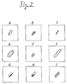
- Figure 3 shows an example of some characteristic scratch marks produced by contact needles.
- Fig. A shows a good needle mark or scratch mark, which indicates a defect-free contacting device and a good adjustment of the test card.
- the contact needles When the contact needles are placed on the surface, an ever deeper and wider scratch is created with increasing surface pressure during the scratching process. Towards the end of the scratch, the contact needle floats on the collapsed oxide skin, as a result of which the scratch trace tapers towards the end. An additional tapering of the beginning and end of the scratch is caused by the needle tip, which is usually circular in cross section.
- Picture B shows an impression consisting of two ellipses lying next to each other. This impression is generated by a split contact needle.
- a split contact needle can still make satisfactory electrical contact with the contact surfaces; Damage to the contact surfaces from the broken needle tip can hardly be avoided.
- Picture C shows the scratch mark of a needle tip that is too thin.
- This can be a contact needle that was manufactured outside the tolerance; however, it is also possible that part of the needle tip has broken off. The effects largely correspond to those of a split needle tip.
- image D shows a needle tip that is too thick. Manufacturing defects or tip contamination are possible causes. The thicker the needle tip, the lower the surface pressure generated on the contact surface for a given contacting stroke. As the thickness of the tip increases, it is therefore increasingly unlikely that the tip will penetrate the insulating oxide layer of the contact surface to a sufficient extent.
- Figure E shows a scratch that is too short
- Figure F shows a scratch that is too long.
- the length of the scratch essentially depends on the contacting stroke against the test card 3. If all needle prints show scratches that are too long, the contacting stroke is too great. And accordingly too small if the scratches are too short. However, if the pinprints of the contact needles on one side have scratches that are too long and the pinprints of the contact needles on the opposite side have scratches that are too short, the plane of the needle tips is not parallel to the plane of the contact surface. The reason for this can be a misaligned tilted test card or a test card that does not have the necessary planarity and is discarded. The test card can be distorted naturally lead to arbitrary arrangements of scratches that are too long and too short.
- Picture G shows the pinprint of a damaged tip of a contact pin.
- the broken-off area of the needle tip hardly causes any scratch marks, whereas the remaining sharp-edged part of the tip leaves strong marks on the contact surface and damages it.
- a contact needle can also have a too sharp-edged tip due to faulty manufacture, which causes damage to the contact area by digging the tip in the material of the contact area.
- a corresponding needle print is shown in picture H.
- Figure I shows a needle print of a contact needle that does not harmonize with the material of the contact surface.
- the needle digs into the material of the contact area and then slides a little over the oxide layer of the contact area, in order to then dig in again.
- the reason for this is an inadequate coordination of the contact needle and contact surface.
- a surface pressure occurs between the contact needle and the contact surface, which on the one hand prevents the needle from sliding over the surface of the contact surface and on which ensures an even penetration of the oxide layer and on the other hand allows the needle tip to be moved in such a way that it does not scratch and deep so that there is damage to the contact surfaces.
- the friction behavior essentially depends on the material of the needle tip and the contact surfaces as well as on the geometry of the needle tip and the surface structure of the contact surface.
- the images of the needle prints of the evaluation device 7 are transmitted via the camera 6, which compares them with stored typical needle prints. If, for example, a needle print is recognized that indicates a split needle tip, the analysis is carried out given the operator appropriate information.
- the result of the measurement can be output with respect to all measured parameters of the scratches (circumference, area, length, width, center of gravity, gray value distribution, beginning and end of the scratch) as mean value, standard deviation, maximum value, minimum value (x, ⁇ , x max , x min ).
- All the scratches whose measured values lie outside a predetermined tolerance range can be output, together with the measured values of the corresponding parameters and the numbers of the contact needles that produced the scratches.
- the evaluation of the grayscale distribution of different analysis devices can be adapted to one another in order to obtain a uniform evaluation scale.
Landscapes
- Physics & Mathematics (AREA)
- General Physics & Mathematics (AREA)
- Testing Or Measuring Of Semiconductors Or The Like (AREA)
Applications Claiming Priority (2)
| Application Number | Priority Date | Filing Date | Title |
|---|---|---|---|
| DE19924234856 DE4234856A1 (de) | 1992-10-15 | 1992-10-15 | Verfahren und Vorrichtung zur Prüfung von Nadelkarten für die Prüfung von integrierten Schaltkreisen |
| DE4234856 | 1992-10-15 |
Publications (2)
| Publication Number | Publication Date |
|---|---|
| EP0592878A2 true EP0592878A2 (fr) | 1994-04-20 |
| EP0592878A3 EP0592878A3 (fr) | 1995-02-01 |
Family
ID=6470584
Family Applications (1)
| Application Number | Title | Priority Date | Filing Date |
|---|---|---|---|
| EP93115791A Withdrawn EP0592878A3 (fr) | 1992-10-15 | 1993-09-30 | Procédé et dispositif de contrÔle des cartes à pointes pour tester des circuits intégrés. |
Country Status (2)
| Country | Link |
|---|---|
| EP (1) | EP0592878A3 (fr) |
| DE (1) | DE4234856A1 (fr) |
Cited By (5)
| Publication number | Priority date | Publication date | Assignee | Title |
|---|---|---|---|---|
| CN102662090A (zh) * | 2012-04-24 | 2012-09-12 | 河南正泰信创新基地有限公司 | 一种位置误差自动修正方法 |
| EP2989871A1 (fr) * | 2013-04-25 | 2016-03-02 | Finetech GmbH & Co. KG | Dispositif de placement et procédé de placement permettant d'orienter dans la bonne position un substrat et/ou de l'équiper d'un composant |
| CN108663648A (zh) * | 2017-03-27 | 2018-10-16 | 富泰华工业(深圳)有限公司 | 调校探针位置的测试板及测试方法 |
| CN114384393A (zh) * | 2020-10-22 | 2022-04-22 | 牧德科技股份有限公司 | 探针偏移的校正方法 |
| CN115598577A (zh) * | 2022-09-26 | 2023-01-13 | 国营芜湖机械厂(Cn) | 一种飞针偏差测试装置、方法及飞针测试机 |
Families Citing this family (2)
| Publication number | Priority date | Publication date | Assignee | Title |
|---|---|---|---|---|
| DE19839999C1 (de) * | 1998-09-02 | 2000-05-04 | Siemens Ag | Verfahren und Vorrichtung zum Kalibrieren eines Verfahrwegs und/oder einer Winkellage einer Haltevorrichtung in einer Einrichtung zur Herstellung von elektrischen Baugruppen sowie Kalibriersubstrat |
| CN117907793B (zh) * | 2023-11-14 | 2024-07-05 | 江苏金一辰电子科技有限公司 | 一种充电桩控制主板加工用主板测试装置 |
Family Cites Families (4)
| Publication number | Priority date | Publication date | Assignee | Title |
|---|---|---|---|---|
| JPH01282829A (ja) * | 1988-05-10 | 1989-11-14 | Canon Inc | ウエハプローバ |
| JPH0336746A (ja) * | 1989-07-04 | 1991-02-18 | Seiko Epson Corp | ウェハープローバー |
| JP2875620B2 (ja) * | 1990-09-20 | 1999-03-31 | 富士通株式会社 | ウェーハ・スケール・メモリおよびその製造方法 |
| JPH0536765A (ja) * | 1991-07-31 | 1993-02-12 | Nec Corp | プローバ |
-
1992
- 1992-10-15 DE DE19924234856 patent/DE4234856A1/de not_active Withdrawn
-
1993
- 1993-09-30 EP EP93115791A patent/EP0592878A3/fr not_active Withdrawn
Cited By (6)
| Publication number | Priority date | Publication date | Assignee | Title |
|---|---|---|---|---|
| CN102662090A (zh) * | 2012-04-24 | 2012-09-12 | 河南正泰信创新基地有限公司 | 一种位置误差自动修正方法 |
| CN102662090B (zh) * | 2012-04-24 | 2015-08-05 | 河南正泰信创新基地有限公司 | 一种位置误差自动修正方法 |
| EP2989871A1 (fr) * | 2013-04-25 | 2016-03-02 | Finetech GmbH & Co. KG | Dispositif de placement et procédé de placement permettant d'orienter dans la bonne position un substrat et/ou de l'équiper d'un composant |
| CN108663648A (zh) * | 2017-03-27 | 2018-10-16 | 富泰华工业(深圳)有限公司 | 调校探针位置的测试板及测试方法 |
| CN114384393A (zh) * | 2020-10-22 | 2022-04-22 | 牧德科技股份有限公司 | 探针偏移的校正方法 |
| CN115598577A (zh) * | 2022-09-26 | 2023-01-13 | 国营芜湖机械厂(Cn) | 一种飞针偏差测试装置、方法及飞针测试机 |
Also Published As
| Publication number | Publication date |
|---|---|
| EP0592878A3 (fr) | 1995-02-01 |
| DE4234856A1 (de) | 1994-06-01 |
Similar Documents
| Publication | Publication Date | Title |
|---|---|---|
| DE20004439U1 (de) | Sondenkartenuntersuchungssystem zur Bestimmung der Relativpositionen von Sondenspitzen | |
| DE19515154A1 (de) | Tastkopf-Meßhantiergerät, Verfahren zum Prüfen integrierter Schaltungen und integrierter Schaltungsbaustein | |
| DE60017016T2 (de) | Datenoptimierungsverfahren für Sondenkartenanalyse und Riebmarkanalyse | |
| DE10043726C2 (de) | Verfahren zum Prüfen von Leiterplatten mit einem Paralleltester und eine Vorrichtung zum Ausführen des Verfahrens | |
| DE10039928B4 (de) | Vorrichtung zum automatisierten Testen, Kalibrieren und Charakterisieren von Testadaptern | |
| EP1315975B1 (fr) | Procede et dispositif pour tester des cartes de circuits imprimes au moyen d'un testeur en parallele | |
| DE102021114358B4 (de) | Verfahren zum ausgleichen eines abstands zwischen einer probenadelspitze und einem prüfobjekt nach temperaturänderungen | |
| EP0592878A2 (fr) | Procédé et dispositif de contrôle des cartes à pointes pour tester des circuits intégrés | |
| DE112005002030T5 (de) | Vorrichtung und Verfahren zum Prüfen auf Fehler auf der Oberfläche von Werkstücken | |
| DE1918898U (de) | Zusatzgeraet fuer eine vorrichtung zum messen der oberflachenrauhigkeit. | |
| DE69707624T2 (de) | Apparat zur Inspektion von Leiterplatten | |
| DE102024121480A1 (de) | Verfahren zur Bestimmung von Sondierungsparametern für ein Sondensystem zur Prüfung einer Vorrichtung unter Test, Sondensystem und Verfahren zum Betrieb desselben, nicht-transitorische Computer-lesbare Speichermedien, Verfahren zur Prüfung einer unverpackten Halbleitervorrichtung, geprüfte Halbleitervorrichtung und Verfahren zur Herstellung derselben, und Verfahren zur Erzeugung eines virtuellen Markierungsbildes | |
| DE10355681A1 (de) | Direkte Justierung in Maskalignern | |
| DE19909298B4 (de) | Verfahren zur Kontrolle von Haltevorrichtungen für Bauelemente in Bestückautomaten | |
| DE19847146A1 (de) | Testadapter | |
| DE102012104017A1 (de) | Messeinrichtung und Verfahren zur Messung von Kugeln | |
| DE102022101274A1 (de) | Verfahren und Messanordnung zur Bestimmung der Eigenschaften einer Laserschmelzschneidvorrichtung | |
| DE4127116A1 (de) | Einrichtung zur messung mechanischer werkstoffkennwerte und zur beobachtung und auswertung von risssystemen eines bauteils | |
| DE102020108407A1 (de) | Kalibriernormal zur Geometrieeinmessung eines taktil oder/und optisch arbeitenden Messsystems, Verfahren zur Kalibrierung sowie Koordinatenmessgerät | |
| EP4325166B1 (fr) | Dispositif d'inspection optique | |
| EP4300034B1 (fr) | Procédé et système de détection des propriétés d'une section de surface sur un aéronef | |
| WO2026012529A1 (fr) | Capteur de rugosité hybride | |
| DE4438316A1 (de) | System und Verfahren zum Prüfen der korrekten Position einer Kontaktinseln und Leiterbahnen aufweisenden Leiterplatte in einer Prüfvorrichtung | |
| DD203966A1 (de) | Oberflaechenpruefgeraet, insbesondere fuer grosse messobjekte | |
| DE112023005034T5 (de) | Wirbelstromfehlerdetektionsvorrichtung und wirbelstromfehlerdetektionsverfahren |
Legal Events
| Date | Code | Title | Description |
|---|---|---|---|
| PUAI | Public reference made under article 153(3) epc to a published international application that has entered the european phase |
Free format text: ORIGINAL CODE: 0009012 |
|
| AK | Designated contracting states |
Kind code of ref document: A2 Designated state(s): AT BE CH DE FR GB LI NL SE |
|
| PUAL | Search report despatched |
Free format text: ORIGINAL CODE: 0009013 |
|
| AK | Designated contracting states |
Kind code of ref document: A3 Designated state(s): AT BE CH DE FR GB LI NL SE |
|
| STAA | Information on the status of an ep patent application or granted ep patent |
Free format text: STATUS: THE APPLICATION IS DEEMED TO BE WITHDRAWN |
|
| 18D | Application deemed to be withdrawn |
Effective date: 19950802 |