EP0593258B1 - Alimentation en courant électrique - Google Patents
Alimentation en courant électrique Download PDFInfo
- Publication number
- EP0593258B1 EP0593258B1 EP93308112A EP93308112A EP0593258B1 EP 0593258 B1 EP0593258 B1 EP 0593258B1 EP 93308112 A EP93308112 A EP 93308112A EP 93308112 A EP93308112 A EP 93308112A EP 0593258 B1 EP0593258 B1 EP 0593258B1
- Authority
- EP
- European Patent Office
- Prior art keywords
- module
- modules
- power supply
- voltage
- output
- Prior art date
- Legal status (The legal status is an assumption and is not a legal conclusion. Google has not performed a legal analysis and makes no representation as to the accuracy of the status listed.)
- Expired - Lifetime
Links
Images



Classifications
-
- H—ELECTRICITY
- H02—GENERATION; CONVERSION OR DISTRIBUTION OF ELECTRIC POWER
- H02M—APPARATUS FOR CONVERSION BETWEEN AC AND AC, BETWEEN AC AND DC, OR BETWEEN DC AND DC, AND FOR USE WITH MAINS OR SIMILAR POWER SUPPLY SYSTEMS; CONVERSION OF DC OR AC INPUT POWER INTO SURGE OUTPUT POWER; CONTROL OR REGULATION THEREOF
- H02M1/00—Details of apparatus for conversion
- H02M1/44—Circuits or arrangements for compensating for electromagnetic interference in converters or inverters
-
- H—ELECTRICITY
- H02—GENERATION; CONVERSION OR DISTRIBUTION OF ELECTRIC POWER
- H02J—ELECTRIC POWER NETWORKS; CIRCUIT ARRANGEMENTS OR SYSTEMS FOR SUPPLYING OR DISTRIBUTING ELECTRIC POWER; SYSTEMS FOR STORING ELECTRIC ENERGY
- H02J3/00—Circuit arrangements for AC mains or AC distribution networks
- H02J3/01—Arrangements for reducing harmonics or ripples
-
- H—ELECTRICITY
- H02—GENERATION; CONVERSION OR DISTRIBUTION OF ELECTRIC POWER
- H02M—APPARATUS FOR CONVERSION BETWEEN AC AND AC, BETWEEN AC AND DC, OR BETWEEN DC AND DC, AND FOR USE WITH MAINS OR SIMILAR POWER SUPPLY SYSTEMS; CONVERSION OF DC OR AC INPUT POWER INTO SURGE OUTPUT POWER; CONTROL OR REGULATION THEREOF
- H02M1/00—Details of apparatus for conversion
- H02M1/12—Arrangements for reducing harmonics from AC input or output
-
- H—ELECTRICITY
- H02—GENERATION; CONVERSION OR DISTRIBUTION OF ELECTRIC POWER
- H02M—APPARATUS FOR CONVERSION BETWEEN AC AND AC, BETWEEN AC AND DC, OR BETWEEN DC AND DC, AND FOR USE WITH MAINS OR SIMILAR POWER SUPPLY SYSTEMS; CONVERSION OF DC OR AC INPUT POWER INTO SURGE OUTPUT POWER; CONTROL OR REGULATION THEREOF
- H02M3/00—Conversion of DC power input into DC power output
- H02M3/22—Conversion of DC power input into DC power output with intermediate conversion into AC
- H02M3/24—Conversion of DC power input into DC power output with intermediate conversion into AC by static converters
- H02M3/28—Conversion of DC power input into DC power output with intermediate conversion into AC by static converters using discharge tubes with control electrode or semiconductor devices with control electrode to produce the intermediate AC
-
- Y—GENERAL TAGGING OF NEW TECHNOLOGICAL DEVELOPMENTS; GENERAL TAGGING OF CROSS-SECTIONAL TECHNOLOGIES SPANNING OVER SEVERAL SECTIONS OF THE IPC; TECHNICAL SUBJECTS COVERED BY FORMER USPC CROSS-REFERENCE ART COLLECTIONS [XRACs] AND DIGESTS
- Y02—TECHNOLOGIES OR APPLICATIONS FOR MITIGATION OR ADAPTATION AGAINST CLIMATE CHANGE
- Y02E—REDUCTION OF GREENHOUSE GAS [GHG] EMISSIONS, RELATED TO ENERGY GENERATION, TRANSMISSION OR DISTRIBUTION
- Y02E40/00—Technologies for an efficient electrical power generation, transmission or distribution
- Y02E40/40—Arrangements for reducing harmonics
Definitions
- the present invention relates to Power Supply in which a preset D.C.output voltage can be obtained from A.C.input voltage.
- Power Supply of such kind as Switching Power Supply is so structured that after obtaining D.C.input voltage by rectifying and smoothing A.C.power source supplied across a filter circuit, said D.C.input voltage is supplied to an inverter in order to optionally output stabilized D.C.voltage.
- power factor and harmonic correction circuit comprising boost-chopper type converter has come to be integrated into the Power Supply, to achieve better efficiency in energy consumption, and improve the power factor for the correction of electricity distortion and voltage drop of transmission voltage.
- US-A-4652769 discloses a multisource power supply.
- a power supply constructed by combining a plurality of modules, comprising:
- each main part constituting the power supply can be divided into an independent module, and thus each module can be optionally combined to provide a desirable power supply in accordance with various specifications thereof.
- a back-up power supply module may be provided for supplying DC input voltage to the power converter module or modules in case of abnormal stopping of the supply of said DC input voltage.
- a power supply constructed by combining a plurality of modules, the supply comprising:
- FIG.1 is a circuit diagram showing a first embodiment of a Power Supply of the present invention.
- FIG.2 is a general front view showing a first embodiment of a Power Supply of the present invention.
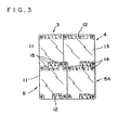
- FIG.3 is another general front view showing a first embodiment of a Power Supply of the present invention.
- FIG.4 is a circuit diagram showing a second embodiment of a Power Supply of the present invention.
- FIGS.1 to 3 show a first embodiment of the invention.
- reference numeral 1 designates A.C.power source
- 2 and 2A designate fuses respectively, in which A.C.input voltage Vin1 from A.C.power source 1 is applied to each input terminal of noise filter module 3 across said fuses 2,2A.
- Said noise filter module 3 integrates conventional noise filter circuit therein to suppress or cut-off the noise entering the line of A.C.input voltage Vin1. From the output terminals OUT of the noise filter module 3 is output D.C.input voltage Vin1, from which are eliminated the noise within a preset frequency band.
- Reference numerals 4,4A designate power factor and harmonic correction modules serving asan A.C.front end of power converter modules or D.C./D.C.converters 5,5A,5B described hereinafter.
- Said power factor and harmonic correction modules 4,4A are provided with rectifier circuit and boost-chopper type converter and the like therewithin respectively, which can bring the current and voltage waveforms of A.C.input voltage Vin1 applied to the input terminals AC close enough to each other, and correct the harmonic current from the A.C.input voltage Vin1 in order to output D.C.input voltage Vin2 from output terminals +V,-V.
- a plurality of power factor and harmonic correction modules 4,4A for various input or output voltages and output powers are provided in accordance with said A.C.input voltage Vin1 or the output power of D.C/D.C.converters 5,5A, whereby said power factor and harmonic correction modules are optionally used in a single or parallel connection thereof.
- said each power factor and harmonic correction modules 4,4A detects D.C.input voltage Vin2 so that detection signals can be supplied from detection terminals ENB when the voltage level reaches predetermined value thereof.
- Each reference numeral 5,5A,5B is provided for D.C.back end, which is D.C./D.C.converter module having a plurality of kinds for various input or output voltages and output powers.
- D.C./D.C.converter module having a plurality of kinds for various input or output voltages and output powers.
- To each input terminal +Vin,-Vin of said D.C./D.C. converters 5,5A.5B is supplied said D.C.input voltage Vin2 respectively, in which D.C.input voltage Vin2 is inverted into D.C.output voltage Vout by inverter module (not shown) integrated threrewith, and then said D.C.output voltage Vout is supplied to common load 6 across output terminals +Vout,-Vout.
- Each D.C./D.C.converter 5,5A,5B is further provided with a control terminal CNT for remote on/off control of said D.C.output voltage Vout.
- a control terminal CNT for remote on/off control of said D.C.output voltage Vout.
- said inverter will be forced to stop, so that the supply of D.C.output voltage Vout to load 6 can be shut down.
- said inverter will be controlled so that stabilized D.C.output voltage Vout can be supplied.
- reference numeral 7 is an optional unit for Power Supply, designating a back-up power supply module connected in parallel with said power factor and harmonic correction modules 4,4A.
- Said back-up power supply module 7 allows D.C.input voltage Vin2 to be supplied from output terminals +V,-V to each input terminal of each D.C./D.C.converter module 5,5A,5B when the supply of D.C.input voltage Vin2 is stopped because of some abnormal operation .
- Reference numeral 8 designates a power supply monitoring module for simultaneously observing both the input and output sides of Power Supply, which comprises a detection terminal AC1 connected to the line of A.C.input voltage Vin1 for detecting A.C.input voltage, another detection terminal DC1 connected to the line of D.C.input voltage Vin2 for detecting D.C.input, another detection terminal ENB connected to the detection terminals ENB of said power factor and harmonic correction modules 4,4A for suppressing secondary rush current, and eight detection terminals DCO1 to DCO8 connected to the line of D.C.output voltage Vout of each D.C./D.C.converter module 5,5A,5B.
- control terminals CNT of D.C./D.C.converter modules 5,5A,5B from which are supplied control signals which can perform on/off control of discrete D.C./D.C.converter modules 5,5A,5B.
- control module 9 integrating a micro computer which comprises CPU, P-ROM, input/output interface, and the like, and said converter modules are controlled in a preset condition in accordance with programs pre-written on said control module 9, in which are further provided additional functions such as display function for indicating the channel of D.C./D.C.converters 5,5A,5B causing abnormal operation, D.C.output voltage Vout and D.C.currents variable function for each D.C./D.C.converter module 5,5A,5B.
- display function for indicating the channel of D.C./D.C.converters 5,5A,5B causing abnormal operation
- D.C.output voltage Vout D.C.currents variable function for each D.C./D.C.converter module 5,5A,5B.
- FIG.2 shows a noise filter module 3, a power factor and harmonic correction module 4, D.C./D.C.converters 5,5A,5B,5C,5D laterally lined up in sequence.
- multi-output power supply can be provided by combining power factor and harmonic correction module 4 of 1KW output power, D.C./D.C.converter 5 of 300W output power,D.C./D.C.converters 5A,5B of 150 W output power, D.C./D.C.converters 5C,5D of 75 W output power with one another.
- each module 3,4,5,5A,5B,5C,5D is formed with a one-side portion 11 having the same length and height, while each of them is formed with another side portion 12 having various lengths depending upon output voltage or the like applied thereto.
- each module 3,4,5,5A,5B,5C,5D is formed with a metal core board (not shown) on which various electronics components are to be mounted. Further, each module has a cover 13 for covering over the metal core board, a press-in nut 14 with a screw hole for mounting the same to chassis or the like, and a terminal portion 15 which enables the same to be connected externally thereof.
- FIG.3 shows an approximately square-shaped Power Supply by suitably combining a noise filter module 3, a power factor and harmonic correction module 4, D.C./D.C.converters 5,5A.
- a power factor and harmonic correction module 4 of 500W output power and D.C./D.C.converters 5,5A of 150 W output power are employed.
- back-up power supply module 7 or the like can be packaged into the same shape as each module 3,4,5,5A, whereby it can be layed out on the same plane along with other modules.
- detection signals will be supplied from detection terminal ENB to power supply monitoring module 8 when D.C.input voltage Vin2 reaches a preset voltage level.
- said power supply monitoring module 8 forces each D.C./D.C.converter module 5,5A,5B to stop operating for preset time through control terminals CNT, suppressing the secondary rush current from power factor and harmonic correction modules 4,4A.
- said power supply monitoring module 8 constantly monitors A.C.input voltage Vin1, D.C.input voltage Vin2, and D.C.output voltage Vout.
- said power supply monitoring module 8 displays the channel of faulty D.C./D.C.converters 5,5A,5B, and where necessary, each D.C./D.C.converter is forced to stop operating.
- main parts constructing a Power Supply are divided into a noise filter module 3, power factor and harmonic correction module 4, D.C./D.C.converter module 5, and back-up power supply module 7 respectively, in order to be independently modularized.
- a user can optionally and easily combine each module to design Power Supply Systems with various specifications in accordance with the objects thereof.
- each module 3,4,5,7 is formed with one-side portion 11 having the same length and height, thus there will be no stepped portion in both the lateral and vertical directions on lined-up modules 3,4,5,5A,5B,5C,5D shown in FIG.2 and square-shaped modules 3,4,5,5A shown in FIG.3.
- the present Power Supply is extremely easy to operate and use for users, and general configuration of Power Supply is free to change depending upon the housing space thereof. Furthermore,since power supply monitoring module 8 having control module 9 is connnected to the designed Power Supply, a user can promptly cope with discrete abnormal operations cased therewithin.
- FIG.4 showing a second embodiment of the present invention
- the same portions as those of forgoing embodiment is designated as common reference numerals, and their repeated detail description will be omitted.
- said power factor and harmonic correction modules 4, 4A are replaced with rectifying module 21 which rectifies and smoothes A.C.input voltage Vin1 applied to input terminals AC so that D.C.input voltage Vin2 will be output from output terminals +V,-V.
- said rectifying module 21 is formed with one-side portion having the same length and height as another module, such as that of noise filter module 3, whereby the same effect and action as described in the first embodiment can be obtained.
Landscapes
- Engineering & Computer Science (AREA)
- Power Engineering (AREA)
- Physics & Mathematics (AREA)
- Electromagnetism (AREA)
- Power Conversion In General (AREA)
- Dc-Dc Converters (AREA)
- Rectifiers (AREA)
- Direct Current Feeding And Distribution (AREA)
Claims (8)
- Alimentation construite en combinant plusieurs modules, comprenant :un module de filtre antiparasite (3) pour supprimer le bruit provenant d'une ligne de tension d'entrée alternative appliquée à des bornes d'entrée (IN) et sortant la tension vers des bornes de sortie (OUT) ;des modules de facteur de puissance et de correction harmonique (4, 4A) pour rapprocher les unes des autres les formes d'onde de courant et de tension de ladite tension d'entrée alternative qui est appliquée des bornes de sortie (OUT) dudit module de filtre antiparasite (3) aux bornes d'entrée de module (AC), lesdits modules de facteur de puissance et de correction harmonique (4, 4A) supprimant le courant harmonique provenant de la tension d'entrée alternative et sortant un courant continu régulé depuis les bornes de sortie de module (+V, -V) ;des modules de convertisseurs de courant (5, 5A, 5B) pour convertir une tension continue régulée délivrée des bornes de sortie de module (+V, -V) à des bornes d'entrée de convertisseur (+Vin, -Vin) en une tension de sortie continue préréglée (Vout) au moyen d'un inverseur intégré puis pour délivrer la tension (Vout) à une charge (6) par l'intermédiaire de bornes de sortie de convertisseur (+Vout, -Vout) ;dans laquelle plusieurs types de modules sont prévus en ce qui concerne au moins lesdits modules de facteur de puissance et de correction harmonique et lesdits modules de convertisseurs de courant, de sorte que lesdits modules de facteur de puissance et de correction harmonique peuvent être utilisés dans une connexion simple ou parallèle de ces derniers, tandis que lesdits modules de convertisseurs de courant peuvent être utilisés dans une connexion simple ou multiple de ces derniers, correspondant à la caractéristique de l'alimentation.
- Alimentation selon la revendication 1, dans laquelle plusieurs modules de convertisseurs de courant (5, 5A), ayant chacun les mêmes caractéristiques de sortie, sont combinés pour un fonctionnement parallèle.
- Alimentation selon la revendication 1, dans laquelle plusieurs modules de convertisseurs de courant (5, 5A), ayant des caractéristiques de sortie différentes, sont combinés pour un fonctionnement multisortie.
- Alimentation selon la revendication 1, dans laquelle les modules comprennent en outre un module d'alimentation de secours (7) pour délivrer une tension continue de substitution auxdits modules de convertisseurs de courant (5, 5A) en cas d'interruption anormale de la délivrance de ladite tension d'entrée continue régulée depuis lesdits modules de facteur de puissance et de correction harmonique (4, 4A).
- Alimentation selon la revendication 1 ou 4, dans laquelle chaque module a respectivement une configuration quasi-carrée ou quasi-rectangulaire, et est formé d'un de ses côtés ayant la même longueur et la même hauteur.
- Alimentation selon la revendication 4, dans laquelle lesdits modules comprennent en outre un module de surveillance d'alimentation (8) ayant un module de commande pour surveiller simultanément le côté entrée et le côté sortie de l'alimentation.
- Alimentation construite en combinant plusieurs modules, l'alimentation comprenant :un module de filtre antiparasite (3) pour supprimer le bruit provenant d'une ligne de tension d'entrée alternative appliquée à des bornes d'entrée (IN) et sortant la tension vers des bornes de sortie (OUT) ;un module de redressement (21) qui redresse et lisse ladite tension d'entrée alternative qui est appliquée des bornes de sortie (OUT) dudit module de filtre antiparasite (3) aux bornes d'entrée (AC) ;des modules de convertisseurs de courant (5, 5A, 5B) pour convertir la tension continue redressée et lissée délivrée des bornes de sortie (+V, -V) du module de redressement (21) aux bornes d'entrée de module (+Vin, -Vin) en une tension de sortie continue préréglée (Vout) au moyen d'un inverseur intégré puis à délivrer la tension (Vout) à une charge (6) par l'intermédiaire de bornes de sortie de module (+Vout, -Vout) ,dans laquelle plusieurs types de modules sont prévus en ce qui concerne au moins lesdits modules de convertisseurs de courant, de sorte que lesdits modules de convertisseurs de courant peuvent être utilisés dans une connexion simple ou multiple de ces derniers, correspondant à une caractéristique de l'alimentation.
- Alimentation selon la revendication 7, dans laquelle chaque module a respectivement une configuration quasi-carrée ou quasi-rectangulaire, et est formé d'un de ses côtés ayant la même longueur et la même hauteur.
Applications Claiming Priority (2)
| Application Number | Priority Date | Filing Date | Title |
|---|---|---|---|
| JP4273248A JPH06133550A (ja) | 1992-10-12 | 1992-10-12 | 電源装置 |
| JP273248/92 | 1992-10-12 |
Publications (3)
| Publication Number | Publication Date |
|---|---|
| EP0593258A2 EP0593258A2 (fr) | 1994-04-20 |
| EP0593258A3 EP0593258A3 (fr) | 1995-02-01 |
| EP0593258B1 true EP0593258B1 (fr) | 1998-04-01 |
Family
ID=17525192
Family Applications (1)
| Application Number | Title | Priority Date | Filing Date |
|---|---|---|---|
| EP93308112A Expired - Lifetime EP0593258B1 (fr) | 1992-10-12 | 1993-10-12 | Alimentation en courant électrique |
Country Status (7)
| Country | Link |
|---|---|
| US (1) | US5530635A (fr) |
| EP (1) | EP0593258B1 (fr) |
| JP (1) | JPH06133550A (fr) |
| KR (1) | KR100217296B1 (fr) |
| DE (1) | DE69317724T2 (fr) |
| HK (1) | HK1005353A1 (fr) |
| SG (1) | SG50676A1 (fr) |
Families Citing this family (41)
| Publication number | Priority date | Publication date | Assignee | Title |
|---|---|---|---|---|
| JPH08168259A (ja) * | 1994-12-09 | 1996-06-25 | Chiyoda:Kk | インバータ型整流装置 |
| EP0741447A3 (fr) * | 1995-05-04 | 1997-04-16 | At & T Corp | Circuit et méthode pour le contrÔle d'un convertisseur avec redresseur synchrone |
| US5751150A (en) * | 1995-08-11 | 1998-05-12 | Aerovironment | Bidirectional load and source cycler |
| US5623398A (en) * | 1995-10-30 | 1997-04-22 | The United States Of America As Represented By The Administrator Of The National Aeronautics And Space Administration | Series connected converter for control of multi-bus spacecraft power utility |
| US5631550A (en) * | 1996-04-25 | 1997-05-20 | Lockheed Martin Tactical Defense Systems | Digital control for active power factor correction |
| US5731969A (en) * | 1996-07-29 | 1998-03-24 | Small; Kenneth T. | Three-phase AC power converter with power factor correction |
| FR2755803B1 (fr) * | 1996-11-08 | 1999-02-05 | Gaia Converter | Procede de montage configurable d'un convertisseur de tension continue a partir d'elements modulaires et convertisseur ainsi obtenu |
| US7269034B2 (en) | 1997-01-24 | 2007-09-11 | Synqor, Inc. | High efficiency power converter |
| US5999417A (en) | 1997-01-24 | 1999-12-07 | Fische, Llc | High efficiency power converter |
| US5883797A (en) * | 1997-06-30 | 1999-03-16 | Power Trends, Inc. | Parallel path power supply |
| ES2273399T3 (es) * | 1997-12-29 | 2007-05-01 | Alcatel | Sistema de distribucion de energia electrica. |
| IL125328A0 (en) | 1998-07-13 | 1999-03-12 | Univ Ben Gurion | Modular apparatus for regulating the harmonics of current drawn from power lines |
| DE19841133A1 (de) * | 1998-09-09 | 2000-03-16 | Abb Daimler Benz Transp | Modul einer, vorzugsweise in einem Antrieb für ein Schienenfahrzeug enthaltenen, modular aufgebauten Schaltungsanordnung |
| US6181029B1 (en) | 1998-11-06 | 2001-01-30 | International Business Machines Corporation | Method of controlling battery back-up for multiple power supplies |
| US6731523B2 (en) * | 1999-05-12 | 2004-05-04 | Ascom Energy Systems Ag | Modularized power supply |
| US6166934A (en) * | 1999-06-30 | 2000-12-26 | General Motors Corporation | High efficiency power system with plural parallel DC/DC converters |
| US6154381A (en) * | 1999-06-30 | 2000-11-28 | General Motors Corporation | High efficiency power system with plural parallel DC/DC converters |
| US6198642B1 (en) * | 1999-10-19 | 2001-03-06 | Tracewell Power, Inc. | Compact multiple output power supply |
| JP2002135975A (ja) * | 2000-10-30 | 2002-05-10 | Furukawa Battery Co Ltd:The | 電源システム |
| KR20010068087A (ko) * | 2001-04-20 | 2001-07-13 | 홍준석 | 양방향 직류 전원 공급장치 |
| DE20110841U1 (de) * | 2001-06-30 | 2001-09-20 | Dewert Antriebs- und Systemtechnik GmbH & Co KG, 32278 Kirchlengern | Elektromotorischer Stelltrieb |
| US6975098B2 (en) * | 2002-01-31 | 2005-12-13 | Vlt, Inc. | Factorized power architecture with point of load sine amplitude converters |
| US20030197428A1 (en) * | 2002-04-05 | 2003-10-23 | Hatton Thomas E. | Power processor |
| US6781352B2 (en) | 2002-12-16 | 2004-08-24 | International Rectifer Corporation | One cycle control continuous conduction mode PFC boost converter integrated circuit with integrated power switch and boost converter |
| JP3873043B2 (ja) * | 2003-08-11 | 2007-01-24 | 株式会社日立製作所 | 無停電電源装置 |
| US6967854B2 (en) * | 2003-10-30 | 2005-11-22 | Asm Assembly Automation Ltd. | Configurable power supply system for machine components |
| US6903946B1 (en) * | 2003-11-04 | 2005-06-07 | Lockheed Martin Corporation | Paralleled power factor correcting AC-to-DC converters with improved current balance |
| US20050242750A1 (en) * | 2004-04-28 | 2005-11-03 | Chin-Wen Chou | Inverter circuit with a power factor corrector |
| US7211969B2 (en) * | 2005-03-29 | 2007-05-01 | Zippy Technology Corp. | Power driver circuit of display panel |
| US7505819B2 (en) * | 2006-02-08 | 2009-03-17 | Moore Industries International, Inc. | Redundant fieldbus system |
| JP4860429B2 (ja) * | 2006-10-26 | 2012-01-25 | Tdkラムダ株式会社 | モジュール型電源装置 |
| WO2008086329A2 (fr) * | 2007-01-08 | 2008-07-17 | Continental Automotive Systems Us, Inc. | Convertisseur cc/cc |
| US8080900B2 (en) * | 2007-07-18 | 2011-12-20 | Exaflop Llc | Direct-coupled IT load |
| US20090322301A1 (en) * | 2008-06-26 | 2009-12-31 | Enermax Technology Corporation | Control circuit for improving efficiency of lower load of power supply device and method thereof |
| JP5659575B2 (ja) * | 2010-06-22 | 2015-01-28 | 株式会社リコー | マルチフェーズ型コンバータ |
| US8564989B2 (en) * | 2010-12-22 | 2013-10-22 | Intel Corporation | Cold swap load adaptive power supply |
| JP2014011925A (ja) * | 2012-07-02 | 2014-01-20 | Omron Automotive Electronics Co Ltd | 充電装置 |
| US9032250B1 (en) | 2012-11-05 | 2015-05-12 | Google Inc. | Online testing of secondary power unit |
| US10199950B1 (en) | 2013-07-02 | 2019-02-05 | Vlt, Inc. | Power distribution architecture with series-connected bus converter |
| CN105099193A (zh) * | 2014-04-16 | 2015-11-25 | 台达电子企业管理(上海)有限公司 | 直流到直流电源装置 |
| KR20220124962A (ko) | 2021-03-04 | 2022-09-14 | 삼성전자주식회사 | 전자 장치 및 전자 장치의 전력 제어 방법 |
Family Cites Families (15)
| Publication number | Priority date | Publication date | Assignee | Title |
|---|---|---|---|---|
| US3913002A (en) * | 1974-01-02 | 1975-10-14 | Gen Electric | Power circuits for obtaining a high power factor electronically |
| US4680689A (en) * | 1984-01-23 | 1987-07-14 | Donald W. Payne | Three-phase ac to dc power converter with power factor correction |
| US4652769A (en) * | 1984-02-14 | 1987-03-24 | Ion Tech, Inc. | Module power supply |
| US4783728A (en) * | 1986-04-29 | 1988-11-08 | Modular Power Corp. | Modular power supply with PLL control |
| JPS6323564A (ja) * | 1986-07-14 | 1988-01-30 | Matsushita Electric Works Ltd | 電源装置 |
| GB8817684D0 (en) * | 1988-07-25 | 1988-09-01 | Astec Int Ltd | Power factor improvement |
| US5019717A (en) * | 1988-11-14 | 1991-05-28 | Elegant Design Solutions Inc. | Computer-controlled uninterruptable power supply |
| US5184025A (en) * | 1988-11-14 | 1993-02-02 | Elegant Design Solutions, Inc. | Computer-controlled uninterruptible power supply |
| US5019954A (en) * | 1989-06-23 | 1991-05-28 | Allied-Signal Inc. | AC/DC conversion with reduced supply waveform distortion |
| JPH03143261A (ja) * | 1989-10-27 | 1991-06-18 | Koufu Nippon Denki Kk | Dc/dcコンバータ |
| JP2706740B2 (ja) * | 1990-05-16 | 1998-01-28 | セイコーインスツルメンツ株式会社 | ボルテージレギュレータ |
| JPH04217869A (ja) * | 1990-12-20 | 1992-08-07 | Nemitsuku Ramuda Kk | 電源装置 |
| US5113337A (en) * | 1991-02-08 | 1992-05-12 | General Electric Company | High power factor power supply |
| US5224029A (en) * | 1991-08-16 | 1993-06-29 | Newman Jr Robert C | Power factor and harmonic correction circuit including ac startup circuit |
| US5404092A (en) * | 1993-09-03 | 1995-04-04 | Motorola, Inc. | High power factor AC-DC converter with reactive shunt regulation |
-
1992
- 1992-10-12 JP JP4273248A patent/JPH06133550A/ja active Pending
-
1993
- 1993-10-11 KR KR1019930021012A patent/KR100217296B1/ko not_active Expired - Fee Related
- 1993-10-12 US US08/136,171 patent/US5530635A/en not_active Expired - Lifetime
- 1993-10-12 SG SG1996008452A patent/SG50676A1/en unknown
- 1993-10-12 DE DE69317724T patent/DE69317724T2/de not_active Expired - Lifetime
- 1993-10-12 EP EP93308112A patent/EP0593258B1/fr not_active Expired - Lifetime
-
1998
- 1998-05-21 HK HK98104398A patent/HK1005353A1/en not_active IP Right Cessation
Also Published As
| Publication number | Publication date |
|---|---|
| EP0593258A3 (fr) | 1995-02-01 |
| KR100217296B1 (ko) | 1999-09-01 |
| JPH06133550A (ja) | 1994-05-13 |
| US5530635A (en) | 1996-06-25 |
| EP0593258A2 (fr) | 1994-04-20 |
| KR940010465A (ko) | 1994-05-26 |
| HK1005353A1 (en) | 1998-12-31 |
| DE69317724D1 (de) | 1998-05-07 |
| SG50676A1 (en) | 1998-07-20 |
| DE69317724T2 (de) | 1998-09-10 |
Similar Documents
| Publication | Publication Date | Title |
|---|---|---|
| US5530635A (en) | Power supply | |
| HK1005353B (en) | Power supply | |
| US6856047B2 (en) | Power source apparatus | |
| US5737202A (en) | Redundant power supply system | |
| US5751564A (en) | Dual/multiple voltage level input switching power supply | |
| US5500791A (en) | Power distribution system for generating regulated DC output voltages using a dual active bridge converter driven from an unregulated DC source | |
| EP1097505B8 (fr) | Appareil modulaire servant a reguler les harmoniques d'un courant soutire de lignes d'energie electrique | |
| KR20040008610A (ko) | 중성선 전류 제거를 위한 저감된 정격의 능동 전력 필터장치 | |
| US20100054001A1 (en) | AC/DC Converter with Power Factor Correction | |
| EP1365499B1 (fr) | Circuit d'alimentation de puissance à découpage | |
| CN110649697A (zh) | 集成dc至dc转换器 | |
| EP0661453B1 (fr) | Circuit inverseur d'entraínement pour appareil de conditionnement de l'air | |
| JPH09200974A (ja) | バックアップ用蓄電池を備えた直流電源装置 | |
| US10998759B2 (en) | Uninterruptible power supply with DC output | |
| JP3330232B2 (ja) | 交直流無停電電源装置 | |
| CN210041671U (zh) | 用于高速电主轴驱动器的隔离ac-dc电源 | |
| US7468897B2 (en) | Rectifier without active switches | |
| CN1528042B (zh) | 反用换流器 | |
| EP0932237B1 (fr) | Système de distribution d'énergie électrique | |
| KR101343953B1 (ko) | 배터리 방전기를 제거한 이중변환 무정전전원장치 | |
| US6563721B1 (en) | Power supply with multiple AC input voltages | |
| JP2004127907A (ja) | 照明装置 | |
| JP2000241477A (ja) | 被試験用直流電源装置の運転方法 | |
| US20020154525A1 (en) | Circuit for converting AC voltage into DC voltage | |
| Burns et al. | Power electronics in the minicomputer industry |
Legal Events
| Date | Code | Title | Description |
|---|---|---|---|
| PUAI | Public reference made under article 153(3) epc to a published international application that has entered the european phase |
Free format text: ORIGINAL CODE: 0009012 |
|
| AK | Designated contracting states |
Kind code of ref document: A2 Designated state(s): DE FR GB NL SE |
|
| PUAL | Search report despatched |
Free format text: ORIGINAL CODE: 0009013 |
|
| RHK1 | Main classification (correction) |
Ipc: H02M 3/00 |
|
| AK | Designated contracting states |
Kind code of ref document: A3 Designated state(s): DE FR GB NL SE |
|
| 17P | Request for examination filed |
Effective date: 19950501 |
|
| 17Q | First examination report despatched |
Effective date: 19951017 |
|
| ET | Fr: translation filed |
Free format text: CORRECTIONS |
|
| GRAG | Despatch of communication of intention to grant |
Free format text: ORIGINAL CODE: EPIDOS AGRA |
|
| GRAG | Despatch of communication of intention to grant |
Free format text: ORIGINAL CODE: EPIDOS AGRA |
|
| GRAH | Despatch of communication of intention to grant a patent |
Free format text: ORIGINAL CODE: EPIDOS IGRA |
|
| GRAH | Despatch of communication of intention to grant a patent |
Free format text: ORIGINAL CODE: EPIDOS IGRA |
|
| GRAA | (expected) grant |
Free format text: ORIGINAL CODE: 0009210 |
|
| AK | Designated contracting states |
Kind code of ref document: B1 Designated state(s): DE FR GB NL SE |
|
| REF | Corresponds to: |
Ref document number: 69317724 Country of ref document: DE Date of ref document: 19980507 |
|
| ET | Fr: translation filed | ||
| PLBE | No opposition filed within time limit |
Free format text: ORIGINAL CODE: 0009261 |
|
| 26N | No opposition filed | ||
| NLT1 | Nl: modifications of names registered in virtue of documents presented to the patent office pursuant to art. 16 a, paragraph 1 |
Owner name: DENSEI-LAMBDA K.K. |
|
| REG | Reference to a national code |
Ref country code: FR Ref legal event code: CD |
|
| REG | Reference to a national code |
Ref country code: GB Ref legal event code: IF02 |
|
| NLT1 | Nl: modifications of names registered in virtue of documents presented to the patent office pursuant to art. 16 a, paragraph 1 |
Owner name: TDK-LAMBDA CORPORATION |
|
| REG | Reference to a national code |
Ref country code: FR Ref legal event code: CD |
|
| PGFP | Annual fee paid to national office [announced via postgrant information from national office to epo] |
Ref country code: DE Payment date: 20100928 Year of fee payment: 18 |
|
| PGFP | Annual fee paid to national office [announced via postgrant information from national office to epo] |
Ref country code: GB Payment date: 20101006 Year of fee payment: 18 |
|
| PGFP | Annual fee paid to national office [announced via postgrant information from national office to epo] |
Ref country code: NL Payment date: 20111025 Year of fee payment: 19 Ref country code: FR Payment date: 20111028 Year of fee payment: 19 Ref country code: SE Payment date: 20111021 Year of fee payment: 19 |
|
| REG | Reference to a national code |
Ref country code: NL Ref legal event code: V1 Effective date: 20130501 |
|
| GBPC | Gb: european patent ceased through non-payment of renewal fee |
Effective date: 20121012 |
|
| REG | Reference to a national code |
Ref country code: FR Ref legal event code: ST Effective date: 20130628 |
|
| PG25 | Lapsed in a contracting state [announced via postgrant information from national office to epo] |
Ref country code: SE Free format text: LAPSE BECAUSE OF NON-PAYMENT OF DUE FEES Effective date: 20121013 Ref country code: GB Free format text: LAPSE BECAUSE OF NON-PAYMENT OF DUE FEES Effective date: 20121012 Ref country code: DE Free format text: LAPSE BECAUSE OF NON-PAYMENT OF DUE FEES Effective date: 20130501 |
|
| REG | Reference to a national code |
Ref country code: DE Ref legal event code: R119 Ref document number: 69317724 Country of ref document: DE Effective date: 20130501 |
|
| PG25 | Lapsed in a contracting state [announced via postgrant information from national office to epo] |
Ref country code: NL Free format text: LAPSE BECAUSE OF NON-PAYMENT OF DUE FEES Effective date: 20130501 Ref country code: FR Free format text: LAPSE BECAUSE OF NON-PAYMENT OF DUE FEES Effective date: 20121031 |