EP0593922A1 - Capteur d'images à l'état solide comportant un double H-CCD à canal composite - Google Patents
Capteur d'images à l'état solide comportant un double H-CCD à canal composite Download PDFInfo
- Publication number
- EP0593922A1 EP0593922A1 EP93115298A EP93115298A EP0593922A1 EP 0593922 A1 EP0593922 A1 EP 0593922A1 EP 93115298 A EP93115298 A EP 93115298A EP 93115298 A EP93115298 A EP 93115298A EP 0593922 A1 EP0593922 A1 EP 0593922A1
- Authority
- EP
- European Patent Office
- Prior art keywords
- charge
- horizontal
- signal charge
- transferring means
- control gate
- Prior art date
- Legal status (The legal status is an assumption and is not a legal conclusion. Google has not performed a legal analysis and makes no representation as to the accuracy of the status listed.)
- Granted
Links
Images

Classifications
-
- H—ELECTRICITY
- H10—SEMICONDUCTOR DEVICES; ELECTRIC SOLID-STATE DEVICES NOT OTHERWISE PROVIDED FOR
- H10F—INORGANIC SEMICONDUCTOR DEVICES SENSITIVE TO INFRARED RADIATION, LIGHT, ELECTROMAGNETIC RADIATION OF SHORTER WAVELENGTH OR CORPUSCULAR RADIATION
- H10F39/00—Integrated devices, or assemblies of multiple devices, comprising at least one element covered by group H10F30/00, e.g. radiation detectors comprising photodiode arrays
- H10F39/10—Integrated devices
- H10F39/12—Image sensors
- H10F39/15—Charge-coupled device [CCD] image sensors
- H10F39/153—Two-dimensional or three-dimensional array CCD image sensors
-
- H—ELECTRICITY
- H04—ELECTRIC COMMUNICATION TECHNIQUE
- H04N—PICTORIAL COMMUNICATION, e.g. TELEVISION
- H04N25/00—Circuitry of solid-state image sensors [SSIS]; Control thereof
- H04N25/70—SSIS architectures; Circuits associated therewith
- H04N25/71—Charge-coupled device [CCD] sensors; Charge-transfer registers specially adapted for CCD sensors
- H04N25/713—Transfer or readout registers; Split readout registers or multiple readout registers
Definitions
- the present invention relates generally to solid state imaging devices and, more particularly, is directed to a solid state imaging device of a so-called all pixel read out type.
- CCD charge-coupled device solid state imaging devices
- CCD charge-coupled device solid state imaging devices
- Two horizontal transfer registers for example, in order to improve a resolution.
- Signal charges of odd-numbered lines and signal charges of even-numbered lines are simultaneously transferred by the two separate horizontal transfer registers and signal charges of two lines are read out during 1H (H is a horizontal scanning period) to thereby read out full pixels.
- the channel width of the horizontal transfer register must be increased in accordance therewith.
- the amount of signal charge handled by the horizontal transfer register is proportional to the area of the horizontal transfer register per bit so that the amount of signal charges handled by the horizontal transfer register can be increased by increasing the channel length and channel width of the horizontal transfer register per bit.
- the channel length of the horizontal transfer register per bit is restricted by the dimensions of an image section so that only the channel width of the horizontal transfer register is allowed to be increased.
- intensity of electric field produced in the horizontal transfer register is decreased by the horizontal transfer clock applied to the transfer electrode.
- the intensity of electric field is decreased particularly at the central portion of the horizontal transfer register in the channel width direction.
- the assignee of the present application has previously proposed a CCD solid state imaging device of all pixel read out type in which a horizontal transfer register at the image section side is formed of transfer sections of a plurality of stages (e.g., two stages) and signal charge of the same pixel is horizontally transferred by these transfer sections individually in order to increase the amount of signal charges by the horizontal transfer registers without lowering the transfer rate in the horizontal transfer register (see Japanese laid-open patent publication No. 3-72790).
- FIG. 1 of the accompanying drawings shows a structure of the conventional CCD solid state imaging device.
- a CCD image sensor section 3 of an interline transfer type comprises a plurality of photo-sensors 1 arrayed at the unit of pixel in a two-dimensional fashion and a plurality of vertical transfer registers 2 disposed at every vertical column of these photo-sensors 1 to vertically transfer signal charges generated by the photo-sensors 1.
- a first horizontal transfer register 4 is disposed under the image section 3.
- the first horizontal transfer register 4 comprises two transfer sections 4a, 4b that simultaneously transfer a signal charge of one line in the horizontal direction in a divided fashion. These transfer sections 4a, 4b are substantially the same in channel width.
- the transfer sections 4a, 4b are spaced apart a little and arranged in parallel to each other and unitarily formed as one body in an output section.
- a sum of channel widths of the transfer sections 4a, 4b becomes the channel width of the first horizontal transfer register 4.
- the value of this channel width of the first horizontal transfer register 4 is set sufficient so that the amount of signal charges handled by the first horizontal transfer register 4 can be increased sufficiently.
- a control gate section 5 is disposed between the two transfer sections 4a, 4b. A signal charge of the same pixel is distributed to transfer sections 4a, 4b under the control of the control gate section 5.
- first horizontal transfer register 4 Under the first horizontal transfer register 4 is disposed parallelly a second horizontal transfer register 6 with a small distance from the first horizontal transfer register 4.
- the channel width of the second horizontal transfer register 6 is set to be substantially the same as that of the first horizontal transfer register 4.
- a transfer gate section 7 is disposed between the first and second horizontal transfer registers 4 and 6. Under the control of the transfer gate section 7, the signal charge of one line that was transferred from the vertical transfer registers 1 to the first horizontal transfer register 4 is further transferred to the second horizontal transfer register 6.
- the signal charges horizontally transferred by the first and second horizontal transfer registers 4, 6 are converted by output sections 81, 82 into signal voltages and then developed as outputs OUT1, OUT2, respectively.
- the first horizontal transfer register 4 is formed of the transfer sections 4a, 4b of a plurality of stages (two stages in this example) as described above, the channel widths of the respective transfer sections 4a, 4b are narrow although the channel width of the first horizontal transfer register 4 is large on the whole. Thus, intensity of transfer electric field can be prevented from being lowered, and a transfer rate with which the signal charge is transferred through the first horizontal transfer register 4 to the second horizontal transfer register 6 can be avoided from being lowered.
- the amount of signal charges handled by the first horizontal transfer register 4 can be increased without lowering the transfer rate in the first horizontal transfer register 4.
- the amounts of signal charges that the two transfer sections 4a, 4b handle per bit are determined by the channel length and channel width of one bit. Therefore, when signal charges are distributed by the two transfer sections 4a, 4b, if the amount of signal charges distributed to one transfer section exceeds the amount of signal charges that the transfer section can handle, then all signal charges of one pixel cannot be transferred completely although the amount of signal charges handled by the first horizontal transfer register 4 is increased.
- a solid state imaging device provided on a semiconductor body which comprises a plurality of photo sensing elements arranged in a matrix configuration for receiving a light therein and producing a signal charge corresponding to the amount of the received light, a plurality of vertical charge transferring devices, each vertical charge transferring device arranged at one side of a vertical line of the photo sensing elements, for receiving the signal charge from the photo sensing elements and transferring the signal charge in the vertical direction, a first horizontal charge transferring device connected to the vertical charge transferring devices for receiving the signal charge transferred from a first group of alternate vertical charge transferring devices and transferring the signal charge in the horizontal direction to a charge detecting section, a second horizontal charge transferring device connected to the vertical charge transferring devices for receiving the signal charge transferred from a second group of alternate vertical charge transferring devices which are not selected as the first group of the alternate vertical charge transferring devices and transferring the signal charge in the horizontal direction to the charge detecting section, the first horizontal charge transferring device comprising first and second horizontal shift register
- a method of operating a solid state imaging device provided on a semiconductor body having a plurality of photo sensing elements for receiving a light therein and producing a signal charge, a plurality of vertical charge transferring devices for receiving and transferring the signal charge from the photo sensing elements to first and second horizontal charge transferring devices, the first and second horizontal charge transferring devices each for receiving and transferring the signal charge from the vertical charge transferring devices to a charge detecting section.
- This method comprises the steps of receiving the signal charge from a first group of alternate vertical charge transferring devices in the first horizontal charge transferring device, accumulating the signal charge under both a first horizontal shift register and a control gate, dividing the signal charge by a potential barrier located under the control gate and distributing a part of the signal charge to the first horizontal shift register, transferring the distributed signal charge in the first horizontal shift register to the charge detecting section, shifting and distributing a remaining part of the signal charge accumulated under the control gate to the second horizontal shift register, and transferring the distributed signal charge in the second horizontal shift register to the charge detecting section.
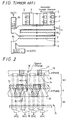
- FIG. 2 is a plan view of a CCD solid state imaging device according to an embodiment of the present invention, and illustrating only a part of the first horizontal transfer register 4 shown in FIG. 1.
- the first horizontal transfer register 4 is comprised of a plurality of stages, for example, two stages of the transfer sections 4a, 4b that are driven to horizontally transfer signal charges of one line transferred from the image section 3 (see FIG. 1) in a divided fashion.
- These transfer sections 4a, 4b are substantially the same in channel width and disposed parallelly with a small distance therebetween.
- an accumulation gate electrode (shown by a one-dot chain line) 11 and a transfer gate electrode (shown by a two-dot chain line) 12 are alternately arrayed in the horizontal transfer direction to form an electrode pair.
- the accumulation gate electrode 11 and the transfer gate electrode 12 are driven by two-phase horizontal transfer clock pulses ⁇ H1, ⁇ H2 applied to these electrode pairs.
- control gate section 5 that is used to distribute signal charges of the same pixel between the transfer sections 4a, 4b.
- the control gate section 5 has on its one portion region of the transfer section 4a side a potential barrier section 13 extended along the horizontal transfer direction.
- the potential barrier section 13 is formed by implanting impurity of conductivity type opposite to that of impurity forming a transfer channel at the position at which the potential barrier section 13 is to be formed or by implanting impurity of the same conductivity type in the region of the control gate section 5 except the position at which the potential barrier section 13 is to be formed. Further, the potential barrier section 13 can be formed by controlling a film thickness of a gate oxide film (not shown) of the control gate section 5. In FIG. 2, a hatched area 14 represents a channel stopper section.
- ⁇ VH2 is a gate pulse applied to a gate electrode 15 of the output section of the vertical transfer register 2
- ⁇ H1 is a first phase pulse of the two-phase horizontal transfer clocks.
- ⁇ HHG is a gate pulse applied to a gate electrode 16 of the control gate section 5.
- a horizontal transfer clock pulse ⁇ H2 of a second phase is not shown in FIG. 3 because the horizontal transfer clock pulse ⁇ H2 is constantly held at high level at a timing of distributing a signal charge.
- FIG. 4 is a diagram of potential at a cross section taken along the line IV - IV in FIG. 2.
- times T1 to T5 are corresponding to times T1 to T5 in FIG. 3, respectively.
- Time T1 shows the condition just before a signal charge is transferred from the vertical transfer register 2 to the first horizontal transfer register 4.
- the signal charge from the vertical transfer register 2 is transferred to the transfer section 4a and the control gate section 5.
- much signal charges are accumulated in the region of the control gate section 5 other than the potential barrier section 13 because the potential barrier section 13 is formed on the control gate section 5.
- the amount of the signal charges is determined by the area of the control gate section 5 at its region in which the potential barrier section 13 is not formed and the potential of the potential barrier section 13. This amount of signal charges becomes the amount of signal charges transferred by the transfer section 4b. At that time, the potential of the potential barrier section 13 is set to be the same as or deeper than the potential of the transfer section 4b.
- the amount of signal charges that can be accumulated in the control gate section 5 is limited, signal charges that could not be accumulated in the control gate section 5 are overflown from the potential barrier section 13 and accumulated in the region of the transfer section 4a. That is to say, the amount of signal charges transferred by the transfer section 4a in the horizontal direction becomes equal to the signal charge amount that results from subtracting the amount of signal charges horizontally transferred by the transfer section 4b from the amount of all signal charges transferred from the vertical transfer register 2.
- the clock pulse ⁇ H1 goes to high level and the potential of the transfer section 4b becomes deep so that signal charges accumulated in the control gate section 5 are transferred to the transfer section 4b.
- the gate pulse ⁇ HHG goes to low level, whereby the potential of the control gate section 5 becomes shallowest.
- the signal charges of the same pixel transferred to the first horizontal transfer register 4 from the vertical transfer register 2 are distributed between the transfer sections 4a and 4b on the basis of the amount of signal charges handled by the transfer section 4b.
- the signal charges distributed between the transfer sections 4a and 4b are returned to the signal charge of one pixel amount again after they had been transferred in the horizontal direction.
- the channels of the transfer sections 4a, 4b must be coupled together, for example, in a final stage of the first horizontal transfer register 4, i.e., place in which the first horizontal transfer register 4 need not be divided into two stages, whereby separated signal charges can be formed into a lump of signal charges again when signal charges are transferred in the horizontal direction.
- the place in which the first horizontal transfer register 4 need not be divided into two stages is, in the structure of FIG. 1, for example, a place where signal charges need not be transferred from the first horizontal transfer register 4 to the second horizontal transfer register 6, to be more concrete, a horizontal dummy bit or the like where an effective pixel signal is not transferred from the vertical transfer register 2 to the first horizontal transfer register 4.
- the gate pulse ⁇ HHG is not limited to the three-value level clock and the following variant also is possible. That is, if a speed at which the gate pulse ⁇ HHG falls is decreased adequately by some suitable means such as a delay circuit or the like, then it becomes possible to distribute signal charge.
- the present invention is applied to the solid state imaging device in which the first horizontal transfer register 4 is divided into two stages as described above, the number of stages that the first horizontal transfer register 4 is divided is not limited to two stage and may of course be three stages or more.
- signal charges need not be distributed between the transfer sections 4a, 4b in consideration of the amount of signal charges handled by the respective transfer sections 4a, 4b, signal charges can be distributed between the transfer sections 4a and 4b by making the potential of the control gate section 5 become shallow without changing the potentials of the transfer sections 4a, 4b after the signal charges from the vertical transfer register 2 had been accumulated in the whole first horizontal transfer register 4 including the control gate section 5.
- signal charges are distributed between the transfer sections 4a and 4b without considering the amount of signal charges handled by the respective transfer sections 4a, 4b, signal charges can be transferred more smoothly from the first horizontal transfer register 4 to the second horizontal transfer register 6 in the horizontal direction because potential of the control gate section 5 in the first horizontal transfer register 4 (image section 3) side is high but is low in the opposite side due to the potential barrier section 13 existing in the control gate section 5.
- the control gate section that distributes signal charges between respective transfer sections has at its one portion of region the potential barrier section formed along the horizontal transfer direction. After signal charges had been accumulated in the control gate section, the signal charges are distributed between the transfer sections by controlling a relative potential difference between the control gate section and the transfer sections. Therefore, the amount of signal charges transferred by one transfer section is determined by the area of the control gate section at its region in which the potential barrier section is not formed and the potential of the potential barrier section. Thus, by determining the amount of signal charges on the basis of the amount of signal charges handled by the transfer section, signal charges can be distributed between the respective transfer sections in consideration of the amount of signal charges that the respective transfer sections can handle.
- control gate section has on its one portion of the region near the image section side the potential barrier section formed, the potential which is high in the image section side and low in the opposite side is generated in the control gate section. Therefore, when signal charges are vertically transferred from the horizontal transfer register on the image section side to the horizontal transfer register on the opposite side, such transferring of signal charges can be carried out more smoothly.
Landscapes
- Engineering & Computer Science (AREA)
- Multimedia (AREA)
- Signal Processing (AREA)
- Solid State Image Pick-Up Elements (AREA)
- Transforming Light Signals Into Electric Signals (AREA)
- Electrophonic Musical Instruments (AREA)
Applications Claiming Priority (3)
| Application Number | Priority Date | Filing Date | Title |
|---|---|---|---|
| JP277867/92 | 1992-09-22 | ||
| JP27786792 | 1992-09-22 | ||
| JP27786792A JP3271200B2 (ja) | 1992-09-22 | 1992-09-22 | 固体撮像装置およびその駆動方法 |
Publications (2)
| Publication Number | Publication Date |
|---|---|
| EP0593922A1 true EP0593922A1 (fr) | 1994-04-27 |
| EP0593922B1 EP0593922B1 (fr) | 2000-01-19 |
Family
ID=17589393
Family Applications (1)
| Application Number | Title | Priority Date | Filing Date |
|---|---|---|---|
| EP93115298A Expired - Lifetime EP0593922B1 (fr) | 1992-09-22 | 1993-09-22 | Capteur d'images à l'état solide comportant un double H-CCD à canal composite |
Country Status (5)
| Country | Link |
|---|---|
| US (1) | US5387935A (fr) |
| EP (1) | EP0593922B1 (fr) |
| JP (1) | JP3271200B2 (fr) |
| KR (2) | KR970005989B1 (fr) |
| DE (1) | DE69327629T2 (fr) |
Cited By (4)
| Publication number | Priority date | Publication date | Assignee | Title |
|---|---|---|---|---|
| EP0705029A3 (fr) * | 1994-09-27 | 1996-06-26 | Sony Corp | Capteur d'image à l'état solide |
| EP0795909A3 (fr) * | 1996-03-14 | 1998-12-23 | Sony Corporation | Capteur d'image à l'état solide, méthode de commande et utilisation dans une caméra |
| GB2395068A (en) * | 2002-10-04 | 2004-05-12 | E2V Tech Uk Ltd | Solid state imager |
| DE19802818B4 (de) * | 1997-01-25 | 2006-03-30 | Magnachip Semiconductor, Ltd. | CCD-Festkörper-Bildaufnahmevorrichtung, Verfahren zum Abbilden eines Bereichs von Bildspannungen auf einen Standardbereich, das in der CCD-Festkörper-Bildaufnahmevorrichtung verwendet wird, sowie Verfahren zum Betreiben der CCD-Festkörper-Bildaufnahmevorrichtung |
Families Citing this family (9)
| Publication number | Priority date | Publication date | Assignee | Title |
|---|---|---|---|---|
| JP3088591B2 (ja) * | 1993-06-17 | 2000-09-18 | 松下電器産業株式会社 | 固体撮像装置および駆動方法 |
| US5786852A (en) * | 1994-06-20 | 1998-07-28 | Canon Kabushiki Kaisha | Image pick-up apparatus having an image sensing device including a photoelectric conversion part and a vertical transfer part |
| US6157408A (en) * | 1995-06-06 | 2000-12-05 | Takeharu Etoh | High-speed CCD image transfer apparatus |
| JP3492029B2 (ja) * | 1995-06-30 | 2004-02-03 | キヤノン株式会社 | 撮像装置 |
| US20020057349A1 (en) | 1996-03-06 | 2002-05-16 | Masanori Yamaguchi | Image pickup apparatus and solid state image pickup device |
| JP2000164848A (ja) * | 1998-11-27 | 2000-06-16 | Sony Corp | 固体撮像装置及びその駆動方法 |
| JP4333664B2 (ja) | 2005-11-11 | 2009-09-16 | ソニー株式会社 | 固体撮像素子及び固体撮像装置 |
| JP2007173774A (ja) * | 2005-11-22 | 2007-07-05 | Matsushita Electric Ind Co Ltd | 固体撮像装置 |
| JP4431990B2 (ja) * | 2005-12-14 | 2010-03-17 | ソニー株式会社 | 固体撮像装置 |
Citations (3)
| Publication number | Priority date | Publication date | Assignee | Title |
|---|---|---|---|---|
| US4807037A (en) * | 1987-03-06 | 1989-02-21 | Kabushiki Kaisha Toshiba | Low noise CCD image sensor having a plurality of horizontal CCD registers |
| EP0383519A2 (fr) * | 1989-02-14 | 1990-08-22 | Sony Corporation | Dispositif de prise de vue à CCD ayant une structure de lecture multicanal |
| JPH0372790A (ja) * | 1989-08-11 | 1991-03-27 | Sony Corp | 固体撮像装置 |
Family Cites Families (4)
| Publication number | Priority date | Publication date | Assignee | Title |
|---|---|---|---|---|
| FR2629229B1 (fr) * | 1988-03-23 | 1992-09-11 | Thomson Csf | Dispositif de lecture des quantites de charges electriques fournies par des photodiodes a substrat semi-conducteur |
| US5182623A (en) * | 1989-11-13 | 1993-01-26 | Texas Instruments Incorporated | Charge coupled device/charge super sweep image system and method for making |
| US5196939A (en) * | 1989-12-28 | 1993-03-23 | Loral Fairchild Corporation | Method and apparatus for transferring images from an imaging array |
| US5040071A (en) * | 1990-03-21 | 1991-08-13 | Eastman Kodak Company | Image sensor having multiple horizontal shift registers |
-
1992
- 1992-09-22 JP JP27786792A patent/JP3271200B2/ja not_active Expired - Lifetime
-
1993
- 1993-04-14 KR KR1019930006250A patent/KR970005989B1/ko not_active Expired - Fee Related
- 1993-09-17 KR KR1019930018760A patent/KR100274077B1/ko not_active Expired - Fee Related
- 1993-09-21 US US08/124,211 patent/US5387935A/en not_active Expired - Fee Related
- 1993-09-22 DE DE69327629T patent/DE69327629T2/de not_active Expired - Fee Related
- 1993-09-22 EP EP93115298A patent/EP0593922B1/fr not_active Expired - Lifetime
Patent Citations (3)
| Publication number | Priority date | Publication date | Assignee | Title |
|---|---|---|---|---|
| US4807037A (en) * | 1987-03-06 | 1989-02-21 | Kabushiki Kaisha Toshiba | Low noise CCD image sensor having a plurality of horizontal CCD registers |
| EP0383519A2 (fr) * | 1989-02-14 | 1990-08-22 | Sony Corporation | Dispositif de prise de vue à CCD ayant une structure de lecture multicanal |
| JPH0372790A (ja) * | 1989-08-11 | 1991-03-27 | Sony Corp | 固体撮像装置 |
Non-Patent Citations (1)
| Title |
|---|
| PATENT ABSTRACTS OF JAPAN vol. 15, no. 240 (E - 1079) 20 June 1991 (1991-06-20) * |
Cited By (8)
| Publication number | Priority date | Publication date | Assignee | Title |
|---|---|---|---|---|
| EP0705029A3 (fr) * | 1994-09-27 | 1996-06-26 | Sony Corp | Capteur d'image à l'état solide |
| US5812192A (en) * | 1994-09-27 | 1998-09-22 | Sony Corporation | Solid state imaging apparatus having a channel stop section for forming a transfer channel between first and second transfer sections in a horizontal transfer register |
| EP0795909A3 (fr) * | 1996-03-14 | 1998-12-23 | Sony Corporation | Capteur d'image à l'état solide, méthode de commande et utilisation dans une caméra |
| US6002146A (en) * | 1996-03-14 | 1999-12-14 | Sony Corporation | Solid-State image sensing device, method for driving thereof and camera employing the same |
| DE19802818B4 (de) * | 1997-01-25 | 2006-03-30 | Magnachip Semiconductor, Ltd. | CCD-Festkörper-Bildaufnahmevorrichtung, Verfahren zum Abbilden eines Bereichs von Bildspannungen auf einen Standardbereich, das in der CCD-Festkörper-Bildaufnahmevorrichtung verwendet wird, sowie Verfahren zum Betreiben der CCD-Festkörper-Bildaufnahmevorrichtung |
| GB2395068A (en) * | 2002-10-04 | 2004-05-12 | E2V Tech Uk Ltd | Solid state imager |
| GB2395068B (en) * | 2002-10-04 | 2006-01-04 | E2V Tech Uk Ltd | Solid state imager |
| US7173229B2 (en) | 2002-10-04 | 2007-02-06 | E2V Technologies (Uk) Limited | Solid state imager |
Also Published As
| Publication number | Publication date |
|---|---|
| KR970005989B1 (ko) | 1997-04-22 |
| KR100274077B1 (ko) | 2000-12-15 |
| US5387935A (en) | 1995-02-07 |
| JPH06105239A (ja) | 1994-04-15 |
| DE69327629D1 (de) | 2000-02-24 |
| JP3271200B2 (ja) | 2002-04-02 |
| KR940008432A (ko) | 1994-04-29 |
| KR940024663A (ko) | 1994-11-18 |
| EP0593922B1 (fr) | 2000-01-19 |
| DE69327629T2 (de) | 2000-06-29 |
Similar Documents
| Publication | Publication Date | Title |
|---|---|---|
| US4602289A (en) | Solid state image pick-up device | |
| US7430006B2 (en) | Charge transfer device and a driving method thereof and a driving method for solid-state image sensing device | |
| EP0313322B1 (fr) | Dispositif de prise d'images à semi-conducteur ayant plusieurs portions de transfert horizontal | |
| EP0593922B1 (fr) | Capteur d'images à l'état solide comportant un double H-CCD à canal composite | |
| US4518978A (en) | Solid state image sensor | |
| US5379067A (en) | CCD linear sensor and method of reading-out charges therefrom | |
| EP0513666A1 (fr) | Registre à décalage à transfert de charges | |
| US5365093A (en) | Solid-state imaging device with tapered channel regions | |
| US5317408A (en) | Horizontally aligned image pickup for CCD image sensor | |
| EP0553869B1 (fr) | Procédé de transfert de charges, dispositif à transfert de charge et capteur d'image à l'état solide l'utilisant | |
| JPH02309877A (ja) | 固体撮像装置 | |
| US5812192A (en) | Solid state imaging apparatus having a channel stop section for forming a transfer channel between first and second transfer sections in a horizontal transfer register | |
| US20070291150A1 (en) | Solid-state image pickup device having an accumulation gate for reading out, accumulating, and allocating signal charges | |
| KR100339294B1 (ko) | 고체 이미지 센싱 장치와 그 구동방법 | |
| EP0520605B1 (fr) | Détecteur d'image à l'état solide et méthode de commande attenante | |
| JPS6210469B2 (fr) | ||
| EP0519442B1 (fr) | Dispositif CCD de prise de vue | |
| JP2820019B2 (ja) | 固体撮像素子 | |
| JP3185230B2 (ja) | 固体撮像装置 | |
| JPH0666346B2 (ja) | 電荷結合素子およびその駆動方法 | |
| JPH1127476A (ja) | 固体撮像装置 | |
| JPH0693766B2 (ja) | 固体撮像装置 | |
| JPH045308B2 (fr) | ||
| JPS63234677A (ja) | 電荷結合素子の駆動方法 | |
| JPH07162754A (ja) | 固体撮像装置 |
Legal Events
| Date | Code | Title | Description |
|---|---|---|---|
| PUAI | Public reference made under article 153(3) epc to a published international application that has entered the european phase |
Free format text: ORIGINAL CODE: 0009012 |
|
| AK | Designated contracting states |
Kind code of ref document: A1 Designated state(s): DE FR GB |
|
| 17P | Request for examination filed |
Effective date: 19940927 |
|
| 17Q | First examination report despatched |
Effective date: 19970227 |
|
| GRAG | Despatch of communication of intention to grant |
Free format text: ORIGINAL CODE: EPIDOS AGRA |
|
| GRAG | Despatch of communication of intention to grant |
Free format text: ORIGINAL CODE: EPIDOS AGRA |
|
| GRAG | Despatch of communication of intention to grant |
Free format text: ORIGINAL CODE: EPIDOS AGRA |
|
| GRAH | Despatch of communication of intention to grant a patent |
Free format text: ORIGINAL CODE: EPIDOS IGRA |
|
| RTI1 | Title (correction) |
Free format text: SOLID STATE IMAGING DEVICE HAVING DUAL-H-CCD WITH A COMPOUND CHANNEL |
|
| GRAH | Despatch of communication of intention to grant a patent |
Free format text: ORIGINAL CODE: EPIDOS IGRA |
|
| GRAA | (expected) grant |
Free format text: ORIGINAL CODE: 0009210 |
|
| AK | Designated contracting states |
Kind code of ref document: B1 Designated state(s): DE FR GB |
|
| REF | Corresponds to: |
Ref document number: 69327629 Country of ref document: DE Date of ref document: 20000224 |
|
| ET | Fr: translation filed | ||
| PLBE | No opposition filed within time limit |
Free format text: ORIGINAL CODE: 0009261 |
|
| 26N | No opposition filed | ||
| REG | Reference to a national code |
Ref country code: GB Ref legal event code: IF02 |
|
| PGFP | Annual fee paid to national office [announced via postgrant information from national office to epo] |
Ref country code: FR Payment date: 20020910 Year of fee payment: 10 |
|
| PGFP | Annual fee paid to national office [announced via postgrant information from national office to epo] |
Ref country code: GB Payment date: 20020918 Year of fee payment: 10 |
|
| PGFP | Annual fee paid to national office [announced via postgrant information from national office to epo] |
Ref country code: DE Payment date: 20020925 Year of fee payment: 10 |
|
| PG25 | Lapsed in a contracting state [announced via postgrant information from national office to epo] |
Ref country code: GB Free format text: LAPSE BECAUSE OF NON-PAYMENT OF DUE FEES Effective date: 20030922 |
|
| PG25 | Lapsed in a contracting state [announced via postgrant information from national office to epo] |
Ref country code: DE Free format text: LAPSE BECAUSE OF NON-PAYMENT OF DUE FEES Effective date: 20040401 |
|
| GBPC | Gb: european patent ceased through non-payment of renewal fee |
Effective date: 20030922 |
|
| PG25 | Lapsed in a contracting state [announced via postgrant information from national office to epo] |
Ref country code: FR Free format text: LAPSE BECAUSE OF NON-PAYMENT OF DUE FEES Effective date: 20040528 |
|
| REG | Reference to a national code |
Ref country code: FR Ref legal event code: ST |