EP0594427B1 - Plaque à circuit imprimé avec des éléments électriques montés dessus - Google Patents
Plaque à circuit imprimé avec des éléments électriques montés dessus Download PDFInfo
- Publication number
- EP0594427B1 EP0594427B1 EP93308379A EP93308379A EP0594427B1 EP 0594427 B1 EP0594427 B1 EP 0594427B1 EP 93308379 A EP93308379 A EP 93308379A EP 93308379 A EP93308379 A EP 93308379A EP 0594427 B1 EP0594427 B1 EP 0594427B1
- Authority
- EP
- European Patent Office
- Prior art keywords
- electric elements
- electrolysis
- plate layer
- printed circuit
- lands
- Prior art date
- Legal status (The legal status is an assumption and is not a legal conclusion. Google has not performed a legal analysis and makes no representation as to the accuracy of the status listed.)
- Expired - Lifetime
Links
Images


Classifications
-
- H—ELECTRICITY
- H05—ELECTRIC TECHNIQUES NOT OTHERWISE PROVIDED FOR
- H05K—PRINTED CIRCUITS; CASINGS OR CONSTRUCTIONAL DETAILS OF ELECTRIC APPARATUS; MANUFACTURE OF ASSEMBLAGES OF ELECTRICAL COMPONENTS
- H05K3/00—Apparatus or processes for manufacturing printed circuits
- H05K3/22—Secondary treatment of printed circuits
- H05K3/24—Reinforcing of the conductive pattern
- H05K3/244—Finish plating of conductors, especially of copper conductors, e.g. for pads or lands
-
- H—ELECTRICITY
- H05—ELECTRIC TECHNIQUES NOT OTHERWISE PROVIDED FOR
- H05K—PRINTED CIRCUITS; CASINGS OR CONSTRUCTIONAL DETAILS OF ELECTRIC APPARATUS; MANUFACTURE OF ASSEMBLAGES OF ELECTRICAL COMPONENTS
- H05K1/00—Printed circuits
- H05K1/18—Printed circuits structurally associated with non-printed electric components
- H05K1/181—Printed circuits structurally associated with non-printed electric components associated with surface mounted components
-
- H—ELECTRICITY
- H05—ELECTRIC TECHNIQUES NOT OTHERWISE PROVIDED FOR
- H05K—PRINTED CIRCUITS; CASINGS OR CONSTRUCTIONAL DETAILS OF ELECTRIC APPARATUS; MANUFACTURE OF ASSEMBLAGES OF ELECTRICAL COMPONENTS
- H05K2201/00—Indexing scheme relating to printed circuits covered by H05K1/00
- H05K2201/10—Details of components or other objects attached to or integrated in a printed circuit board
- H05K2201/10613—Details of electrical connections of non-printed components, e.g. special leads
- H05K2201/10621—Components characterised by their electrical contacts
- H05K2201/10681—Tape Carrier Package [TCP]; Flexible sheet connector
-
- H—ELECTRICITY
- H05—ELECTRIC TECHNIQUES NOT OTHERWISE PROVIDED FOR
- H05K—PRINTED CIRCUITS; CASINGS OR CONSTRUCTIONAL DETAILS OF ELECTRIC APPARATUS; MANUFACTURE OF ASSEMBLAGES OF ELECTRICAL COMPONENTS
- H05K3/00—Apparatus or processes for manufacturing printed circuits
- H05K3/36—Assembling printed circuits with other printed circuits
- H05K3/361—Assembling flexible printed circuits with other printed circuits
-
- Y—GENERAL TAGGING OF NEW TECHNOLOGICAL DEVELOPMENTS; GENERAL TAGGING OF CROSS-SECTIONAL TECHNOLOGIES SPANNING OVER SEVERAL SECTIONS OF THE IPC; TECHNICAL SUBJECTS COVERED BY FORMER USPC CROSS-REFERENCE ART COLLECTIONS [XRACs] AND DIGESTS
- Y02—TECHNOLOGIES OR APPLICATIONS FOR MITIGATION OR ADAPTATION AGAINST CLIMATE CHANGE
- Y02P—CLIMATE CHANGE MITIGATION TECHNOLOGIES IN THE PRODUCTION OR PROCESSING OF GOODS
- Y02P70/00—Climate change mitigation technologies in the production process for final industrial or consumer products
- Y02P70/50—Manufacturing or production processes characterised by the final manufactured product
Definitions
- This invention relates to a printed circuit board mounted with electric elements thereon, and more particularly to, a printed circuit board mounted with electric elements thereon by at least two different mounting methods and surface treating methods.
- a conventional printed circuit board has lands for surface-mounted devices (SMDs), wherein the lands each comprises a predetermined pattern of copper foils, and non-electrolysis Ni-Au plates covering the copper foils.
- SMDs surface-mounted devices
- the conventional PCB has disadvantages in that only packaged devices can be mounted thereon due to the application of heat for the re-flow process, high density mounting of the SMDs can not be realized, due to the use of the FPC connector, and the thickness, volume and weight are significantly greater than is desirable.
- JP 4-051582 describes a hybrid integrated circuit device in which a semiconductor chip is die bonded to an electric-component mounting part of a flexible wiring board and a chip capacitor is soldered and mounted on a wiring part of the wiring board.
- the present invention provides a printed circuit board comprising lands for mounting electric elements on the printed circuit board, characterised in that said lands comprise at least two of:
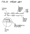
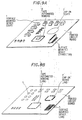
- Fig. 1A shows the conventional PCB 12, on the top surface of which various SMDs including chips 1 such as resistances and capacitors which are molded by ceramic, plastic, etc., a SOP 2 which is packaged by plastic, etc., a connector 3 for connecting internal circuits on the PCB to external circuits, and a QFP 9 are provided.
- chips 1 such as resistances and capacitors which are molded by ceramic, plastic, etc.
- SOP 2 which is packaged by plastic, etc.
- a connector 3 for connecting internal circuits on the PCB to external circuits
- QFP 9 QFP 9
- Figs. 1B and 1C show the PCB having a through-hole (only in Fig. 1C) and SMD lands 5, wherein each of the SMD lands 5 comprises a predetermined pattern of a copper foil 51 and a non-electrolysis Ni-Au plate 52 functioning as a surface-treating layer, provided that Fig. 1C does not correspond to Fig. 1B precisely, and only has illustrative purpose.
- cream solder is supplied on the SMD lands 5 on the PCB 12, and the SMDs 1, 2, 3 and 9 are positioned thereon. Then, thermal treatment is carried out by heating the PCB 12 at a predetermined temperature. Thus, the re-flow process takes place to fabricate the PCB 12 mounted with electric elements thereon.
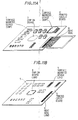
- Fig. 2A shows a PCB mounted with electric elements thereon in the first preferred embodiment according to the invention, wherein like parts are indicated by like reference numerals as used in Fig. 1A.
- a TAB for mounting a tape carrier package 4 which is a semiconductor device other than IC and LSI is provided on the PCB 12 in addition to the aforementioned SMDs 1, 2 and 3.
- Figs. 2B and 2C show the PCB 12 having a through-hole (only in Fig. 2C), SMD lands 5 and a TAB land 6, wherein the TAB land 6 comprises a predetermined pattern of a copper foil 61, a non-electrolysis Ni-Au plate 62, and an electrolysis solder plate 63.
- the TAB package 4 is mounted on the TAB land 6 by the OLB method, so that the tape carrier package is mounted on the PCB 12 in accordance with local re-flow process of the electrolysis solder plate 63 using no cream solder.
- the SMDs 1, 2 and 3 are mounted in the same manner as in Figs. 1A, 1B and 1C.
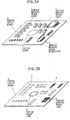
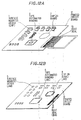
- Fig. 3A shows a PCB 12 mounted with electric elements thereon in the second preferred embodiment according to the invention, wherein like parts are indicated by like reference numerals as used in Figs. 1A and 2A.
- a COB device 7 (a pair of ICs) is provided on the PCB 12 in addition to the SMDs 1, 2 and 3.
- Figs. 3B and 3C show the PCB 12 having a through-hole (only in 3C), SMD lands 5 and a COB land 8, wherein the COB land 8 comprises a predetermined pattern of a copper foil 81, a non-electrolysis Ni-Au plate 82, and a soft Au plate 83.
- the pair of ICs are mounted on the PCB 12 by using Au bonding wires (not shown) to be bonded to the soft Au solder 83 of the COB land 8.
- the SMDs 1, 2 and 3 are mounted on the PCB 12 in the same manner as in Figs. 1A, 1B and 1C.
- Fig. 4A shows a PCB 12 mounted with electric elements thereon wherein like parts are indicated by like reference numerals as used in Figs. 1A, 2A and 3A.
- a heat-sealed connector 10 for connecting internal circuits on the PCB 12 to external circuits is provided on the PCB 12.
- Fig. 4B shows the PCB 12 having SMD lands 5 and a heat-seal land 11, wherein the heat seal connection is realized in accordance with local re-flow of non-electrolysis Ni-Au plate, as shown in Fig. 1C, functioning as a surface-treating layer by thermal pressing method using thermal setting adhesive.
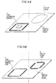
- Fig. 5A shows a PCB 12 mounted with electric elements thereon in the third preferred embodiment according to the invention, wherein like parts are indicated by like reference numerals as used in Figs. 1A to 4A.
- Fig. 5B shows the PCB 12 having a TAB land 6 and a COB land 8 which are explained before.
- Fig. 6A shows a PCB 12 mounted with electric elements thereon in the fourth preferred embodiment according to the invention, wherein like parts are indicated by like reference numerals as used in Figs. 1A to 5A.
- Fig. 6B shows the PCB 12 having a TAB land 6 and a heat-seal land 11 which are explained before.
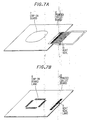
- Fig. 7A shows a PCB 12 mounted with electric elements thereon in the fifth preferred embodiment according to the invention, wherein like parts are indicated by like reference numerals as used in Figs. 1A to 6A.
- Fig. 7B shows the PCB 12 having a COB land 8 and a heat-seal land 11 which are explained before.
- Fig. 8A and 8B show a PCB 12 in the sixth preferred embodiment according to the invention, wherein a TAB package 4, a COB-IC 7, and a heat-sealed connector 10 are mounted on the PCB 12 by the OLB method using a tape carrier package, the COB method using Au bonding wires, and the thermal pressing method providing heat-seal, as described before.
- the TAB land 6 has an electrolysis solder plate
- the COB land 8 has a soft Ni-Au plate
- the heat seal land 11 has a non-electrolysis Ni-Au plate, respectively, as surface-treating layers.
- Figs. 9A and 9B show a PCB mounted with IC thereon in the seventh preferred embodiment according to the invention, wherein resistance and capacitor chips 1 and a connector 3, a TAB package 4, and a COB-IC 7 are mounted on the PCB 12 by the re-flow method using cream solder, the OLB method for mounting a tape carrier package, and the thermal pressing method providing heat-seal, respectively.
- the SMD lands 5 has a non-electrolysis Ni-Au plate
- the TAB land 6 has an electrolysis solder plate
- the COB land 8 has a soft Au plate, respectively, as surface-treating layers.
- Figs. 10A and 10B show a PCB mounted with electric elements thereon in the eighth preferred embodiment according to the invention, wherein resistance and capacitor chips 1 and a SOP 2, a TAB package 4 and a heat-sealed connector 10 are mounted on the PCB 12 by the re-flow method using cream solder, the OLB method for mounting a tap carrier package, and the thermal pressing method providing heat-seal, respectively.
- the SMD lands 5 and the heat-seal land 11 have non-electrolysis Ni-Au plates and the TAB land 6 has an electrolysis solder plate, respectively, as surface-treating layers.
- Figs. 11A and 11B show, a PCB mounted with electric elements thereon in the ninth preferred embodiment according to the invention, wherein resistance and capacitor chips 11, a SOP 2, a COB-IC 7, and a heat-sealed connector 10 are mounted on the PCB 12 by the re-flow method using cream solder, the COB method using Au bonding wires, and the thermal pressing method providing heat-seal, respectively.
- the SMD lands 5, and the heat-seal land 11 have non-electrolysis Ni-Au plates, and the COB land 8 has a soft Au plate, respectively, as surface-treating layers.
- Figs. 12A and 12B show a PCB mounted with electric elements thereon in the tenth preferred embodiment according to the invention, wherein resistance and capacitor chips 1, a TAB package 4, a COB-IC 7, and a heat-sealed connector 10 are mounted on the PCB 12 by the re-flow method using cream solder, the OLB method for mounting a tape carrier package, the COB method using Au bonding wires, and the thermal pressing method providing heat-seal, respectively.
- the SMD lands 5 and the heat-seal land 11 have non-electrolysis Ni-Au plates
- the TAB land 6 has an electrolysis solder plate
- the COB land 8 has a soft Au plate, respectively, as surface-treating layers.
Landscapes
- Engineering & Computer Science (AREA)
- Microelectronics & Electronic Packaging (AREA)
- Manufacturing & Machinery (AREA)
- Electric Connection Of Electric Components To Printed Circuits (AREA)
- Structures For Mounting Electric Components On Printed Circuit Boards (AREA)
- Wire Bonding (AREA)
Claims (3)
- Carte à circuit imprimé comportant des plages pour monter des éléments électriques sur la carte à circuit imprimé, caractérisé en ce que lesdites plages comportent au moins deux éléments parmi :(a) une plage (5 ; 11) à utiliser dans des procédés de compression thermique et par refusion pour monter des éléments électriques sur la carte à circuit imprimé, ladite plage comportant une partie (51) ayant un motif prédéterminé constituée d'une feuille de cuivre recouverte d'une couche formant plaque de Ni-Au non-électrolytique (52),(b) une plage (6) à utiliser dans un procédé de soudure des connexions extérieures pour monter des éléments électriques sur la carte à circuit imprimé, ladite plage comportant une partie (61) ayant ledit motif prédéterminé constituée d'une feuille de cuivre recouverte de ladite couche formant plaque de Ni-Au non-électrolytique (62), ladite couche formant plaque de Ni-Au étant à son tour recouverte d'une couche formant plaque de soudure électrolytique (63), et(c) une plage (8) à utiliser dans un procédé d'intégration sur carte pour monter des éléments électriques sur la carte à circuit imprimé, ladite plage comportant une partie (81) ayant ledit motif prédéterminé constituée d'une feuille de cuivre recouverte par ladite couche formant plaque de Ni-Au non-électrolytique (82), ladite couche formant plaque étant à son tour recouverte d'une couche formant plaque de Au doux (83).
- Carte à circuit imprimé selon la revendication 1, comportant une pluralité d'éléments électriques montés dessus, lesdits éléments électriques comportant au moins deux éléments électriques sélectionnés parmi une puce de résistance, une puce de condensateur, un boítier de dispositif à semi-conducteurs et un connecteur.
- Procédé de fabrication d'une carte à circuit imprimé comportant des plages (5, 6, 8, 11) pour monter des composants électriques sur la carte à circuit imprimé, lesdites plages comportant un motif prédéterminé d'une feuille de cuivre (51, 61, 81) recouverte d'une couche formant plaque de Ni-Au non-électrolytique (51, 62, 82) pour permettre aux éléments électriques d'être montés par des procédés de compression thermique et par refusion, sur les plages recouvertes par la couche formant plaque de Ni-Au, caractérisé en ce que ledit procédé comporte au moins une des étapes suivantes consistant a :recouvrir ladite couche formant plaque de Ni-Au non-électrolytique (62) sur certaines des plages (6) à l'aide d'une plaque de soudure électrolytique (63) pour permettre à des éléments électriques d'être montés par un procédé par refusion locale sur les plages (6) recouvertes par la couche formant plaque de soudure électrolytique (63), etrecouvrir ladite couche formant plaque de Ni-Au non-électrolytique (82) d'autres plages (8) avec une couche formant plaque de Au doux (83) pour permettre aux éléments électriques d'être montés par un procédé d'intégration sur carte, sur les plages (8) recouvertes par la couche formant plaque de Au doux (83).
Applications Claiming Priority (3)
| Application Number | Priority Date | Filing Date | Title |
|---|---|---|---|
| JP28263892 | 1992-10-21 | ||
| JP4282638A JP2783093B2 (ja) | 1992-10-21 | 1992-10-21 | プリント配線板 |
| JP282638/92 | 1992-10-21 |
Publications (3)
| Publication Number | Publication Date |
|---|---|
| EP0594427A2 EP0594427A2 (fr) | 1994-04-27 |
| EP0594427A3 EP0594427A3 (fr) | 1995-06-21 |
| EP0594427B1 true EP0594427B1 (fr) | 2000-02-02 |
Family
ID=17655125
Family Applications (1)
| Application Number | Title | Priority Date | Filing Date |
|---|---|---|---|
| EP93308379A Expired - Lifetime EP0594427B1 (fr) | 1992-10-21 | 1993-10-21 | Plaque à circuit imprimé avec des éléments électriques montés dessus |
Country Status (7)
| Country | Link |
|---|---|
| US (1) | US5400221A (fr) |
| EP (1) | EP0594427B1 (fr) |
| JP (1) | JP2783093B2 (fr) |
| KR (1) | KR0123032B1 (fr) |
| AU (1) | AU672433B2 (fr) |
| CA (1) | CA2108868C (fr) |
| DE (1) | DE69327765T2 (fr) |
Families Citing this family (27)
| Publication number | Priority date | Publication date | Assignee | Title |
|---|---|---|---|---|
| JP2606115B2 (ja) * | 1993-12-27 | 1997-04-30 | 日本電気株式会社 | 半導体実装基板用素子接合パッド |
| SE517185C2 (sv) * | 1993-12-28 | 2002-05-07 | Ericsson Telefon Ab L M | Komponentmodulanpassad oscillerande kretsanordning |
| US5523920A (en) * | 1994-01-03 | 1996-06-04 | Motorola, Inc. | Printed circuit board comprising elevated bond pads |
| US5799393A (en) * | 1994-11-09 | 1998-09-01 | Blaupunkt-Werke Gmbh | Method for producing a plated-through hole on a printed-circuit board |
| JPH08162745A (ja) * | 1994-12-01 | 1996-06-21 | Alps Electric Co Ltd | 電子部品の固定端子構造 |
| JP3231225B2 (ja) * | 1995-09-18 | 2001-11-19 | アルプス電気株式会社 | プリント配線基板 |
| WO1997046063A1 (fr) * | 1996-05-31 | 1997-12-04 | The Whitaker Corporation | Pattes de raccordement aux conducteurs d'une plaque de cablage pour circuit imprime a conducteurs |
| US5808877A (en) * | 1996-09-19 | 1998-09-15 | Samsung Electronics Co., Ltd. | Multichip package having exposed common pads |
| US5841686A (en) * | 1996-11-22 | 1998-11-24 | Ma Laboratories, Inc. | Dual-bank memory module with shared capacitors and R-C elements integrated into the module substrate |
| JP3489369B2 (ja) | 1997-01-31 | 2004-01-19 | 松下電器産業株式会社 | ゴキブリ忌避剤含有電子部品材料を用いた電子部品 |
| US5910644A (en) * | 1997-06-11 | 1999-06-08 | International Business Machines Corporation | Universal surface finish for DCA, SMT and pad on pad interconnections |
| JPH1154237A (ja) * | 1997-08-07 | 1999-02-26 | Yazaki Corp | 配線基板の放電構造 |
| US6326797B2 (en) | 1998-03-04 | 2001-12-04 | International Business Machines Corporation | Apparatus and method for evaluating printed circuit board assembly manufacturing processes |
| JP2000286526A (ja) * | 1999-03-30 | 2000-10-13 | Murata Mfg Co Ltd | 表面実装構造及びその表面実装構造に用いられる表面実装型電子部品 |
| DE10047897B4 (de) * | 2000-09-26 | 2008-04-24 | Patent-Treuhand-Gesellschaft für elektrische Glühlampen mbH | Elektronische Baueinheit mit einer als Leadframe ausgebildeten Montageplatte und darauf befestigten SMD-Bauteilen |
| JP2002359459A (ja) * | 2001-06-01 | 2002-12-13 | Nec Corp | 電子部品の実装方法、プリント配線基板および実装構造体 |
| US20040041520A1 (en) * | 2002-08-27 | 2004-03-04 | Ritdisplay Corporation | Panel for organic electroluminescent device |
| US7167375B2 (en) * | 2004-01-16 | 2007-01-23 | Motorola, Inc. | Populated printed wiring board and method of manufacture |
| US9793247B2 (en) | 2005-01-10 | 2017-10-17 | Cree, Inc. | Solid state lighting component |
| US9070850B2 (en) | 2007-10-31 | 2015-06-30 | Cree, Inc. | Light emitting diode package and method for fabricating same |
| TWI348341B (en) * | 2005-05-18 | 2011-09-01 | Chunghwa Picture Tubes Ltd | Electronic element module and electronic device using the same |
| JP4770514B2 (ja) * | 2006-02-27 | 2011-09-14 | 株式会社デンソー | 電子装置 |
| US10295147B2 (en) * | 2006-11-09 | 2019-05-21 | Cree, Inc. | LED array and method for fabricating same |
| US20110279990A1 (en) * | 2009-02-26 | 2011-11-17 | Makoto Hirano | Printed board and electronic equipment incorporating the printed board |
| US9786811B2 (en) | 2011-02-04 | 2017-10-10 | Cree, Inc. | Tilted emission LED array |
| US10842016B2 (en) | 2011-07-06 | 2020-11-17 | Cree, Inc. | Compact optically efficient solid state light source with integrated thermal management |
| US11033990B2 (en) * | 2018-11-29 | 2021-06-15 | Raytheon Company | Low cost approach for depositing solder and adhesives in a pattern for forming electronic assemblies |
Family Cites Families (14)
| Publication number | Priority date | Publication date | Assignee | Title |
|---|---|---|---|---|
| DE3136198A1 (de) * | 1981-01-15 | 1982-08-05 | Robert Bosch Gmbh, 7000 Stuttgart | "elektronische duennschichtschaltung" |
| US4447857A (en) * | 1981-12-09 | 1984-05-08 | International Business Machines Corporation | Substrate with multiple type connections |
| JPS5990938A (ja) * | 1982-11-17 | 1984-05-25 | Nec Corp | 半導体装置用プリント回路基板 |
| JPS63283033A (ja) * | 1987-05-15 | 1988-11-18 | Nec Corp | ダイボンディング方法 |
| FR2629272B1 (fr) * | 1988-03-22 | 1990-11-09 | Bull Sa | Support de circuit integre de haute densite et appareil d'etamage selectif des conducteurs du support |
| JPH01278032A (ja) * | 1988-04-28 | 1989-11-08 | Nec Kansai Ltd | ワイヤボンディング方法 |
| US5144535A (en) * | 1989-04-20 | 1992-09-01 | U.S. Philips Corporation | Method of mounting electrical and/or electronic components of a printed circuit board |
| CA2018208C (fr) * | 1989-06-16 | 1995-01-31 | Albert Ott | Methode de fabrication de cartes de circuits imprimes |
| JP2768448B2 (ja) * | 1989-12-27 | 1998-06-25 | 田中電子工業株式会社 | 半田バンプの形成方法 |
| JPH0451582A (ja) * | 1990-06-20 | 1992-02-20 | Nec Corp | 混成集積回路装置 |
| JPH04116837A (ja) * | 1990-09-06 | 1992-04-17 | Matsushita Electric Ind Co Ltd | 電子回路の表面実装方法 |
| US5270903A (en) * | 1990-09-10 | 1993-12-14 | Codex Corporation | Printed circuit board manufacturing method accommodates wave soldering and press fitting of components |
| JPH04225539A (ja) * | 1990-12-27 | 1992-08-14 | Seiko Instr Inc | 半導体装置の製造方法 |
| JPH04280663A (ja) * | 1991-03-08 | 1992-10-06 | Hitachi Ltd | 半導体装置およびその実装方法 |
-
1992
- 1992-10-21 JP JP4282638A patent/JP2783093B2/ja not_active Expired - Fee Related
-
1993
- 1993-10-20 CA CA002108868A patent/CA2108868C/fr not_active Expired - Fee Related
- 1993-10-21 US US08/139,084 patent/US5400221A/en not_active Expired - Lifetime
- 1993-10-21 KR KR93021910A patent/KR0123032B1/ko not_active Expired - Fee Related
- 1993-10-21 EP EP93308379A patent/EP0594427B1/fr not_active Expired - Lifetime
- 1993-10-21 DE DE69327765T patent/DE69327765T2/de not_active Expired - Fee Related
- 1993-10-21 AU AU49177/93A patent/AU672433B2/en not_active Ceased
Also Published As
| Publication number | Publication date |
|---|---|
| AU672433B2 (en) | 1996-10-03 |
| DE69327765D1 (de) | 2000-03-09 |
| KR0123032B1 (en) | 1997-11-22 |
| EP0594427A2 (fr) | 1994-04-27 |
| JPH06132626A (ja) | 1994-05-13 |
| CA2108868C (fr) | 1997-05-27 |
| CA2108868A1 (fr) | 1994-04-22 |
| AU4917793A (en) | 1994-05-05 |
| US5400221A (en) | 1995-03-21 |
| JP2783093B2 (ja) | 1998-08-06 |
| DE69327765T2 (de) | 2000-10-12 |
| EP0594427A3 (fr) | 1995-06-21 |
Similar Documents
| Publication | Publication Date | Title |
|---|---|---|
| EP0594427B1 (fr) | Plaque à circuit imprimé avec des éléments électriques montés dessus | |
| US5367435A (en) | Electronic package structure and method of making same | |
| US5433822A (en) | Method of manufacturing semiconductor device with copper core bumps | |
| US6504104B2 (en) | Flexible wiring for the transformation of a substrate with edge contacts into a ball grid array | |
| KR100231276B1 (ko) | 반도체패키지의 구조 및 제조방법 | |
| KR0141580B1 (ko) | 표면 설치가능 반도체 장치 | |
| EP1168447A2 (fr) | Dispositif semi- conducteur et methode | |
| EP0632685A2 (fr) | Assemblage pour les plaquettes élastiques de circuit avec dissipation commune de chaleur, procédé de fabrication | |
| US20020130411A1 (en) | Bga substrate via structure | |
| JP2001168233A (ja) | 多重回線グリッド・アレイ・パッケージ | |
| JPH04356998A (ja) | マルチチップモジュール | |
| JPH0193198A (ja) | 回路基板の製造方法 | |
| US20080032523A1 (en) | Circuit module and manufacturing process thereof | |
| KR20030011433A (ko) | 다층 인쇄회로기판의 숨겨진 레이저 비아홀 제조방법 | |
| JPH0821648B2 (ja) | 厚膜技術により形成されたピンレスグリッドアレイ電極構造 | |
| JPH08167676A (ja) | 半導体装置 | |
| KR19990002341A (ko) | 이형칩부품 혼재실장용 인쇄회로기판 및 그 제조방법 | |
| JP3692810B2 (ja) | 半導体装置及びその製造方法、回路基板並びに電子機器 | |
| KR200147513Y1 (ko) | 표면 실장형 반도체 패키지 | |
| JPH05327156A (ja) | プリント回路基板 | |
| KR100246848B1 (ko) | 랜드 그리드 어레이 및 이를 채용한 반도체 패키지 | |
| US6410860B2 (en) | Electronic circuit package assembly with solder interconnection sheet | |
| JPS5923432Y2 (ja) | 半導体装置 | |
| JPS6293993A (ja) | 電子回路装置とその実装方法 | |
| JPH10178122A (ja) | Ic搭載用多層プリント配線板 |
Legal Events
| Date | Code | Title | Description |
|---|---|---|---|
| PUAI | Public reference made under article 153(3) epc to a published international application that has entered the european phase |
Free format text: ORIGINAL CODE: 0009012 |
|
| AK | Designated contracting states |
Kind code of ref document: A2 Designated state(s): DE FR GB IT NL SE |
|
| PUAL | Search report despatched |
Free format text: ORIGINAL CODE: 0009013 |
|
| AK | Designated contracting states |
Kind code of ref document: A3 Designated state(s): DE FR GB IT NL SE |
|
| 17P | Request for examination filed |
Effective date: 19950522 |
|
| 17Q | First examination report despatched |
Effective date: 19980914 |
|
| GRAG | Despatch of communication of intention to grant |
Free format text: ORIGINAL CODE: EPIDOS AGRA |
|
| GRAG | Despatch of communication of intention to grant |
Free format text: ORIGINAL CODE: EPIDOS AGRA |
|
| GRAH | Despatch of communication of intention to grant a patent |
Free format text: ORIGINAL CODE: EPIDOS IGRA |
|
| GRAH | Despatch of communication of intention to grant a patent |
Free format text: ORIGINAL CODE: EPIDOS IGRA |
|
| GRAA | (expected) grant |
Free format text: ORIGINAL CODE: 0009210 |
|
| AK | Designated contracting states |
Kind code of ref document: B1 Designated state(s): DE FR GB IT NL SE |
|
| REF | Corresponds to: |
Ref document number: 69327765 Country of ref document: DE Date of ref document: 20000309 |
|
| ITF | It: translation for a ep patent filed | ||
| ET | Fr: translation filed | ||
| PGFP | Annual fee paid to national office [announced via postgrant information from national office to epo] |
Ref country code: NL Payment date: 20001026 Year of fee payment: 8 |
|
| PLBE | No opposition filed within time limit |
Free format text: ORIGINAL CODE: 0009261 |
|
| 26N | No opposition filed | ||
| REG | Reference to a national code |
Ref country code: GB Ref legal event code: IF02 |
|
| PG25 | Lapsed in a contracting state [announced via postgrant information from national office to epo] |
Ref country code: NL Free format text: LAPSE BECAUSE OF NON-PAYMENT OF DUE FEES Effective date: 20020501 |
|
| NLV4 | Nl: lapsed or anulled due to non-payment of the annual fee |
Effective date: 20020501 |
|
| PGFP | Annual fee paid to national office [announced via postgrant information from national office to epo] |
Ref country code: SE Payment date: 20041006 Year of fee payment: 12 |
|
| PG25 | Lapsed in a contracting state [announced via postgrant information from national office to epo] |
Ref country code: SE Free format text: LAPSE BECAUSE OF NON-PAYMENT OF DUE FEES Effective date: 20051022 |
|
| EUG | Se: european patent has lapsed | ||
| PGFP | Annual fee paid to national office [announced via postgrant information from national office to epo] |
Ref country code: DE Payment date: 20071018 Year of fee payment: 15 |
|
| PGFP | Annual fee paid to national office [announced via postgrant information from national office to epo] |
Ref country code: IT Payment date: 20071026 Year of fee payment: 15 |
|
| PGFP | Annual fee paid to national office [announced via postgrant information from national office to epo] |
Ref country code: GB Payment date: 20071017 Year of fee payment: 15 Ref country code: FR Payment date: 20071009 Year of fee payment: 15 |
|
| GBPC | Gb: european patent ceased through non-payment of renewal fee |
Effective date: 20081021 |
|
| REG | Reference to a national code |
Ref country code: FR Ref legal event code: ST Effective date: 20090630 |
|
| PG25 | Lapsed in a contracting state [announced via postgrant information from national office to epo] |
Ref country code: IT Free format text: LAPSE BECAUSE OF NON-PAYMENT OF DUE FEES Effective date: 20081021 Ref country code: DE Free format text: LAPSE BECAUSE OF NON-PAYMENT OF DUE FEES Effective date: 20090501 |
|
| PG25 | Lapsed in a contracting state [announced via postgrant information from national office to epo] |
Ref country code: FR Free format text: LAPSE BECAUSE OF NON-PAYMENT OF DUE FEES Effective date: 20081031 |
|
| PG25 | Lapsed in a contracting state [announced via postgrant information from national office to epo] |
Ref country code: GB Free format text: LAPSE BECAUSE OF NON-PAYMENT OF DUE FEES Effective date: 20081021 |