EP0595155A2 - Dispositif d'affichage à cristal liquide - Google Patents
Dispositif d'affichage à cristal liquide Download PDFInfo
- Publication number
- EP0595155A2 EP0595155A2 EP93116808A EP93116808A EP0595155A2 EP 0595155 A2 EP0595155 A2 EP 0595155A2 EP 93116808 A EP93116808 A EP 93116808A EP 93116808 A EP93116808 A EP 93116808A EP 0595155 A2 EP0595155 A2 EP 0595155A2
- Authority
- EP
- European Patent Office
- Prior art keywords
- pixel
- liquid crystal
- cell thickness
- pair
- electrodes
- Prior art date
- Legal status (The legal status is an assumption and is not a legal conclusion. Google has not performed a legal analysis and makes no representation as to the accuracy of the status listed.)
- Granted
Links
Images


Classifications
-
- G—PHYSICS
- G02—OPTICS
- G02F—OPTICAL DEVICES OR ARRANGEMENTS FOR THE CONTROL OF LIGHT BY MODIFICATION OF THE OPTICAL PROPERTIES OF THE MEDIA OF THE ELEMENTS INVOLVED THEREIN; NON-LINEAR OPTICS; FREQUENCY-CHANGING OF LIGHT; OPTICAL LOGIC ELEMENTS; OPTICAL ANALOGUE/DIGITAL CONVERTERS
- G02F1/00—Devices or arrangements for the control of the intensity, colour, phase, polarisation or direction of light arriving from an independent light source, e.g. switching, gating or modulating; Non-linear optics
- G02F1/01—Devices or arrangements for the control of the intensity, colour, phase, polarisation or direction of light arriving from an independent light source, e.g. switching, gating or modulating; Non-linear optics for the control of the intensity, phase, polarisation or colour
- G02F1/13—Devices or arrangements for the control of the intensity, colour, phase, polarisation or direction of light arriving from an independent light source, e.g. switching, gating or modulating; Non-linear optics for the control of the intensity, phase, polarisation or colour based on liquid crystals, e.g. single liquid crystal display cells
- G02F1/133—Constructional arrangements; Operation of liquid crystal cells; Circuit arrangements
- G02F1/1333—Constructional arrangements; Manufacturing methods
- G02F1/1335—Structural association of cells with optical devices, e.g. polarisers or reflectors
- G02F1/133509—Filters, e.g. light shielding masks
- G02F1/133514—Colour filters
-
- G—PHYSICS
- G02—OPTICS
- G02F—OPTICAL DEVICES OR ARRANGEMENTS FOR THE CONTROL OF LIGHT BY MODIFICATION OF THE OPTICAL PROPERTIES OF THE MEDIA OF THE ELEMENTS INVOLVED THEREIN; NON-LINEAR OPTICS; FREQUENCY-CHANGING OF LIGHT; OPTICAL LOGIC ELEMENTS; OPTICAL ANALOGUE/DIGITAL CONVERTERS
- G02F1/00—Devices or arrangements for the control of the intensity, colour, phase, polarisation or direction of light arriving from an independent light source, e.g. switching, gating or modulating; Non-linear optics
- G02F1/01—Devices or arrangements for the control of the intensity, colour, phase, polarisation or direction of light arriving from an independent light source, e.g. switching, gating or modulating; Non-linear optics for the control of the intensity, phase, polarisation or colour
- G02F1/13—Devices or arrangements for the control of the intensity, colour, phase, polarisation or direction of light arriving from an independent light source, e.g. switching, gating or modulating; Non-linear optics for the control of the intensity, phase, polarisation or colour based on liquid crystals, e.g. single liquid crystal display cells
- G02F1/133—Constructional arrangements; Operation of liquid crystal cells; Circuit arrangements
- G02F1/1333—Constructional arrangements; Manufacturing methods
- G02F1/1343—Electrodes
- G02F1/134309—Electrodes characterised by their geometrical arrangement
- G02F1/134336—Matrix
-
- G—PHYSICS
- G02—OPTICS
- G02F—OPTICAL DEVICES OR ARRANGEMENTS FOR THE CONTROL OF LIGHT BY MODIFICATION OF THE OPTICAL PROPERTIES OF THE MEDIA OF THE ELEMENTS INVOLVED THEREIN; NON-LINEAR OPTICS; FREQUENCY-CHANGING OF LIGHT; OPTICAL LOGIC ELEMENTS; OPTICAL ANALOGUE/DIGITAL CONVERTERS
- G02F1/00—Devices or arrangements for the control of the intensity, colour, phase, polarisation or direction of light arriving from an independent light source, e.g. switching, gating or modulating; Non-linear optics
- G02F1/01—Devices or arrangements for the control of the intensity, colour, phase, polarisation or direction of light arriving from an independent light source, e.g. switching, gating or modulating; Non-linear optics for the control of the intensity, phase, polarisation or colour
- G02F1/13—Devices or arrangements for the control of the intensity, colour, phase, polarisation or direction of light arriving from an independent light source, e.g. switching, gating or modulating; Non-linear optics for the control of the intensity, phase, polarisation or colour based on liquid crystals, e.g. single liquid crystal display cells
- G02F1/133—Constructional arrangements; Operation of liquid crystal cells; Circuit arrangements
- G02F1/1333—Constructional arrangements; Manufacturing methods
- G02F1/133371—Cells with varying thickness of the liquid crystal layer
-
- G—PHYSICS
- G02—OPTICS
- G02F—OPTICAL DEVICES OR ARRANGEMENTS FOR THE CONTROL OF LIGHT BY MODIFICATION OF THE OPTICAL PROPERTIES OF THE MEDIA OF THE ELEMENTS INVOLVED THEREIN; NON-LINEAR OPTICS; FREQUENCY-CHANGING OF LIGHT; OPTICAL LOGIC ELEMENTS; OPTICAL ANALOGUE/DIGITAL CONVERTERS
- G02F2203/00—Function characteristic
- G02F2203/30—Gray scale
Definitions
- the present invention relates to a liquid crystal display device for use in display apparatus for computer terminals, television receivers, word processors, typewriters, etc., a light valve for projectors, a view finder for video camera recorders, etc.
- liquid crystal display devices including those using twisted-nematic (TN) liquid crystals, quest-host-type liquid crystals, smectic (Sm) liquid crystals, etc.
- TN twisted-nematic
- Sm smectic
- Such a liquid crystal is disposed between a pair of substrates and changes an optical transmittance therethrough depending on voltages applied thereto.
- the method there are formed regions of a liquid crystal layer having different thicknesses in a unit pixel so as to apply different electric field intensities to the liquid crystal layer depending on the regions even when an identical voltage is supplied.
- the method is applicable not only to a TN liquid crystal but also to a ferroelectric liquid crystal (FLC) to effect a good gradational or grey-scale display.
- FLC ferroelectric liquid crystal
- An object of the present invention is to provide a liquid crystal display device having solved the above-mentioned technical problem and capable of effecting good image display.
- Another object of the present invention is to provide a liquid crystal display device having different electrode areas corresponding to different liquid crystal layer thicknesses.
- a further object of the present invention is to provide a liquid crystal display device having different characteristics and/or shapes of color filters corresponding to different liquid crystal layer thicknesses.
- a liquid crystal display device comprising: a pair of electrode plates disposed opposite to each other and each having at least one electrode on an opposite side thereof, and a liquid crystal disposed between the electrode plates, so as to form a plurality of pixels each comprising the liquid crystal and a pair of electrodes sandwiching the liquid crystal, wherein at least one electrode plate is provided with plural types of filters disposed corresponding to pixels, so that pixels corresponding to different types of filters are formed in different areas.
- a liquid crystal display device comprising: a pair of electrode plates disposed opposite to each other and each having at least one electrode on an opposite side thereof, and a layer of liquid crystal disposed between the electrode plates, so as to form a plurality of pixels each comprising the liquid crystal and a pair of electrodes sandwiching the liquid crystal, wherein the liquid crystal layer within a pixel is caused to have different thicknesses and the shape of the pixel is varied corresponding to the different thicknesses.
- Figures 1A - 1E are graphs showing spectral transmittance characteristics of optical means used in a liquid crystal display device according to the invention.
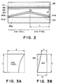
- Figure 2 is a schematic sectional view of a liquid crystal cell used in a liquid crystal display device according to the invention.
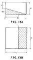
- Figures 3A and 3B are schematic views for describing a basic design concept regarding pixel structure according to the invention.
- Figures 4A and 4B are schematic views for describing a pixel structure according to the invention.
- Figures 5A an 5B are graphs illustrating a relationship between a switching pulse voltage and a transmitted light quantity.
- Figures 6A - 6D illustrate of pixels showing various transmittance levels depending on applied pulse voltage.
- Figure 7 is a graph for describing a deviation in threshold characteristic due to a temperature distribution.
- Figure 8 is a time chart for describing a four-pulse method.
- Figure 9 is an illustration of pixels showing various transmittance levels.
- Figure 10 is a schematic illustration of pixel structures in Example 1.
- Figure 11 is a schematic illustration of pixel structures in Example 2.
- Figures 12A and 12B are schematic illustrations for describing modifications of Example 2.
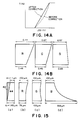
- Figures 13A and 13B are a schematic sectional view and a schematic plan view of a pixel used in Example 3.
- Figure 14A is a graph showing a change in T-V characteristic according to correction in Example 3, and Figure 14B is an illustration of a pixel structure used therefor.
- Figure 15 is an illustration of a pixel structure used in a liquid crystal device of Example 4.
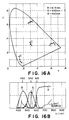
- Figures 16A and 16B are a chromaticity diagram and a spectral characteristic diagram for describing a liquid crystal device of Example 4.
- Figures 17A - 17C are schematic illustrations of display states at pixels in Example 4.
- Figure 18 is an illustration of ai pixel structure used in Example 5.
- Figure 19 is a chromaticity diagram for describing a liquid crystal device of Example 5.
- Figures 20A - 20C are schematic illustrations of display states at pixels in Example 4.
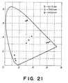
- Figure 21 is achromaticity diagram for illustrating a modification of Example 21.
- Figure 22 is a drive system block diagram of a liquid crystal display apparatus according to the invention.
- a deviation in transmittance through a pixel in a halftone display is corrected by modifying the areas of regions in the pixel.
- Such a pixel is ordinarily defined as a combination of an overlapping portion of electrodes respectively disposed on a pair of electrode plates, and a filter and/or a masking member disposed according to necessity.
- a specific wavelength fraction of light relatively easily transmitted can vary depending on the liquid crystal layer thickness (i.e., a so-called cell thickness) d .
- Figures 1A - 1E are graphs showing spectral characteristics of liquid crystal cells, a color filter, an optical filter and a light source, respectively.
- Figures 1A and 1B show liquid crystal cells having liquid crystal layer thicknesses (cell thicknesses) of 1.0 ⁇ m and 1.5 ⁇ m, respectively.
- a ferroelectric liquid crystal has a refractive index anisotropy ⁇ n in the range of about 0.15 - 0.19.
- Figure 3A shows a higher transmittance at a wavelength ( ⁇ ) of about 400 nm and a low transmittance in the neighborhood of 650 nm.
- the transmittance at about 400 nm is lowered but the transmittance at about 650 nm is increased.
- Table 1 R 650 nm G 540 nm B 400 nm FIG. 1A 1 a b FIG. 1B c d e
- the transmitted light quantities may be identical to each other for the respective wavelengths.
- Table 2 R 650 nm G 540 nm B 400 nm FIG. 1A 1 1/a 1/b FIG. 1B 1/c 1/d 1/e
- Figure 2 schematically illustrates a section corresponding to two pixels of a liquid crystal cell according to the invention.
- an electrode 41, an insulating film 42 and an alignment film 43 are disposed in flat layers on one substrate 45.
- a member 40 providing sloping surfaces is disposed, and thereon, electrodes 41a are formed for the respective pixels and are coated with an alignment film 43a.
- the electrode 41 on the upper substrate 45 are disposed common to the two pixels.
- the cell thickness in a pixel shown in Figure 2 varies continuously from d1 to d2 in a surface direction on the substrate and, if the relative area at each cell thickness d i (d1 ⁇ d i ⁇ d2) is standardized so as to provide an identical transmitted light intensity corresponding to the cell thickness d i , the above-mentioned phenomenon of varying transmitted light quantities due to varying cell thicknesses can be obviated.
- Figures 3A and 3B are schematic views showing a set of a pixel pattern and a cell thickness distribution in a pixel.
- a pixel has been provided in a rectangular pattern as represented by a dotted line in Figure 3A.
- the pixel width l is varied in the direction of cell thickness gradient, i.e., L direction.
- L direction the direction of cell thickness gradient
- the pixel area may be varied in several manners.
- Figures 4A and 4B show typical examples thereof. In these figures, only two pixels are shown for example, but a large display picture area may generally be composed of at least 100 pixels.
- Figure 4A shows a pixel pattern wherein one-side electrode 41 is provided with a lack based on the above-mentioned design concept. Of course such a lack can alternatively provided to the other side electrode 41a, or the both sides of electrodes 41 and 41a.
- Figure 4B shows an example wherein electrodes 41 and 41a are free from lacks but a filter (FT) disposed in superposition at a pixel is provided with a lack based on the above concept.
- the lack may be composed by a masking member BM as shown.
- FT filter
- the liquid crystal used in the present invention may be selected from known TN-liquid crystals, ferroelectric liquid crystals, anti-ferroelectric liquid crystals, etc.
- TN-liquid crystals inclusive of Schiff base-type liquid crystals such as alkoxybenzylidene alkylaniline and alkylalkoxyazobenzene, phenylbenzoate-type liquid crystals, cyanobiphenyl-type liquid crystals, cyclohexylcarboxylic acid ester liquid crystals, and 2,3-difluorophenylene-type liquid crystals
- smectic liquid crystals such as DOBAMBC and HOBACPC.
- the electrodes 41 and 41a used in the present invention may comprise a transparent conductor film such as that of tin oxide, indium tin oxide and indium tin oxide, which may be locally supplemented with a metal conductive film according to necessity for lowering the resistance.
- the member 40 for providing an unevenness so as to cause a cell thickness distribution in a pixel may be composed of an optically transparent resin or inorganic material.
- Gradational display may be performed by driving methods as disclosed in, e.g., U.S. Patents Nos. 4,747,671, 4,796,980, and 4,712,877.
- a ferroelectric liquid crystal has a spontaneous polarization so that a coupling force between the spontaneous polarization and an external electric field can be utilized for switching.
- the long axis direction of a ferroelectric liquid crystal molecule corresponds to the direction of the spontaneous polarization in a one-to-one relationship so that the switching is effected by the polarity of the external electric field.
- a ferroelectric liquid crystal generally comprises a chiral smectic liquid crystal (SmC* or SmH*), of which molecular long axes form helixes in the bulk state of the liquid crystal. If the chiral smectic liquid crystal is disposed within a cell having a small gap of about 1 - 3 ⁇ m as described above, the helixes of liquid crystal molecular long axes are unwound. This phenomenon is reported in, e.g., N.A. Clark, et al., MCLC (1983), Vol. 94, p.p. 213 - 234.
- a ferroelectric liquid crystal has been principally used in a binary (bright-dark) display device in which two stable states of the liquid crystal are used as a light-transmitting state and a light-interrupting state but can be used to effect a multi-value display, i.e., a halftone display.
- a halftone display method the areal ratio between bistable states (light transmitting state and light-interrupting state) within a pixel is controlled to realize an intermediate light-transmitting state.
- the gradational display method of this type hereinafter referred to as an "areal modulation" method
- Figure 5 is a graph schematically representing a relationship between a transmitted light quantity I through a ferroelectric liquid crystal cell and a switching pulse voltage V. More specifically, Figure 5A shows plots of transmitted light quantities I given by a pixel versus voltages V when the pixel initially placed in a complete light-interrupting (dark) state is supplied with single pulses of various voltages V and one polarity as shown in Figure 5B. When a pulse voltage V is below threshold Vth (V ⁇ Vth), the transmitted light quantity does not change and the pixel state is as shown in Figure 6B which is not different from the state shown in Figure 6A before the application of the pulse voltage.
- Vth threshold Vth
- the pulse voltage V exceeds the threshold Vth (V > Vth)
- a portion of the pixel is switched to the other stable state, thus being transitioned to a pixel state as shown in Figure 6C showing an intermediate transmitted light quantity as a whole.
- the pulse voltage V is further increased to exceed a saturation value Vsat (Vsat ⁇ V)
- the entire pixel is switched to a light-transmitting state as shown in Figure 6D so that the transmitted light quantity reaches a constant value (i.e., is saturated).
- the pulse voltage V applied to a pixel is controlled within a range of Vth ⁇ V ⁇ Vsat to display a halftone corresponding to the pulse voltage.
- the voltage (V) - transmitted light quantity (I) relationship shown in Figure 5 depends on the cell thickness and temperature. Accordingly, if a display panel is accompanied with an unintended cell thickness distribution or a temperature distribution, the display panel can display locally different gradation levels in response to a pulse voltage having a constant voltage.
- Figure 7 is a graph for illustrating the above phenomenon which is a graph showing a relationship between pulse voltage (V) and transmitted light quantity (I) similar to that shown in Figure 5 but showing two curves including a curve H representing a relationship at a high temperature and a curve L at a low temperature.
- V pulse voltage
- I transmitted light quantity
- Q0, Q0', Q1, Q2 and Q3 in Figure 9 represent gradation levels of a pixel, inclusive of Q0 representing black (0 %) and Q0' representing white (100 %).
- Each pixel in Figure 9 is provided with a threshold distribution within the pixel increasing from the leftside toward the right side as represented by a cell thickness increase.
- Such drive methods are effective in drive of a liquid crystal device having pixels each provided with a uniform threshold distribution therein as given by a cell thickness gradient as shown in Figure 2.
- a specific wavelength fraction of light relatively easily transmitted can vary depending on the liquid crystal layer thickness (i.e., a so-called cell thickness) d .
- the change in preferentially transmitted wavelength due to a change in cell thickness causes a change in central transmission wavelength at an identical gradational display level due to a temperature change, thus causing a coloration due to a temperature variation.
- transmittances at wavelengths of three primary colors are caused to vary depending on the temperature, so that a color obtained by combining these primary colors is also changed.
- tristimulus values e.g., R, G and B
- the measure of varying the electrode area depending on the cell thickness gradient thus providing a constant transmitted quantity at different cell thicknesses.
- the electrode area is made relatively large at a small cell thickness and is made relatively small at a large cell thickness, thereby allowing a better gradational display.
- the control of color filter areas may be performed for the respective color filters depending on the cell thickness.
- the color filter areas may be varied depending on the cell thickness in such a manner that red (R) and green (G) filter areas are made relatively large at a small cell thickness than at a large cell thickness, and a blue filter area is made relatively large at a large cell thickness and relatively small at a small cell thickness.
- the respective color filters are controlled with respect to entire areal sizes so as to equalize the transmittances through a liquid crystal layer at respective gradation levels, thus minimizing the deviation of color balance depending on gradation levels.
- the pixel shift method, etc. a change in color (particularly in color obtained by combination of R, G and B) due to a temperature change can be minimized.
- correction of transmitted light quantity was performed by using a cell having a cell thickness gradient in a pixel as shown in Figure 2.
- the smallest cell thickness d1 was set to 1.0 ⁇ m
- the largest cell thickness d2 was set to 1.40 ⁇ m
- the pixel width L was set to 200 ⁇ m.
- the electrodes 41a formed on the slope-providing unevenness members 40 and extending perpendicularly to the drawing were used as scanning electrodes.
- a UV (ultraviolet)-curable resin layer was formed on a glass substrate 45a and a mold having an uneven surface was pressed against thereto. In this state, the UV-curable resin layer was exposed to UV rays to form a cured resin layer 40 having an unevenness pattern forming sloping sides was formed on the substrate 45a.
- the thus formed uneven substrate 45a (with 40) and another glass substrate 45 were respectively coated with ITO films (sheet resistivity of about 30 ⁇ -square), which were then patterned into electrodes 41a and 41, respectively.
- the electrodes 41a and 41 on both substrates 40a and 40 were coated with about 400 ⁇ -thick polyimide alignment films 43a and 43 (formed by application and curing of a polyimide-forming liquid ("LQ-1802", mfd. by Hitachi Kasei K.K.)), which were then rubbed in a substantially identical direction substantially perpendicular to the extension of the scanning electrodes 41a.
- Table 4 shows a table of transmittances per unit area of the cell at various cell thicknesses and at central wavelengths (610 nm, 545 nm and 435 nm) of a three wavelength-fluorescent tube showing a spectral characteristic as shown in Figure 1E when illuminated with the fluorescent tube as the light source.
- the transmittances in Table 4 are shown in relative values with the transmittance at a cell thickness of 0.8 ⁇ m for light having a wavelength of 610 nm as the reference (i.e., 1).
- the transmittances in Table 4 are values per unit area and, at parts having different transmittances, transmitted light quantities are caused to be different.
- the values in parentheses in Table 4 are reciprocals of the transmittances and represent areal ratios (relative areas) for providing identical transmitted quantities for solving the above problem.
- the pixel portion areas at various thicknesses may suitably be constituted in areal ratios which are reciprocals of the transmittances at the respective thicknesses.
- the length L in a direction accompanied with a cell thickness gradient is fixed as shown in Figure 3A, so that the portions of the pixel at various thicknesses may be changed by varying the electrode width l .
- the color filters used herein had central wavelengths which were identical to those of the three-wavelength tube shown in Table 4.
- the electrode widths of electrodes with respective filters were determined at respective cell thickness portions so as to have areal ratios shown in Table 4.
- the electrode with an R filter was caused to have a width changing from 142 ⁇ m to 98 ⁇ m within one pixel corresponding to the cell thickness change.
- the electrodes with G and B filters were also set to have widths changing from 124 ⁇ m to 92 ⁇ m (G) and from 98 ⁇ m to 98 ⁇ m (B).
- the transmitted light quantity through each pixel was made identical even at different cell thickness portions and was also made identical to three types of pixels, thereby realizing a good color display.
- Table 5 shows a table of transmittances per unit area of the cell at various cell thicknesses and at central wavelengths (610 nm, 545 nm and 435 nm) of a three wavelength-fluorescent tube showing a spectral characteristic as used in Example 1 when illuminated with the fluorescent tube as the light source.
- the transmittances in Table 5 are shown in relative values with the transmittance at a cell thickness of 0.8 ⁇ m for light having a wavelength of 610 nm as the reference (i.e., 1).
- the transmittances in Table 5 are values per unit area and, at parts having different transmittances, transmitted light quantities are caused to be different.
- the values in parentheses in Table 5 are reciprocals of the transmittances and represent areal ratios (relative areas) for providing identical transmitted quantities for solving the above problem.
- the pixel portion areas at various thicknesses may suitably be constituted in areal ratios which are reciprocals of the transmittances at the respective thicknesses.
- the length L in a direction accompanied with a cell thickness gradient is fixed as shown in Figure 3A, so that the portions of the pixel at various thicknesses may be changed by varying the electrode width l .
- the color filters used herein had central wavelengths which were identical to those of the three-wavelength tube shown in Table 5.
- the electrode widths of electrodes with respective filters were determined at respective cell thickness portions so as to have areal ratios shown in Table 5.
- the electrode with an R filter was caused to have a width changing from 126 ⁇ m to 92 ⁇ m within one pixel corresponding to the cell thickness change.
- the electrodes with G and B filters were also set to have widths changing from 110 ⁇ m to 94 ⁇ m (G) and from 94 ⁇ m to 130 ⁇ m (B).
- the decrease in aperture rate according to the arrangement shown in Figure 12A given by a cell thickness change in the range of 1.1 ⁇ m - 1.65 ⁇ m was 2.1 % compared with that in the case of no electrode change.
- the decrease in aperture rate according to an arrangement shown in Figure 12 given by a cell thickness change in the range of 1.0 ⁇ m - 1.40 ⁇ m was 10.4 %.
- an inverted area in a pixel is proportional to an applied voltage V.
- an electric field intensity required for causing an inversion of a ferroelectric liquid crystal is denoted by Eth
- This formula represents a linear V - T relationship on a graph represented with T and V taken linearly scaled ordinate and abscissa.
- Eth'/Eth constitutes a constant term independent of V and is included in the constant C.
- T-log V retains a constant slope without depending on a temperature change.
- Figure 14(a) shows a T-V characteristic curve.
- a linear relationship is not attained as represented by a dashed line (before correction) in Figure 14A plotted on a log V abscissa.
- the electrode width l shown in Figure 3 is appropriately changed depending on the cell thickness gradient as described with reference to Table 6 blow, a linear relationship as represented by a solid line (after correction) shown in Figure 14A can be established.
- the relationship between the input voltage and the position (x) at a pixel shown in Table 6 is linear as represented by the above formula (I).
- the transmittance before correction and the input voltage or the position (x) is also linear. However, if the electrode widths at the respective positions are multiplied by corresponding electrode width ratio (correction factors) in Table 6, the transmittances after correction show a logarithmic relationship (i.e., linear T-log V relationship).
- the transmitted light quantity can be made identical regardless of the cell thickness as explained within Examples 1 and 2. If the electrode width is further modified by factors shown in Table 6, a T-V characteristic allowing a parallel shift on a log. V scale abscissa is obtained.
- Figure 14B shows patterns of electrodes for R, G and B with their relative sizes.
- the correction is made to a T-V characteristic but the same correction can be applied to a transmittance (T) - pulse width ( ⁇ T) for expressing a gradation characteristic by taking log ( ⁇ T) on the abscissa.
- Table 7 shows a table of transmittances per unit area of the cell at various cell thicknesses and at peak wavelengths (615 nm, 540 nm and 450 nm) of a light transmitted through the respective pixels of R, G and B.
- the transmittances in Table 7 are shown in relative values with the transmittance at a cell thickness of 1.1 ⁇ m for light having a wavelength of 615 nm as the reference (i.e., 1).
- a liquid crystal cell constituted in this manner was driven according to the four pulse method while changing the temperature, and the resultant pixel states were observed through a microscope. Examples of the pixel states thus observed are illustrated in Figures 17A - 17C.
- the transmissive state portions were formed at a relatively small cell thickness as shown in Figure 17A.
- the transmissive state portions were formed at a relatively large cell thickness as shown in Figure 17C.
- the R, G and B pixels were turned on one by one and all simultaneously, and the resultant colors were measured by a colorimeter.
- Figure 16A shows traces of color changes on a chromaticity diagram in the case of such a most noticeable change during the above experiment.
- the coordinate points A represent the case of a transmissive portion at a narrow width formed at a low temperature
- the coordinate points C represent the case of a transmissive portion at a thick width formed at a high temperature.
- This example is directed to an improvement in display characteristic in a system wherein a gradational display is effected by distributing a cell thickness distribution within a pixel so as to form a distribution of electric field intensity applied to a liquid crystal layer within the pixel.
- a cell thickness distribution i.e., a liquid crystal layer thickness distribution
- transmitted light intensity through the liquid crystal layer can vary depending on the wavelength.
- the shapes of color filters were modified depending on the cell thicknesses so as to provide constant transmitted light quantities regardless of the cell thickness change for the respective color filters of R, G and B.
- the light source or color filters are not constituted to issue or transmitted monochromatic light.
- a light quantity (LL) sensible by human eyes is a quantity obtained by integrating a product of a transmitted light ⁇ ( ⁇ ) through a liquid crystal cell and a visual sensitivity ⁇ ( ⁇ ) of human eyes at respective wavelengths in the wavelength regions of the respective color filters (e.g., 380 nm - 780 nm).
- the transmitted light quantity at a certain wavelength is made constant regardless of the cell thickness as in Example 1, the sensible light quantity (LL) can be changed depending on the cell thickness.
- Table 8 shows a table of sensible light quantities (LL) per unit area of the cell at various cell thicknesses of light issued from the light source and transmitted through the respective color filters (represented by R, G and B together with their peak wavelengths).
- the sensible light quantities (LL) in Table 8 are shown in relative values with the quantity (LL) at a cell thickness of 1.1 ⁇ m transmitted through a pixel with an R filter as the reference (i.e., 1).
- a liquid crystal cell constituted in this manner was driven according to the four pulse method while changing the temperature, and the resultant pixel states were observed through a microscope. Examples of the pixel states thus observed are illustrated in Figures 20A - 20C.
- the transmissive state portions were formed at a relatively small cell thickness as shown in Figure 20A.
- the transmissive state portions were formed at a relatively large cell thickness.
- the R, G and B pixels were turned on one by one and all simultaneously, and the resultant colors were measured by a colorimeter. The color change due to the position of transmissive portions was most noticeable when the transmissive portions were narrow.
- Figure 19A shows traces of color changes on a chromaticity diagram in the case of such a most noticeable change during the above experiment.
- the coordinate points A represent the case of a transmissive portion at a narrow width formed at a low temperature
- the coordinate points C represent the case of a transmissive portion at a thick width formed at a high temperature.
- Figure 9 shows that the hue A given by a portion at a small thickness and the hue C at a large cell thickness were different from each other.
- An improvement to this problem may be given (i) by applying a white clear-black write sequence and a black clear-white sequence alternately to every other scanning line or (ii) by applying a white clear-black write sequence and a black clear-white write sequence to each scanning line in every other frame (vertical scanning). If such a drive scheme is effected, for writing a 10 % "white” state for example, the case of writing the 10 % "white” portion at a small cell thickness portion and the case of writing the 10 % "white” portion at a large cell thickness portion is averaged positionally (i) or with time (ii), whereby substantially no difference (difference between + mark and o mark in Figure 21) is left as shown in Figure 1.
- Figure 21 is a block diagram of drive system for a display apparatus according to an embodiment of the present invention.
- Scanning lines of a liquid crystal device 141 constituting a display panel are connected to a common-side drive IC 146 as a means for selecting a scanning line and applying thereto a selection signal and data lines are connected to a segment-side drive IC 143 as a means for applying gradation data signals.
- Image data from an image data generator 148 are divided by a controller 149 into common-side signals and segment side signals, which are then supplied to a common-side circuit and a segment-side circuit, respectively.
- scanning signals are produced by a shift register 147 and the drive IC 146 based on reference voltages distributed by an analog switch in a drive power supply unit 142.
- digital gradation signals supplied through a shift register 145 and a latch circuit 144 are converted into analog signals by a D/A converter in the drive IC 143 and supplied to the data lines.
- a D/A converter in the drive IC 143 For example, four bit digital signals may be converted into 24, i.e., 16 different analog signals.
- digital signals are latched before conversion into analog signals.
- a liquid crystal display device is constituted by a pair of electrode plates each having a plurality of elongated electrodes, and a layer of ferroelectric liquid crystal disposed between the electrode plates so as to form a pixel at each intersection of elongated electrodes disposed respectively on the pair of electrodes plates.
- At least one electrode plate is provided with an unevenness at each pixel so as to form a cell thickness gradient within each pixel, and at least one electrode plate is provided with at least three types of color filters each corresponding to a pixel.
- each color filter and/or each pixel is set to have an area and/or a shape varying depending on a local cell thickness so that light quantities or sensible light quantities transmitted through the respective filters and the liquid crystal layer are identical to each other regardless of the type of color filter.
- a similar pixel pattern deformation is effective for providing a linear T (transmittance) - log V (voltage) characteristic. Color pixels pattern deformation may preferably be effected in a complementary manner with respect to different colors.
Landscapes
- Physics & Mathematics (AREA)
- Nonlinear Science (AREA)
- Mathematical Physics (AREA)
- Chemical & Material Sciences (AREA)
- Crystallography & Structural Chemistry (AREA)
- General Physics & Mathematics (AREA)
- Optics & Photonics (AREA)
- Geometry (AREA)
- Liquid Crystal (AREA)
- Cookers (AREA)
- Liquid Crystal Display Device Control (AREA)
Applications Claiming Priority (2)
| Application Number | Priority Date | Filing Date | Title |
|---|---|---|---|
| JP304411/92 | 1992-10-19 | ||
| JP30441192 | 1992-10-19 |
Publications (3)
| Publication Number | Publication Date |
|---|---|
| EP0595155A2 true EP0595155A2 (fr) | 1994-05-04 |
| EP0595155A3 EP0595155A3 (fr) | 1994-10-19 |
| EP0595155B1 EP0595155B1 (fr) | 1998-06-03 |
Family
ID=17932684
Family Applications (1)
| Application Number | Title | Priority Date | Filing Date |
|---|---|---|---|
| EP93116808A Expired - Lifetime EP0595155B1 (fr) | 1992-10-19 | 1993-10-18 | Dispositif d'affichage à cristal liquide |
Country Status (5)
| Country | Link |
|---|---|
| US (1) | US5552911A (fr) |
| EP (1) | EP0595155B1 (fr) |
| KR (1) | KR0138076B1 (fr) |
| AT (1) | ATE166978T1 (fr) |
| DE (1) | DE69318927T2 (fr) |
Families Citing this family (17)
| Publication number | Priority date | Publication date | Assignee | Title |
|---|---|---|---|---|
| KR970048546A (fr) * | 1995-12-26 | 1997-07-29 | ||
| US6072555A (en) * | 1996-02-01 | 2000-06-06 | Canon Kabushiki Kaisha | Display apparatus capable of gradational display |
| JP3781134B2 (ja) * | 1996-03-26 | 2006-05-31 | シャープ株式会社 | カラーフィルタ及びその製造方法 |
| JP3317637B2 (ja) * | 1996-07-30 | 2002-08-26 | シャープ株式会社 | 液晶表示装置用基板およびその製造方法並びにそれを用いた液晶表示装置 |
| US6606134B1 (en) * | 1997-03-11 | 2003-08-12 | Rolic Ag | Reflective ferroelectric liquid crystal display and projection system |
| US6175401B1 (en) * | 1997-05-02 | 2001-01-16 | Casio Computer Co., Ltd. | Liquid crystal display device having a liquid crystal layer which contains liquid crystal molecules in a plurality of alignment state and method for driving the same |
| JP3249079B2 (ja) * | 1997-10-24 | 2002-01-21 | キヤノン株式会社 | マトリクス基板と液晶表示装置と投写型液晶表示装置 |
| JP3097656B2 (ja) | 1998-05-13 | 2000-10-10 | 日本電気株式会社 | 液晶表示装置及びその製造方法 |
| JP2001242828A (ja) * | 2000-02-25 | 2001-09-07 | Internatl Business Mach Corp <Ibm> | 多階調表現のための画像表示装置、液晶表示装置、および画像表示方法 |
| US6636287B1 (en) * | 2001-02-28 | 2003-10-21 | Three-Five Systems, Inc. | Display systems with pixel electrodes at different distances from a control electrode |
| US7495638B2 (en) * | 2003-05-13 | 2009-02-24 | Research Triangle Institute | Visual display with increased field of view |
| JP2006084860A (ja) * | 2004-09-16 | 2006-03-30 | Sharp Corp | 液晶表示装置の駆動方法及び液晶表示装置 |
| US20080018673A1 (en) * | 2006-07-24 | 2008-01-24 | Peter James Fricke | Display element having substantially equally spaced human visual system (HVS) perceived lightness levels |
| US20080018577A1 (en) * | 2006-07-23 | 2008-01-24 | Peter James Fricke | Display element having individually turned-on steps |
| US20080018576A1 (en) * | 2006-07-23 | 2008-01-24 | Peter James Fricke | Display element having groups of individually turned-on steps |
| US20130083080A1 (en) | 2011-09-30 | 2013-04-04 | Apple Inc. | Optical system and method to mimic zero-border display |
| CN107577093B (zh) * | 2017-09-20 | 2020-12-01 | 京东方科技集团股份有限公司 | 一种显示模组及光波导显示装置 |
Family Cites Families (32)
| Publication number | Priority date | Publication date | Assignee | Title |
|---|---|---|---|---|
| DE3023131A1 (de) * | 1979-06-20 | 1981-01-08 | Canon Kk | Verfahren zum herstellen eines farbfilters |
| DE3113041A1 (de) * | 1980-04-01 | 1982-01-28 | Canon K.K., Tokyo | Verfahren und vorrichtung zur anzeige von informationen |
| US4655561A (en) * | 1983-04-19 | 1987-04-07 | Canon Kabushiki Kaisha | Method of driving optical modulation device using ferroelectric liquid crystal |
| US4671058A (en) * | 1983-11-21 | 1987-06-09 | Nippondenso Co., Ltd. | Heating device |
| JPS60156043A (ja) * | 1984-01-23 | 1985-08-16 | Canon Inc | カイラルスメクティック液晶素子 |
| JPS60222821A (ja) * | 1984-04-20 | 1985-11-07 | Canon Inc | カラ−液晶表示セル |
| JPS6186732A (ja) * | 1984-10-04 | 1986-05-02 | Canon Inc | 液晶装置 |
| US4744637A (en) * | 1984-10-05 | 1988-05-17 | Canon Kabushiki Kaisha | Liquid crystal device with a protective layer of a particular coefficient of expansion |
| JPH0750381B2 (ja) * | 1984-12-20 | 1995-05-31 | キヤノン株式会社 | カラー液晶表示装置 |
| US4712878A (en) * | 1985-01-18 | 1987-12-15 | Canon Kabushiki Kaisha | Color image forming apparatus comprising ferroelectric smectic liquid crystal having at least two stable states |
| US4712877A (en) * | 1985-01-18 | 1987-12-15 | Canon Kabushiki Kaisha | Ferroelectric display panel of varying thickness and driving method therefor |
| JPS61210327A (ja) * | 1985-03-15 | 1986-09-18 | Matsushita Electric Ind Co Ltd | マトリクス型液晶カラ−表示装置 |
| JPS62119521A (ja) * | 1985-11-19 | 1987-05-30 | Canon Inc | 光学変調装置 |
| EP0226218B1 (fr) * | 1985-12-18 | 1993-07-14 | Canon Kabushiki Kaisha | Dispositif à cristal liquide |
| US4712874A (en) * | 1985-12-25 | 1987-12-15 | Canon Kabushiki Kaisha | Ferroelectric liquid crystal device having color filters on row or column electrodes |
| US4802743A (en) * | 1986-03-20 | 1989-02-07 | Canon Kabushiki Kaisha | Liquid crystal device having color filters wherein the color filters formed from a polyamino resin containing coloring materials |
| US4796980A (en) * | 1986-04-02 | 1989-01-10 | Canon Kabushiki Kaisha | Ferroelectric liquid crystal optical modulation device with regions within pixels to initiate nucleation and inversion |
| US4802744A (en) * | 1986-04-11 | 1989-02-07 | Canon Kabushiki Kaisha | Optical modulation apparatus |
| US4917471A (en) * | 1986-08-30 | 1990-04-17 | Canon Kabushiki Kaisha | Liquid crystal device |
| US4786148A (en) * | 1986-12-10 | 1988-11-22 | Canon Kabushiki Kaisha | Color filter having different primary color pigment densities, inter alia |
| JP2739315B2 (ja) * | 1987-01-23 | 1998-04-15 | キヤノン株式会社 | カラーフィルターおよびカラー液晶素子 |
| JPH01114884A (ja) * | 1987-10-29 | 1989-05-08 | Toshiba Corp | カラー液晶ディスプレイ装置 |
| EP0320011B1 (fr) * | 1987-12-10 | 1996-06-05 | Canon Kabushiki Kaisha | Appareil pour former une image |
| US4828365A (en) * | 1988-02-22 | 1989-05-09 | Rca Licensing Corporation | Multicolor filter for producing purer white across a display device |
| JP2826744B2 (ja) * | 1989-03-02 | 1998-11-18 | キヤノン株式会社 | 液晶表示装置 |
| JPH03245122A (ja) * | 1990-02-23 | 1991-10-31 | Hitachi Ltd | 液晶表示装置 |
| JP2941987B2 (ja) * | 1990-04-09 | 1999-08-30 | キヤノン株式会社 | 液晶表示装置およびその駆動方法 |
| JP2808480B2 (ja) * | 1990-07-18 | 1998-10-08 | キヤノン株式会社 | 液晶カラー表示素子用基板の製造方法 |
| JP2700945B2 (ja) * | 1990-08-30 | 1998-01-21 | キヤノン株式会社 | カラーフィルター付き基板 |
| JPH04181219A (ja) * | 1990-11-16 | 1992-06-29 | Canon Inc | 強誘電性液晶素子 |
| JPH05150244A (ja) * | 1991-02-20 | 1993-06-18 | Canon Inc | 強誘電液晶素子 |
| JP3029489B2 (ja) * | 1991-07-25 | 2000-04-04 | キヤノン株式会社 | 表示装置 |
-
1993
- 1993-10-15 US US08/136,268 patent/US5552911A/en not_active Expired - Fee Related
- 1993-10-18 DE DE69318927T patent/DE69318927T2/de not_active Expired - Fee Related
- 1993-10-18 KR KR1019930021586A patent/KR0138076B1/ko not_active Expired - Fee Related
- 1993-10-18 AT AT93116808T patent/ATE166978T1/de active
- 1993-10-18 EP EP93116808A patent/EP0595155B1/fr not_active Expired - Lifetime
Also Published As
| Publication number | Publication date |
|---|---|
| EP0595155B1 (fr) | 1998-06-03 |
| DE69318927T2 (de) | 1998-12-17 |
| US5552911A (en) | 1996-09-03 |
| KR0138076B1 (ko) | 1998-05-15 |
| DE69318927D1 (de) | 1998-07-09 |
| EP0595155A3 (fr) | 1994-10-19 |
| KR940009873A (ko) | 1994-05-24 |
| ATE166978T1 (de) | 1998-06-15 |
Similar Documents
| Publication | Publication Date | Title |
|---|---|---|
| EP0595155B1 (fr) | Dispositif d'affichage à cristal liquide | |
| DE69215332T2 (de) | Kompensator für Flüssigkristallanzeige | |
| EP0152827B1 (fr) | Dispositif d'affichage en couleurs à cristal liquide | |
| US5179457A (en) | Liquid crystal display device with birefringent film between the substrates of the liquid crystal | |
| KR0138157B1 (ko) | 액정표시장치 및 액정광학장치 | |
| US6812913B2 (en) | Liquid crystal display driving method and liquid crystal display device | |
| EP0579247A1 (fr) | Dispositif électro-optique à cristal liquide | |
| KR0125785B1 (ko) | 액정 소자 | |
| EP0899604A2 (fr) | Dispositif d'affichage en couleur | |
| US5090794A (en) | Method for driving a multi-layered-type liquid crystal display device | |
| US5608420A (en) | Liquid crystal display apparatus | |
| GB2130781A (en) | Liquid crystal colour display device | |
| US5986736A (en) | Liquid crystal device, image display apparatus and image forming apparatus | |
| US5856815A (en) | Method of driving surface-stabilized ferroelectric liquid crystal display element for increasing the number of gray scales | |
| EP0835503B1 (fr) | Dispositif d'affichage a cristaux liquides birefrigerents | |
| US5541749A (en) | Electro-optical device | |
| Hashimoto et al. | 31.1: Invited Paper: Reflective Color Display Using Cholesteric Liquid Crystals | |
| Uchida | Multicolored liquid crystal displays | |
| US5109291A (en) | Ferroelectric liquid crystal optical modulation device having non-pixel portions controlled to a predetermined orientation state | |
| EP0416597B1 (fr) | Dispositif d'affichage à cristaux liquides | |
| JPS60202423A (ja) | カラ−液晶表示装置 | |
| US5568299A (en) | Ferroelectric liquid crystal with pitch 1-2 times layer thickness and graduation by bistable/monostable ratio | |
| JPH06202100A (ja) | 液晶表示素子 | |
| US20030231172A1 (en) | Liquid crystal display device | |
| EP0430591A2 (fr) | Dispositif d'affichage en couleurs à cristal liquide |
Legal Events
| Date | Code | Title | Description |
|---|---|---|---|
| PUAI | Public reference made under article 153(3) epc to a published international application that has entered the european phase |
Free format text: ORIGINAL CODE: 0009012 |
|
| 17P | Request for examination filed |
Effective date: 19931018 |
|
| AK | Designated contracting states |
Kind code of ref document: A2 Designated state(s): AT BE CH DE DK ES FR GB GR IT LI LU NL PT SE |
|
| PUAL | Search report despatched |
Free format text: ORIGINAL CODE: 0009013 |
|
| AK | Designated contracting states |
Kind code of ref document: A3 Designated state(s): AT BE CH DE DK ES FR GB GR IT LI LU NL PT SE |
|
| 17Q | First examination report despatched |
Effective date: 19960730 |
|
| GRAG | Despatch of communication of intention to grant |
Free format text: ORIGINAL CODE: EPIDOS AGRA |
|
| GRAG | Despatch of communication of intention to grant |
Free format text: ORIGINAL CODE: EPIDOS AGRA |
|
| GRAH | Despatch of communication of intention to grant a patent |
Free format text: ORIGINAL CODE: EPIDOS IGRA |
|
| GRAH | Despatch of communication of intention to grant a patent |
Free format text: ORIGINAL CODE: EPIDOS IGRA |
|
| GRAA | (expected) grant |
Free format text: ORIGINAL CODE: 0009210 |
|
| AK | Designated contracting states |
Kind code of ref document: B1 Designated state(s): AT BE CH DE DK ES FR GB GR IT LI LU NL PT SE |
|
| PG25 | Lapsed in a contracting state [announced via postgrant information from national office to epo] |
Ref country code: NL Free format text: LAPSE BECAUSE OF FAILURE TO SUBMIT A TRANSLATION OF THE DESCRIPTION OR TO PAY THE FEE WITHIN THE PRESCRIBED TIME-LIMIT Effective date: 19980603 Ref country code: LI Free format text: LAPSE BECAUSE OF FAILURE TO SUBMIT A TRANSLATION OF THE DESCRIPTION OR TO PAY THE FEE WITHIN THE PRESCRIBED TIME-LIMIT Effective date: 19980603 Ref country code: IT Free format text: LAPSE BECAUSE OF FAILURE TO SUBMIT A TRANSLATION OF THE DESCRIPTION OR TO PAY THE FEE WITHIN THE PRE;WARNING: LAPSES OF ITALIAN PATENTS WITH EFFECTIVE DATE BEFORE 2007 MAY HAVE OCCURRED AT ANY TIME BEFORE 2007. THE CORRECT EFFECTIVE DATE MAY BE DIFFERENT FROM THE ONE RECORDED.SCRIBED TIME-LIMIT Effective date: 19980603 Ref country code: GR Free format text: LAPSE BECAUSE OF FAILURE TO SUBMIT A TRANSLATION OF THE DESCRIPTION OR TO PAY THE FEE WITHIN THE PRESCRIBED TIME-LIMIT Effective date: 19980603 Ref country code: ES Free format text: THE PATENT HAS BEEN ANNULLED BY A DECISION OF A NATIONAL AUTHORITY Effective date: 19980603 Ref country code: CH Free format text: LAPSE BECAUSE OF FAILURE TO SUBMIT A TRANSLATION OF THE DESCRIPTION OR TO PAY THE FEE WITHIN THE PRESCRIBED TIME-LIMIT Effective date: 19980603 Ref country code: BE Free format text: LAPSE BECAUSE OF FAILURE TO SUBMIT A TRANSLATION OF THE DESCRIPTION OR TO PAY THE FEE WITHIN THE PRESCRIBED TIME-LIMIT Effective date: 19980603 Ref country code: AT Free format text: LAPSE BECAUSE OF FAILURE TO SUBMIT A TRANSLATION OF THE DESCRIPTION OR TO PAY THE FEE WITHIN THE PRESCRIBED TIME-LIMIT Effective date: 19980603 |
|
| REF | Corresponds to: |
Ref document number: 166978 Country of ref document: AT Date of ref document: 19980615 Kind code of ref document: T |
|
| REG | Reference to a national code |
Ref country code: CH Ref legal event code: EP |
|
| REF | Corresponds to: |
Ref document number: 69318927 Country of ref document: DE Date of ref document: 19980709 |
|
| ET | Fr: translation filed | ||
| PG25 | Lapsed in a contracting state [announced via postgrant information from national office to epo] |
Ref country code: SE Free format text: LAPSE BECAUSE OF FAILURE TO SUBMIT A TRANSLATION OF THE DESCRIPTION OR TO PAY THE FEE WITHIN THE PRESCRIBED TIME-LIMIT Effective date: 19980903 Ref country code: PT Free format text: LAPSE BECAUSE OF FAILURE TO SUBMIT A TRANSLATION OF THE DESCRIPTION OR TO PAY THE FEE WITHIN THE PRESCRIBED TIME-LIMIT Effective date: 19980903 Ref country code: DK Free format text: LAPSE BECAUSE OF FAILURE TO SUBMIT A TRANSLATION OF THE DESCRIPTION OR TO PAY THE FEE WITHIN THE PRESCRIBED TIME-LIMIT Effective date: 19980903 |
|
| PG25 | Lapsed in a contracting state [announced via postgrant information from national office to epo] |
Ref country code: LU Free format text: LAPSE BECAUSE OF NON-PAYMENT OF DUE FEES Effective date: 19981018 |
|
| NLV1 | Nl: lapsed or annulled due to failure to fulfill the requirements of art. 29p and 29m of the patents act | ||
| REG | Reference to a national code |
Ref country code: CH Ref legal event code: PL |
|
| PLBE | No opposition filed within time limit |
Free format text: ORIGINAL CODE: 0009261 |
|
| STAA | Information on the status of an ep patent application or granted ep patent |
Free format text: STATUS: NO OPPOSITION FILED WITHIN TIME LIMIT |
|
| 26N | No opposition filed | ||
| REG | Reference to a national code |
Ref country code: GB Ref legal event code: IF02 |
|
| PGFP | Annual fee paid to national office [announced via postgrant information from national office to epo] |
Ref country code: FR Payment date: 20031003 Year of fee payment: 11 |
|
| PGFP | Annual fee paid to national office [announced via postgrant information from national office to epo] |
Ref country code: GB Payment date: 20031016 Year of fee payment: 11 |
|
| PGFP | Annual fee paid to national office [announced via postgrant information from national office to epo] |
Ref country code: DE Payment date: 20031030 Year of fee payment: 11 |
|
| PG25 | Lapsed in a contracting state [announced via postgrant information from national office to epo] |
Ref country code: GB Free format text: LAPSE BECAUSE OF NON-PAYMENT OF DUE FEES Effective date: 20041018 |
|
| PG25 | Lapsed in a contracting state [announced via postgrant information from national office to epo] |
Ref country code: DE Free format text: LAPSE BECAUSE OF NON-PAYMENT OF DUE FEES Effective date: 20050503 |
|
| GBPC | Gb: european patent ceased through non-payment of renewal fee |
Effective date: 20041018 |
|
| PG25 | Lapsed in a contracting state [announced via postgrant information from national office to epo] |
Ref country code: FR Free format text: LAPSE BECAUSE OF NON-PAYMENT OF DUE FEES Effective date: 20050630 |
|
| REG | Reference to a national code |
Ref country code: FR Ref legal event code: ST |