EP0595363A1 - Dispositif à cristal liquide à matrice active du type à transmission - Google Patents
Dispositif à cristal liquide à matrice active du type à transmission Download PDFInfo
- Publication number
- EP0595363A1 EP0595363A1 EP93117683A EP93117683A EP0595363A1 EP 0595363 A1 EP0595363 A1 EP 0595363A1 EP 93117683 A EP93117683 A EP 93117683A EP 93117683 A EP93117683 A EP 93117683A EP 0595363 A1 EP0595363 A1 EP 0595363A1
- Authority
- EP
- European Patent Office
- Prior art keywords
- liquid crystal
- plate
- electrode
- light blocking
- opposing
- Prior art date
- Legal status (The legal status is an assumption and is not a legal conclusion. Google has not performed a legal analysis and makes no representation as to the accuracy of the status listed.)
- Granted
Links
- 239000004973 liquid crystal related substance Substances 0.000 title claims abstract description 70
- 239000011159 matrix material Substances 0.000 title claims abstract description 13
- 230000005540 biological transmission Effects 0.000 title claims abstract description 11
- 230000000903 blocking effect Effects 0.000 claims abstract description 47
- 239000003990 capacitor Substances 0.000 claims abstract description 28
- 238000003860 storage Methods 0.000 claims abstract description 28
- 239000000463 material Substances 0.000 claims abstract description 13
- 230000005856 abnormality Effects 0.000 abstract description 10
- VYZAMTAEIAYCRO-UHFFFAOYSA-N Chromium Chemical compound [Cr] VYZAMTAEIAYCRO-UHFFFAOYSA-N 0.000 description 8
- 229910052804 chromium Inorganic materials 0.000 description 8
- 239000011651 chromium Substances 0.000 description 8
- 239000010408 film Substances 0.000 description 7
- 239000011521 glass Substances 0.000 description 6
- 238000000034 method Methods 0.000 description 6
- 230000008569 process Effects 0.000 description 6
- 229910021417 amorphous silicon Inorganic materials 0.000 description 5
- 239000010409 thin film Substances 0.000 description 4
- 239000004642 Polyimide Substances 0.000 description 3
- 230000008901 benefit Effects 0.000 description 3
- 230000007547 defect Effects 0.000 description 3
- 230000005684 electric field Effects 0.000 description 3
- 229920001721 polyimide Polymers 0.000 description 3
- 229910052782 aluminium Inorganic materials 0.000 description 2
- XAGFODPZIPBFFR-UHFFFAOYSA-N aluminium Chemical compound [Al] XAGFODPZIPBFFR-UHFFFAOYSA-N 0.000 description 2
- 230000008878 coupling Effects 0.000 description 2
- 238000010168 coupling process Methods 0.000 description 2
- 238000005859 coupling reaction Methods 0.000 description 2
- 230000003247 decreasing effect Effects 0.000 description 2
- 239000007772 electrode material Substances 0.000 description 2
- 238000004519 manufacturing process Methods 0.000 description 2
- 238000000206 photolithography Methods 0.000 description 2
- ZOKXTWBITQBERF-UHFFFAOYSA-N Molybdenum Chemical compound [Mo] ZOKXTWBITQBERF-UHFFFAOYSA-N 0.000 description 1
- 239000004988 Nematic liquid crystal Substances 0.000 description 1
- 229910052581 Si3N4 Inorganic materials 0.000 description 1
- VYPSYNLAJGMNEJ-UHFFFAOYSA-N Silicium dioxide Chemical compound O=[Si]=O VYPSYNLAJGMNEJ-UHFFFAOYSA-N 0.000 description 1
- XUIMIQQOPSSXEZ-UHFFFAOYSA-N Silicon Chemical group [Si] XUIMIQQOPSSXEZ-UHFFFAOYSA-N 0.000 description 1
- 206010047571 Visual impairment Diseases 0.000 description 1
- 230000002159 abnormal effect Effects 0.000 description 1
- 230000002411 adverse Effects 0.000 description 1
- 239000004020 conductor Substances 0.000 description 1
- 230000002950 deficient Effects 0.000 description 1
- 238000000151 deposition Methods 0.000 description 1
- 230000006866 deterioration Effects 0.000 description 1
- 230000000694 effects Effects 0.000 description 1
- AMGQUBHHOARCQH-UHFFFAOYSA-N indium;oxotin Chemical compound [In].[Sn]=O AMGQUBHHOARCQH-UHFFFAOYSA-N 0.000 description 1
- 230000003993 interaction Effects 0.000 description 1
- 230000001678 irradiating effect Effects 0.000 description 1
- 229910052750 molybdenum Inorganic materials 0.000 description 1
- 239000011733 molybdenum Substances 0.000 description 1
- 230000003287 optical effect Effects 0.000 description 1
- 229910021420 polycrystalline silicon Inorganic materials 0.000 description 1
- HQVNEWCFYHHQES-UHFFFAOYSA-N silicon nitride Chemical compound N12[Si]34N5[Si]62N3[Si]51N64 HQVNEWCFYHHQES-UHFFFAOYSA-N 0.000 description 1
- 229910052814 silicon oxide Inorganic materials 0.000 description 1
Images


Classifications
-
- G—PHYSICS
- G02—OPTICS
- G02F—OPTICAL DEVICES OR ARRANGEMENTS FOR THE CONTROL OF LIGHT BY MODIFICATION OF THE OPTICAL PROPERTIES OF THE MEDIA OF THE ELEMENTS INVOLVED THEREIN; NON-LINEAR OPTICS; FREQUENCY-CHANGING OF LIGHT; OPTICAL LOGIC ELEMENTS; OPTICAL ANALOGUE/DIGITAL CONVERTERS
- G02F1/00—Devices or arrangements for the control of the intensity, colour, phase, polarisation or direction of light arriving from an independent light source, e.g. switching, gating or modulating; Non-linear optics
- G02F1/01—Devices or arrangements for the control of the intensity, colour, phase, polarisation or direction of light arriving from an independent light source, e.g. switching, gating or modulating; Non-linear optics for the control of the intensity, phase, polarisation or colour
- G02F1/13—Devices or arrangements for the control of the intensity, colour, phase, polarisation or direction of light arriving from an independent light source, e.g. switching, gating or modulating; Non-linear optics for the control of the intensity, phase, polarisation or colour based on liquid crystals, e.g. single liquid crystal display cells
- G02F1/133—Constructional arrangements; Operation of liquid crystal cells; Circuit arrangements
- G02F1/136—Liquid crystal cells structurally associated with a semi-conducting layer or substrate, e.g. cells forming part of an integrated circuit
- G02F1/1362—Active matrix addressed cells
- G02F1/136209—Light shielding layers, e.g. black matrix, incorporated in the active matrix substrate, e.g. structurally associated with the switching element
-
- G—PHYSICS
- G02—OPTICS
- G02F—OPTICAL DEVICES OR ARRANGEMENTS FOR THE CONTROL OF LIGHT BY MODIFICATION OF THE OPTICAL PROPERTIES OF THE MEDIA OF THE ELEMENTS INVOLVED THEREIN; NON-LINEAR OPTICS; FREQUENCY-CHANGING OF LIGHT; OPTICAL LOGIC ELEMENTS; OPTICAL ANALOGUE/DIGITAL CONVERTERS
- G02F1/00—Devices or arrangements for the control of the intensity, colour, phase, polarisation or direction of light arriving from an independent light source, e.g. switching, gating or modulating; Non-linear optics
- G02F1/01—Devices or arrangements for the control of the intensity, colour, phase, polarisation or direction of light arriving from an independent light source, e.g. switching, gating or modulating; Non-linear optics for the control of the intensity, phase, polarisation or colour
- G02F1/13—Devices or arrangements for the control of the intensity, colour, phase, polarisation or direction of light arriving from an independent light source, e.g. switching, gating or modulating; Non-linear optics for the control of the intensity, phase, polarisation or colour based on liquid crystals, e.g. single liquid crystal display cells
- G02F1/133—Constructional arrangements; Operation of liquid crystal cells; Circuit arrangements
- G02F1/136—Liquid crystal cells structurally associated with a semi-conducting layer or substrate, e.g. cells forming part of an integrated circuit
- G02F1/1362—Active matrix addressed cells
- G02F1/136213—Storage capacitors associated with the pixel electrode
Definitions
- the present invention relates to a liquid crystal device, and more specifically, a transmission type active matrix liquid crystal device.
- Liquid crystal devices are energetically researched and developed as display apparatuses and light modulation devices. At present, a direct-viewing type display apparatuses using the liquid crystal devices are widely used, and the liquid crystal devices have been incorporated into projection type display apparatuses and printer heads.
- the liquid crystal device is fundamentally formed of a pair of electrode plates opposing to each other, and a liquid crystal material sandwiched between the pair of electrode plates.
- the electrodes formed on one of the pair of electrode plates are, in many cases, different in size from those formed on the other electrode plate.
- the switching devices and pixel electrodes connected thereto are formed on one of the pair of electrode plates (main plate), and a common opposing electrode is formed on the whole of the other electrode plate (opposing plate).
- Figure 1A illustrates, in an enlarged scale, one pixel portion of a main plate of a conventional active matrix liquid crystal display apparatus
- Figure 1B shows a sectional view taken along the line C-C in Figure 1A in the same liquid crystal display apparatus.
- Reference Numeral 301 designates a main glass plate
- Reference Numeral 302 shows a scan line
- Reference Numeral 303 indicates a signal line.
- Reference Numeral 305 is given to a switching device such as TFT (thin film transistor).
- Reference Numeral 306 designates a pixel electrode
- Reference Numeral 308 is an opposing glass plate.
- Reference Numeral 309 shows an opposing electrode.
- Reference Numeral 310 indicates an inter-pixel light blocking layer
- Reference Numeral 311 is an aligning film.
- Reference Numeral 312 designates a liquid crystal layer.
- the transparent pixel electrode 306 and the transparent opposing electrode 309 are formed on the main plate 301 and the opposing plate 308, respectively, and furthermore, the aligning films 311 are formed on the transparent pixel electrode 306 and the transparent opposing electrode 309, respectively.
- a twisted nematic liquid crystal material 312 is sandwiched between these aligning films 311.
- This type of liquid crystal display apparatus is ordinarily used in a so-called "normally white mode", in which when no driving voltage is applied to the liquid crystal, the liquid crystal permits transmission of light, and when a driving voltage is applied to the liquid crystal, the liquid crystal blocks transmission of light.
- this type of liquid crystal display apparatus since it is not possible to control the liquid crystal in an region between the pixel electrodes 306, it is not possible to elevate the lightness/darkness ratio of an overall display screen.
- a direction of the electric field becomes out of perpendicular to the electrode, abnormal orientation such as disclination occurs in the liquid crystal layer, which becomes a cause of display defective such as image sticking and afterimage.
- the inter-pixel light blocking layer 310 is provided on the opposing plate 308, so as to conceal from a pixel aperture portion the pixel boundary area and its neighbor zone where the transmission light cannot be controlled.
- the inter-pixel light blocking layer 310 is extended to cover an area in which the above mentioned orientation abnormality is apt to easily appear (Japanese Patent Publication JP-A-01-266512).
- the pixel electrode 306 is extended (Japanese Patent Publication JP-A-02-013927). With these means, the area in question is concealed in particular.
- a storage capacitor electrode 407 provided under a pixel electrode 406 is formed to extend along a periphery of the pixel electrode so as to improve a pixel aperture ratio (Japanese Patent Publication JP-A-03-239229).
- Reference Numeral 402 designates a scan line
- Reference Numeral 403 shows a signal line.
- Reference Numeral 405 indicates a switching device such as TFT.
- the orientation abnormality of the liquid crystal occurs at the periphery of the pixel electrode. In this areas, however, it is not possible to control the transmission light. Therefore, if the orientation abnormality of the liquid crystal occurs within the pixel aperture, the display is affected by the above mentioned adverse influence. Since the liquid crystal device of the normally white mode is configured to block light when a voltage is applied, it is difficult to enlarge the aperture area to the size of the pixel electrode. On the other hand, in the case that the inter-pixel light blocking layer is provided on the opposing plate, an extended margin corresponding the amount of misalignment which would occur when the pair of plates are coupled to each other as shown in Figure 1B, becomes necessary. In this case, an angle of field in relation to the pixel electrode must be considered, and therefore, the area of the aperture must be greatly reduced in comparison with the area of the pixel electrode.
- the manufacturing process becomes correspondingly difficult. Since the liquid crystal device incorporated in the projection type display apparatus does not require to consider the angle of field, it becomes unnecessary to lower the aperture ratio by the amount corresponding to the fact that it is not necessary to consider the angle of field. However, in order to miniaturize the whole of the plate, an interval between the pixel electrodes is shortened, so that interaction between the electrodes becomes liable to occur, with the result that the orientation abnormality of the liquid crystal easily occurs within the pixel.
- the aperture area of the pixel is reduced so as to lower the aperture ratio, the power consumption increases, or alternatively, the interval between the pixel apertures becomes effectively large. These leads to deterioration of the image quality.
- the inter-pixel light blocking layer is provided on the main plate, since the precision of alignment of the light blocking layer to the pixel electrode can be determined by the precision of photolithography, it is possible to easily obtain a high precision. Therefore, it becomes unnecessary to reduce the aperture while considering the misalignment of the plates and the angle of field. However, if a lateral electric field is applied between the inter-pixel light blocking layer and the pixel applied with a saturation voltage, the orientation abnormality of the liquid crystal occurs on the pixel electrode.
- the light blocking layer 407 is provided under the periphery of the pixel electrode 406 in a positional relation as shown in Figure 2, it is possible to conceal the orientation abnormality of the liquid crystal.
- the light blocking layer is realized in the form of a closed loop so as to be positioned only the periphery of the pixel electrode. This causes the following disadvantages: First, since a gap occurs between the wiring electrodes and the storage capacitor electrode, a light block layer for concealing the gap has to be provided on the opposing plate.
- the storage capacitor electrode 407 is required to be formed in the shape of a narrow width band, it is difficult to narrow the electrode because of restriction attributable to an electric resistance and a pattern forming process, and therefore, it is not possible to so enlarge the area of the aperture. Even if the electrode were narrowed, since the light blocking layer of the opposing plate can have only a margin for misalignment corresponding to the width of the storage capacitor electrode, a high precision of alignment is still required in order to increase the aperture ratio.
- Another object of the present invention is to provide a transmission type active matrix liquid crystal device having an elevated performance of the liquid crystal device, by preventing light leakage in the pixel electrode and to simultaneously conceal the orientation abnormality of the liquid crystal occurring at the periphery of the pixel electrode, without reducing the pixel aperture more than the degree required, and without requiring a high precision of alignment in the process of bonding the plates.
- an active matrix liquid crystal device comprising a main plate formed with a pixel electrode, a wiring electrode and a switching device, an opposing plate formed with an opposing electrode, and a liquid crystal material sandwiched between the main plate and the opposing plate, so that a transmission light is irradiated from the main plate side
- the active matrix liquid crystal device being characterized in that a light blocking layer acting also as a storage capacitor electrode is provided on the main plate through an insulating layer under the wiring electrode, the switching device and a periphery of the pixel electrode.
- the switching device is sensitive to light
- a light blocking layer having an area necessary to cover the switching device, and the light blocking layer provided on the main plate is larger than the light blocking layer provided on the opposing plate by a maximum amount of misalignment between the main plate and the opposing plate.
- Figure 3A there is shown an enlarged view of one pixel section on a main plate in one embodiment of the liquid crystal display apparatus using a TFT and constructed in accordance with the present invention
- Figure 3B is a sectional view taken along the line A-A in Figure 3A of the liquid crystal display apparatus composed of a main plate, an opposing plate and a liquid crystal material.
- a storage capacitor electrode 107 formed of chromium acting as an inter-pixel light blocking layer was deposited, and an insulating layer 104A was deposited to cover the storage capacitor electrode 107 and all the surface of the main plate that is not covered with the storage capacitor electrode 107.
- an insulating layer 104A On this insulating layer 104A, a scan line 102 formed of chromium was deposited, and another insulating layer 104B was deposited to cover the scan line 102 and the insulating layer 104A.
- a TFT (thin film transistor) switching device 105 formed of amorphous silicon, a signal line 103 and a source/drain electrode 103A formed of chromium, and a transparent pixel electrode 106 formed of ITO (indium tin oxide) were formed as shown.
- the layer 105 formed of amorphous silicon forms a channel region of the TFT
- the scan line 102 forms a gate electrode.
- the signal line 103 and a portion of the source/drain electrode 103A overlapping with the layer 105 formed of amorphous silicon form a source electrode and a drain electrode, respectively, or a drain electrode and a source electrode, respectively.
- the TFT call be selectively turned on so that a voltage on the signal line 103 can be supplied to the pixel electrode 106.
- an opposing electrode 109 formed of ITO was deposited on another glass plate 108 forming the opposing plate.
- the storage capacitor electrode 107 has a portion overlapping with a periphery of the pixel electrode 106, and particularly, the width of the overlapping portion of the storage capacitor electrode 107 was widened in a special area determined on the basis of a rubbing direction by paying attention to generation of disclination.
- a polyimide aligning film 111 was coated to cover all of the TFT switching device 105, the signal line 103, the source/drain electrode 103A, and the transparent pixel electrode 106, and another aligning film 111 was coated to cover the opposing electrode 109. Then, the polyimide aligning film 111 were baked. A rubbing treatment was performed on the plates thus treated so that when the plates are coupled to each other, the orientation direction of each plate becomes substantially perpendicular to that of the other plate. Thereafter, the plates were coupled to each other in such a manner that a spacing of about 5 ⁇ m was formed between the plates, and a TN (twisted nematic) liquid crystal material 112 was injected into the spacing between the plates. Then, the plates were encapsulated. Thus, a liquid crystal display apparatus was obtained.
- an arrow 113 indicates the rubbing direction of the main plate.
- a liquid crystal display apparatus having a conventional structure was prepared, and tested.
- the aperture ratio of 35% the lightness/darkness ratio was not greater than 10 : 1.
- the lightness/darkness ratio of 100 : 1 it was necessary to drop the aperture ratio to 15% or less.
- the light blocking storage capacitor electrode 107 is provided on the main plate 101, it is possible to determine alignment between the light blocking storage capacitor electrode 107 and the pixel electrode 106 by a photolithography process, and therefore, a high precision of alignment can be easily obtained.
- the light blocking storage capacitor electrode 107 is located even under the wiring lines and electrodes, there becomes no gap between the light blocking storage capacitor electrode 107 and the wiring lines and electrodes, and therefore, it becomes unnecessary to providing a light blocking layer for concealing any gap between the storage capacitor electrode and the wiring lines and electrodes. Therefore, even if the precision of alignment between the main plate and the opposing electrode is not so elevated, it is possible to increase the aperture ratio.
- the light blocking layer 107 can have a sufficiently large width, the electric resistance can be made small, and it is easy to form a pattern.
- the light blocking effect can be enhanced by widening an overlapping width in that portion.
- no light blocking layer is provided on the opposing plate 108, a high precision of alignment is not required in the process of bonding the plates to each other, and therefore, the manufacturing process becomes easy.
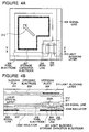
- Figure 4A there is shown an enlarged view of one pixel section on a main plate in another embodiment of the liquid crystal display apparatus in accordance with the present invention
- Figure 4B is a sectional view of the liquid crystal display apparatus taken along the line B-B in Figure 4A.
- elements similar or corresponding to those shown in Figures 3A and 3B are given Reference Numerals obtained by adding "100" to Reference Numerals given to the corresponding elements shown in Figures 3A and 3B. Therefore, a detailed explanation of the same elements as those shown in Figures 3A and 3B will be omitted.
- a scan line 202 and a signal line 203 formed of chromium, a TFT 205 formed of amorphous silicon, and a pixel electrode 206 formed of ITO were formed, and a storage capacitor electrode 207 formed of chromium acting as a light blocking layer was formed through an insulating layer 204.
- an opposing electrode 209 formed of ITO and a light blocking layer 210 formed of chromium were deposited.
- the light-blocking layer 210 has a configuration and size capable of covering the TFT 205 even if misalignment between the two plates becomes a maximum
- the storage capacitor electrode 207 has a configuration and size capable of ensuring that the light-blocking layer 210 never becomes visible within the pixel aperture even if misalignment between the two plates becomes a maximum.
- the storage capacitor electrode 207 has a portion overlapping with a periphery of the pixel electrode 206, and particularly, the width of the overlapping portion of the storage capacitor electrode 207 was widened in a special area determined on the basis of a rubbing direction.
- a polyimide aligning film 211 was coated on a surface of each of the plates, and then baked. A rubbing treatment was performed on the plates thus treated so that when the plates are coupled to each other, the orientation direction of each plate becomes substantially perpendicular to that of the other plate. Thereafter, the plates were coupled to each other in such a manner that a spacing of about 5 ⁇ m was formed between the plates, and a TN liquid crystal material 212 was injected into the spacing between the plates. Then, the plates were encapsulated. Thus, a liquid crystal display apparatus was obtained.
- an arrow 213 indicates the rubbing direction of the main plate.
- liquid crystal display apparatus thus obtained, a display was performed in the same conditions as those for the first embodiment.
- a pixel pitch of 65 ⁇ m a clear image having the aperture ratio of not less than 35% and the lightness/darkness ratio of not less than 200 : 1 could be easily realized.
- this liquid crystal display apparatus was incorporated into a projection type optical system so that an enlarged image is projected in magnification of about 25 times. In this case, an image having a sufficient bright and excellent visibility could be obtained.
- the light blocking layer 210 is provided on the opposing plate in order to prevent the switching device 205 from being exposed to light.
- the area of the light blocking layer 210 can be limited to a necessary minimum extent corresponding to the switching device 205.
- the light blocking storage capacitor electrode 207 determining the shape of the pixel aperture is provided on the main plate, similarly to the first embodiment, it is possible to perform at a high degree of precision alignment between the pixel electrode 206 and the light blocking storage capacitor electrode 207. Accordingly, it is not necessary to greatly narrow the pixel aperture.
- chromium was used as the electrode material for the scan line, the signal line and the storage capacitor electrode.
- the electrode material is in no way limited to chromium, and any material having a light blocking property and an electrical conductivity, for example, aluminum and molybdenum, can be used.
- the material for the pixel electrode and the opposing electrode is not limited to ITO, but any light transparent electrical conductive material can be used.
- the material for the switching device is not limited to the amorphous silicon, but other material such as a polycrystalline silicon can be used. These are a matter of course.
- the distortion of the signal waveform which would be caused by the capacitive coupling become no problem, if, in a liquid crystal panel having a diagonal size of not greater than 6 inches, the insulating layer is formed of a silicon oxide or silicon nitride thin film having the thickness not less than 3000 ⁇ .
- the distortion of the signal waveform can be suppressed to a not-problem level by using aluminum as a wiring material for the purpose of decreasing the wiring resistance.
- the present invention has been explained in connection with the display apparatus.
- the advantage of the present invention is not limited to the display apparatus, and the present invention can be advantageously applied to other devices utilizing a light modulation effect of the liquid crystal, for example, a printer head, or an image sensor.
- the present invention it becomes possible, in the liquid crystal device having the switching device, to suppress the orientation abnormality of the liquid crystal occurring at the periphery of the pixel electrode so as to prevent the light leakage at the boundary of the pixel, without narrowing the pixel aperture and with a high precision of alignment.
- This enables to realize a high quality display without decreasing the light utility efficiency in the liquid crystal device.
- this is effective in miniaturizing the liquid crystal display apparatus with a high density.
Landscapes
- Physics & Mathematics (AREA)
- Nonlinear Science (AREA)
- Engineering & Computer Science (AREA)
- Microelectronics & Electronic Packaging (AREA)
- Mathematical Physics (AREA)
- Chemical & Material Sciences (AREA)
- Crystallography & Structural Chemistry (AREA)
- General Physics & Mathematics (AREA)
- Optics & Photonics (AREA)
- Power Engineering (AREA)
- Liquid Crystal (AREA)
Applications Claiming Priority (4)
| Application Number | Priority Date | Filing Date | Title |
|---|---|---|---|
| JP292850/92 | 1992-10-30 | ||
| JP29285092 | 1992-10-30 | ||
| JP15176493A JPH06194687A (ja) | 1992-10-30 | 1993-06-23 | 透過型アクティブマトリクス型液晶素子 |
| JP151764/93 | 1993-06-23 |
Publications (2)
| Publication Number | Publication Date |
|---|---|
| EP0595363A1 true EP0595363A1 (fr) | 1994-05-04 |
| EP0595363B1 EP0595363B1 (fr) | 1998-02-11 |
Family
ID=26480898
Family Applications (1)
| Application Number | Title | Priority Date | Filing Date |
|---|---|---|---|
| EP93117683A Expired - Lifetime EP0595363B1 (fr) | 1992-10-30 | 1993-11-02 | Dispositif à cristal liquide à matrice active du type à transmission |
Country Status (5)
| Country | Link |
|---|---|
| US (1) | US5510916A (fr) |
| EP (1) | EP0595363B1 (fr) |
| JP (1) | JPH06194687A (fr) |
| KR (1) | KR0150806B1 (fr) |
| DE (1) | DE69316957T2 (fr) |
Cited By (4)
| Publication number | Priority date | Publication date | Assignee | Title |
|---|---|---|---|---|
| GB2307326A (en) * | 1995-11-20 | 1997-05-21 | Hyundai Electronics Ind | Liquid crystal display |
| DE19650787C2 (de) * | 1995-12-08 | 2000-04-13 | Lg Semicon Co Ltd | Flüssigkristall-Anzeigevorrichtung mit Dünnfilmtransistor und Verfahren zum Herstellen derselben |
| WO2006093029A1 (fr) * | 2005-02-28 | 2006-09-08 | Casio Computer Co., Ltd. | Panneau tft |
| US7795621B2 (en) | 2005-02-28 | 2010-09-14 | Casio Computer Co., Ltd. | Thin film transistor panel |
Families Citing this family (72)
| Publication number | Priority date | Publication date | Assignee | Title |
|---|---|---|---|---|
| US5682211A (en) * | 1994-04-28 | 1997-10-28 | Xerox Corporation | Integrated dark matrix for an active matrix liquid crystal display with pixel electrodes overlapping gate data lines |
| JP2934875B2 (ja) * | 1994-09-30 | 1999-08-16 | カシオ計算機株式会社 | マトリックス型液晶表示装置 |
| US5710611A (en) * | 1994-11-17 | 1998-01-20 | Nec Corporation | Liquid crystal display apparatus preventing image on screen from influences of disclination line |
| FR2731526B1 (fr) * | 1995-03-09 | 1997-04-04 | Thomson Consumer Electronics | Ecran a cristaux liquides a angle de vue ameliore |
| KR100303134B1 (ko) * | 1995-05-09 | 2002-11-23 | 엘지.필립스 엘시디 주식회사 | 액정표시소자및그제조방법. |
| US5666174A (en) * | 1995-08-11 | 1997-09-09 | Cupolo, Iii; Anthony M. | Emissive liquid crystal display with liquid crystal between radiation source and phosphor layer |
| JPH09113922A (ja) * | 1995-10-03 | 1997-05-02 | Internatl Business Mach Corp <Ibm> | 液晶表示装置及びその製造方法 |
| US5782665A (en) * | 1995-12-29 | 1998-07-21 | Xerox Corporation | Fabricating array with storage capacitor between cell electrode and dark matrix |
| KR970062775A (ko) * | 1996-02-03 | 1997-09-12 | 구자홍 | 액정표시소자의 블랙매트릭스 및 그 제조방법 |
| JPH09281508A (ja) * | 1996-04-12 | 1997-10-31 | Semiconductor Energy Lab Co Ltd | 液晶表示装置およびその作製方法 |
| US6038006A (en) * | 1996-09-02 | 2000-03-14 | Casio Computer Co., Ltd. | Liquid crystal display device with light shield and color filter overlapping two edges of pixel electrode |
| JPH10115840A (ja) * | 1996-10-08 | 1998-05-06 | Casio Comput Co Ltd | マトリックス型液晶表示装置 |
| US5879959A (en) * | 1997-01-17 | 1999-03-09 | Industrial Technology Research Institute | Thin-film transistor structure for liquid crystal display |
| US6088070A (en) * | 1997-01-17 | 2000-07-11 | Semiconductor Energy Laboratory Co., Ltd. | Active matrix liquid crystal with capacitor between light blocking film and pixel connecting electrode |
| JP3784491B2 (ja) | 1997-03-28 | 2006-06-14 | 株式会社半導体エネルギー研究所 | アクティブマトリクス型の表示装置 |
| JP3935246B2 (ja) | 1997-08-18 | 2007-06-20 | エルジー フィリップス エルシーディー カンパニー リミテッド | 液晶表示装置 |
| US6624860B1 (en) * | 1998-01-26 | 2003-09-23 | Sharp Kabushiki Kaisha | Color filter layer providing transmitted light with improved brightness and display device using same |
| US6215538B1 (en) * | 1998-01-26 | 2001-04-10 | Sharp Kabushiki Kaisha | Liquid crystal display including both color filter and non-color filter regions for increasing brightness |
| JP4312851B2 (ja) * | 1998-04-27 | 2009-08-12 | 株式会社半導体エネルギー研究所 | 半導体装置およびその作製方法 |
| KR100313949B1 (ko) * | 1998-11-11 | 2002-09-17 | 엘지.필립스 엘시디 주식회사 | 멀티도메인액정표시소자 |
| US6900869B1 (en) | 1998-11-25 | 2005-05-31 | Lg. Philips Lcd Co., Ltd. | Multi-domain liquid crystal display device with particular dielectric structures |
| JP4362882B2 (ja) * | 1999-01-13 | 2009-11-11 | ソニー株式会社 | 液晶パネル、液晶パネルの製造方法および液晶表示装置 |
| US7202924B1 (en) | 1999-03-17 | 2007-04-10 | Lg.Philips Lcd Co., Ltd | Liquid crystal display and a fabricating method thereof |
| US6445003B1 (en) * | 1999-05-11 | 2002-09-03 | Lg.Philips Lcd Co., Ltd. | Thin film transistor (TFT) type optical detecting sensor |
| JP3889533B2 (ja) * | 1999-09-22 | 2007-03-07 | シャープ株式会社 | 液晶表示装置及びその製造方法 |
| JP3374911B2 (ja) * | 1999-09-30 | 2003-02-10 | 日本電気株式会社 | 透過液晶パネル、画像表示装置、パネル製造方法 |
| US6906768B1 (en) | 1999-11-24 | 2005-06-14 | Lg.Philips Lcd Co., Ltd. | Multi-domain liquid crystal display device with particular dielectric structures |
| US6590227B2 (en) * | 1999-12-27 | 2003-07-08 | Semiconductor Energy Laboratory Co., Ltd. | Active matrix display device |
| KR20010060518A (ko) * | 1999-12-27 | 2001-07-07 | 윤종용 | 액정 표시 장치 |
| TWI301915B (fr) * | 2000-03-17 | 2008-10-11 | Seiko Epson Corp | |
| KR100695299B1 (ko) * | 2000-05-12 | 2007-03-14 | 삼성전자주식회사 | 액정 표시 장치용 박막 트랜지스터 기판 및 그의 제조 방법 |
| KR100623989B1 (ko) * | 2000-05-23 | 2006-09-13 | 삼성전자주식회사 | 액정 표시 장치용 박막 트랜지스터 기판 및 그의 수리 방법 |
| JP3792485B2 (ja) * | 2000-06-02 | 2006-07-05 | Nec液晶テクノロジー株式会社 | アクティブマトリクス型液晶表示装置 |
| JP3460706B2 (ja) * | 2000-08-07 | 2003-10-27 | セイコーエプソン株式会社 | 電気光学装置、電子機器、電気光学装置用基板および電気光学装置用基板の製造方法。 |
| JP4212791B2 (ja) * | 2000-08-09 | 2009-01-21 | シャープ株式会社 | 液晶表示装置ならびに携帯電子機器 |
| US6767609B2 (en) * | 2000-09-15 | 2004-07-27 | 3M Innovative Properties Company | Perforated film constructions for backlit signs |
| JP4368096B2 (ja) * | 2001-10-02 | 2009-11-18 | シャープ株式会社 | 液晶表示装置 |
| JP4050119B2 (ja) * | 2001-10-02 | 2008-02-20 | シャープ株式会社 | 液晶表示装置 |
| US7053967B2 (en) | 2002-05-23 | 2006-05-30 | Planar Systems, Inc. | Light sensitive display |
| US7009663B2 (en) * | 2003-12-17 | 2006-03-07 | Planar Systems, Inc. | Integrated optical light sensitive active matrix liquid crystal display |
| WO2003073159A1 (fr) * | 2002-02-20 | 2003-09-04 | Planar Systems, Inc. | Ecran photosensible |
| WO2003075207A2 (fr) * | 2002-03-01 | 2003-09-12 | Planar Systems, Inc. | Ecrans tactiles antireflets |
| TWI261135B (en) * | 2002-05-28 | 2006-09-01 | Chi Mei Optoelectronics Corp | Method for fabricating thin film transistors of a TFT-LCD |
| US20080084374A1 (en) * | 2003-02-20 | 2008-04-10 | Planar Systems, Inc. | Light sensitive display |
| US20080048995A1 (en) * | 2003-02-20 | 2008-02-28 | Planar Systems, Inc. | Light sensitive display |
| US20050134749A1 (en) * | 2003-12-19 | 2005-06-23 | Adiel Abileah | Reflection resistant display |
| JP3841095B2 (ja) * | 2004-01-23 | 2006-11-01 | セイコーエプソン株式会社 | 液晶装置および投射型表示装置 |
| JP2005241910A (ja) * | 2004-02-26 | 2005-09-08 | Nec Corp | 薄膜トランジスタアレイ基板、それを用いた液晶パネルおよび液晶プロジェクタ |
| US7773139B2 (en) * | 2004-04-16 | 2010-08-10 | Apple Inc. | Image sensor with photosensitive thin film transistors |
| US20060045240A1 (en) * | 2004-08-31 | 2006-03-02 | Buchner Gregory C | Method and apparatus for delayed answering of telecommunications request |
| US20070109239A1 (en) * | 2005-11-14 | 2007-05-17 | Den Boer Willem | Integrated light sensitive liquid crystal display |
| JP2007212499A (ja) * | 2006-02-07 | 2007-08-23 | Seiko Epson Corp | 液晶装置及びプロジェクタ |
| US8101442B2 (en) * | 2008-03-05 | 2012-01-24 | Semiconductor Energy Laboratory Co., Ltd. | Method for manufacturing EL display device |
| US7989275B2 (en) * | 2008-03-10 | 2011-08-02 | Semiconductor Energy Laboratory Co., Ltd. | Thin film transistor, manufacturing method thereof, display device, and manufacturing method thereof |
| US8681279B2 (en) * | 2009-10-29 | 2014-03-25 | Sharp Kabushiki Kaisha | Optical sensor, semiconductor device, and liquid crystal panel |
| US9310923B2 (en) | 2010-12-03 | 2016-04-12 | Apple Inc. | Input device for touch sensitive devices |
| US9329703B2 (en) | 2011-06-22 | 2016-05-03 | Apple Inc. | Intelligent stylus |
| US8638320B2 (en) | 2011-06-22 | 2014-01-28 | Apple Inc. | Stylus orientation detection |
| US8928635B2 (en) | 2011-06-22 | 2015-01-06 | Apple Inc. | Active stylus |
| CN103529589B (zh) * | 2012-07-05 | 2016-12-28 | 乐金显示有限公司 | 立体图像显示器及其制造方法 |
| US9652090B2 (en) | 2012-07-27 | 2017-05-16 | Apple Inc. | Device for digital communication through capacitive coupling |
| US9557845B2 (en) | 2012-07-27 | 2017-01-31 | Apple Inc. | Input device for and method of communication with capacitive devices through frequency variation |
| US9176604B2 (en) | 2012-07-27 | 2015-11-03 | Apple Inc. | Stylus device |
| US10048775B2 (en) | 2013-03-14 | 2018-08-14 | Apple Inc. | Stylus detection and demodulation |
| US10845901B2 (en) | 2013-07-31 | 2020-11-24 | Apple Inc. | Touch controller architecture |
| CN103941505B (zh) | 2014-03-06 | 2017-03-15 | 京东方科技集团股份有限公司 | 一种阵列基板及其制备方法和显示装置 |
| US10061450B2 (en) | 2014-12-04 | 2018-08-28 | Apple Inc. | Coarse scan and targeted active mode scan for touch |
| CN104880879A (zh) | 2015-06-19 | 2015-09-02 | 京东方科技集团股份有限公司 | Coa阵列基板及其制造方法、显示装置 |
| CN105446000B (zh) * | 2016-01-21 | 2018-07-10 | 武汉华星光电技术有限公司 | 护眼式液晶显示装置的制作方法 |
| US10474277B2 (en) | 2016-05-31 | 2019-11-12 | Apple Inc. | Position-based stylus communication |
| KR102819878B1 (ko) | 2019-03-15 | 2025-06-12 | 삼성디스플레이 주식회사 | 표시 장치 |
| US12153764B1 (en) | 2020-09-25 | 2024-11-26 | Apple Inc. | Stylus with receive architecture for position determination |
Citations (5)
| Publication number | Priority date | Publication date | Assignee | Title |
|---|---|---|---|---|
| EP0136509A2 (fr) * | 1983-08-23 | 1985-04-10 | Kabushiki Kaisha Toshiba | Dispositif d'affichage actif du type à matrice |
| JPS60207116A (ja) * | 1984-03-31 | 1985-10-18 | Toshiba Corp | 表示電極アレイ |
| US4733948A (en) * | 1984-12-20 | 1988-03-29 | Canon Kabushiki Kaisha | Color liquid crystal display with light intercepting member |
| JPH04331924A (ja) * | 1991-05-07 | 1992-11-19 | Sanyo Electric Co Ltd | 液晶表示装置 |
| EP0524067A1 (fr) * | 1991-07-11 | 1993-01-20 | France Telecom | Structure d'écran à cristal liquide, à matrice active et à haute définition |
Family Cites Families (9)
| Publication number | Priority date | Publication date | Assignee | Title |
|---|---|---|---|---|
| JPS60120321A (ja) * | 1983-12-02 | 1985-06-27 | Matsushita Electric Ind Co Ltd | カラ−液晶表示装置 |
| JPS60133493A (ja) * | 1983-12-21 | 1985-07-16 | 三菱電機株式会社 | マトリツクス型液晶表示装置 |
| JPS6211829A (ja) * | 1985-03-28 | 1987-01-20 | Toshiba Corp | アクテイブマトリツクス形液晶表示装置 |
| JP2828990B2 (ja) * | 1988-04-19 | 1998-11-25 | 株式会社東芝 | 液晶表示素子 |
| JPH0213927A (ja) * | 1988-07-01 | 1990-01-18 | Hitachi Ltd | 液晶表示パネル |
| JP2693513B2 (ja) * | 1988-08-30 | 1997-12-24 | 株式会社東芝 | アクティブマトリクス型液晶表示素子 |
| JPH03125123A (ja) * | 1989-10-09 | 1991-05-28 | Sharp Corp | アクティブマトリクス表示装置及びその製造方法 |
| JPH03239229A (ja) * | 1990-02-16 | 1991-10-24 | Sharp Corp | アクティブマトリクス液晶表示装置 |
| KR940004322B1 (ko) * | 1991-09-05 | 1994-05-19 | 삼성전자 주식회사 | 액정표시장치 및 그 제조방법 |
-
1993
- 1993-06-23 JP JP15176493A patent/JPH06194687A/ja active Pending
- 1993-10-30 KR KR1019930022852A patent/KR0150806B1/ko not_active Expired - Lifetime
- 1993-11-01 US US08/143,738 patent/US5510916A/en not_active Expired - Lifetime
- 1993-11-02 DE DE69316957T patent/DE69316957T2/de not_active Expired - Lifetime
- 1993-11-02 EP EP93117683A patent/EP0595363B1/fr not_active Expired - Lifetime
Patent Citations (5)
| Publication number | Priority date | Publication date | Assignee | Title |
|---|---|---|---|---|
| EP0136509A2 (fr) * | 1983-08-23 | 1985-04-10 | Kabushiki Kaisha Toshiba | Dispositif d'affichage actif du type à matrice |
| JPS60207116A (ja) * | 1984-03-31 | 1985-10-18 | Toshiba Corp | 表示電極アレイ |
| US4733948A (en) * | 1984-12-20 | 1988-03-29 | Canon Kabushiki Kaisha | Color liquid crystal display with light intercepting member |
| JPH04331924A (ja) * | 1991-05-07 | 1992-11-19 | Sanyo Electric Co Ltd | 液晶表示装置 |
| EP0524067A1 (fr) * | 1991-07-11 | 1993-01-20 | France Telecom | Structure d'écran à cristal liquide, à matrice active et à haute définition |
Non-Patent Citations (3)
| Title |
|---|
| M. TSUMURA ET AL.: "High-Resolution 10.3-in. Diagonal Multicolor TFT-LCD", SID INTERNATIONAL SYMPOSIUM - DIGEST OF TECHNICAL PAPERS., 1991, PLAYA DEL REY, US, pages 215 - 218 * |
| PATENT ABSTRACTS OF JAPAN vol. 010, no. 068 (P - 437) 18 March 1986 (1986-03-18) * |
| PATENT ABSTRACTS OF JAPAN vol. 017, no. 175 (P - 1516) 5 April 1993 (1993-04-05) * |
Cited By (7)
| Publication number | Priority date | Publication date | Assignee | Title |
|---|---|---|---|---|
| GB2307326A (en) * | 1995-11-20 | 1997-05-21 | Hyundai Electronics Ind | Liquid crystal display |
| US5929501A (en) * | 1995-11-20 | 1999-07-27 | Hyundai Electronics Industries Co., Ltd. | Liquid crystal display device with storage capacitor and method of fabricating |
| GB2307326B (en) * | 1995-11-20 | 2000-03-08 | Hyundai Electronics Ind | Liquid crystal display device and method of fabricating the same |
| DE19650787C2 (de) * | 1995-12-08 | 2000-04-13 | Lg Semicon Co Ltd | Flüssigkristall-Anzeigevorrichtung mit Dünnfilmtransistor und Verfahren zum Herstellen derselben |
| WO2006093029A1 (fr) * | 2005-02-28 | 2006-09-08 | Casio Computer Co., Ltd. | Panneau tft |
| US7633090B2 (en) | 2005-02-28 | 2009-12-15 | Casio Computer Co., Ltd. | Thin film transistor panel |
| US7795621B2 (en) | 2005-02-28 | 2010-09-14 | Casio Computer Co., Ltd. | Thin film transistor panel |
Also Published As
| Publication number | Publication date |
|---|---|
| DE69316957T2 (de) | 1998-07-30 |
| JPH06194687A (ja) | 1994-07-15 |
| DE69316957D1 (de) | 1998-03-19 |
| EP0595363B1 (fr) | 1998-02-11 |
| US5510916A (en) | 1996-04-23 |
| KR0150806B1 (ko) | 1998-10-15 |
Similar Documents
| Publication | Publication Date | Title |
|---|---|---|
| US5510916A (en) | Active matrix liquid crystal device with opposite substrate having black matrix with larger aperture than active substrate | |
| US7342621B2 (en) | Thin film transistor substrate for a liquid crystal display wherein a black matrix formed on the substrate comprises an inner aperture formed completely within the black matrix | |
| US5852485A (en) | Liquid crystal display device and method for producing the same | |
| KR100255584B1 (ko) | 액티브매트릭스형 액정표시장치 및 그 제조방법 | |
| KR100713188B1 (ko) | 액티브매트릭스 액정표시장치 | |
| KR100250093B1 (ko) | 액티브 매트릭스 기판 및 그 제조 방법 | |
| KR100291228B1 (ko) | 액정패널 | |
| KR101112537B1 (ko) | 다중 도메인 액정 표시 장치 및 그에 사용되는 표시판 | |
| JP3378820B2 (ja) | 垂直配向型液晶表示装置 | |
| KR100413577B1 (ko) | 액티브 매트릭스 액정 표시 장치 | |
| KR100832202B1 (ko) | 액정 표시 장치용 기판 및 그것을 구비한 액정 표시 장치 | |
| KR100266434B1 (ko) | 액티브매트릭스액정패널및그것을사용하는프로젝션시스템 | |
| KR100920348B1 (ko) | 액정 표시 장치 | |
| KR101122618B1 (ko) | 액정 표시 장치 및 이를 위한 스토리지 커패시터 | |
| US20060092360A1 (en) | Multi-domain liquid crystal display device and fabrication method thereof | |
| JP3864036B2 (ja) | 液晶表示装置 | |
| KR100590932B1 (ko) | 프린지 필드 스위칭 모드 액정표시장치 | |
| US7233376B2 (en) | Transflective LCD with reflective electrode offset from transmissile electrode | |
| JP2858499B2 (ja) | 液晶素子の駆動方法 | |
| US20030142254A1 (en) | Reflective liquid crystal display and method for fabricating the same | |
| JPH0980473A (ja) | 液晶表示素子 | |
| JP3583534B2 (ja) | アクティブマトリックス型液晶表示パネル | |
| KR100983577B1 (ko) | 액정표시소자 | |
| JP3312720B2 (ja) | 液晶表示装置 | |
| US7050136B2 (en) | Array substrate for use in in-plane switching mode liquid crystal display device |
Legal Events
| Date | Code | Title | Description |
|---|---|---|---|
| PUAI | Public reference made under article 153(3) epc to a published international application that has entered the european phase |
Free format text: ORIGINAL CODE: 0009012 |
|
| 17P | Request for examination filed |
Effective date: 19940225 |
|
| AK | Designated contracting states |
Kind code of ref document: A1 Designated state(s): DE FR GB IT NL |
|
| 17Q | First examination report despatched |
Effective date: 19960130 |
|
| GRAG | Despatch of communication of intention to grant |
Free format text: ORIGINAL CODE: EPIDOS AGRA |
|
| GRAG | Despatch of communication of intention to grant |
Free format text: ORIGINAL CODE: EPIDOS AGRA |
|
| GRAH | Despatch of communication of intention to grant a patent |
Free format text: ORIGINAL CODE: EPIDOS IGRA |
|
| GRAH | Despatch of communication of intention to grant a patent |
Free format text: ORIGINAL CODE: EPIDOS IGRA |
|
| GRAA | (expected) grant |
Free format text: ORIGINAL CODE: 0009210 |
|
| AK | Designated contracting states |
Kind code of ref document: B1 Designated state(s): DE FR GB IT NL |
|
| REF | Corresponds to: |
Ref document number: 69316957 Country of ref document: DE Date of ref document: 19980319 |
|
| ITF | It: translation for a ep patent filed | ||
| ET | Fr: translation filed | ||
| PLBE | No opposition filed within time limit |
Free format text: ORIGINAL CODE: 0009261 |
|
| STAA | Information on the status of an ep patent application or granted ep patent |
Free format text: STATUS: NO OPPOSITION FILED WITHIN TIME LIMIT |
|
| 26N | No opposition filed | ||
| REG | Reference to a national code |
Ref country code: GB Ref legal event code: IF02 |
|
| PGFP | Annual fee paid to national office [announced via postgrant information from national office to epo] |
Ref country code: FR Payment date: 20121130 Year of fee payment: 20 Ref country code: DE Payment date: 20121031 Year of fee payment: 20 |
|
| REG | Reference to a national code |
Ref country code: DE Ref legal event code: R082 Ref document number: 69316957 Country of ref document: DE Ref country code: DE Ref legal event code: R082 Ref document number: 69316957 Country of ref document: DE Representative=s name: MURGITROYD & COMPANY, DE |
|
| PGFP | Annual fee paid to national office [announced via postgrant information from national office to epo] |
Ref country code: GB Payment date: 20121031 Year of fee payment: 20 Ref country code: IT Payment date: 20121110 Year of fee payment: 20 |
|
| REG | Reference to a national code |
Ref country code: FR Ref legal event code: TP Owner name: GOLD CHARM LIMITED, JP Effective date: 20130211 |
|
| PGFP | Annual fee paid to national office [announced via postgrant information from national office to epo] |
Ref country code: NL Payment date: 20121116 Year of fee payment: 20 |
|
| REG | Reference to a national code |
Ref country code: NL Ref legal event code: SD Effective date: 20130329 |
|
| REG | Reference to a national code |
Ref country code: DE Ref legal event code: R082 Ref document number: 69316957 Country of ref document: DE Representative=s name: MURGITROYD & COMPANY, DE Effective date: 20130321 Ref country code: DE Ref legal event code: R082 Ref document number: 69316957 Country of ref document: DE Representative=s name: MURGITROYD & COMPANY, DE Effective date: 20130211 Ref country code: DE Ref legal event code: R081 Ref document number: 69316957 Country of ref document: DE Owner name: GOLD CHARM LIMITED, WS Free format text: FORMER OWNER: NEC CORP., TOKYO, JP Effective date: 20130305 |
|
| REG | Reference to a national code |
Ref country code: DE Ref legal event code: R071 Ref document number: 69316957 Country of ref document: DE |
|
| REG | Reference to a national code |
Ref country code: NL Ref legal event code: V4 Effective date: 20131102 |
|
| REG | Reference to a national code |
Ref country code: GB Ref legal event code: PE20 Expiry date: 20131101 |
|
| PG25 | Lapsed in a contracting state [announced via postgrant information from national office to epo] |
Ref country code: GB Free format text: LAPSE BECAUSE OF EXPIRATION OF PROTECTION Effective date: 20131101 Ref country code: DE Free format text: LAPSE BECAUSE OF EXPIRATION OF PROTECTION Effective date: 20131105 |