EP0595748A1 - Schaltungen zur Detektion des Einschaltens - Google Patents
Schaltungen zur Detektion des Einschaltens Download PDFInfo
- Publication number
- EP0595748A1 EP0595748A1 EP93480138A EP93480138A EP0595748A1 EP 0595748 A1 EP0595748 A1 EP 0595748A1 EP 93480138 A EP93480138 A EP 93480138A EP 93480138 A EP93480138 A EP 93480138A EP 0595748 A1 EP0595748 A1 EP 0595748A1
- Authority
- EP
- European Patent Office
- Prior art keywords
- power
- transistor
- circuit
- detection circuit
- set forth
- Prior art date
- Legal status (The legal status is an assumption and is not a legal conclusion. Google has not performed a legal analysis and makes no representation as to the accuracy of the status listed.)
- Withdrawn
Links
- 238000001514 detection method Methods 0.000 title claims abstract description 37
- 239000003990 capacitor Substances 0.000 claims abstract description 19
- 230000008878 coupling Effects 0.000 claims abstract description 3
- 238000010168 coupling process Methods 0.000 claims abstract description 3
- 238000005859 coupling reaction Methods 0.000 claims abstract description 3
- 230000005669 field effect Effects 0.000 claims description 30
- 238000000034 method Methods 0.000 description 9
- 230000008569 process Effects 0.000 description 9
- 230000007704 transition Effects 0.000 description 8
- 238000010586 diagram Methods 0.000 description 5
- 239000004065 semiconductor Substances 0.000 description 5
- 238000007792 addition Methods 0.000 description 4
- 238000005516 engineering process Methods 0.000 description 4
- 230000004048 modification Effects 0.000 description 4
- 238000012986 modification Methods 0.000 description 4
- 230000003111 delayed effect Effects 0.000 description 3
- 230000008859 change Effects 0.000 description 2
- 230000001276 controlling effect Effects 0.000 description 2
- 230000007423 decrease Effects 0.000 description 2
- 238000013461 design Methods 0.000 description 2
- 238000007599 discharging Methods 0.000 description 2
- 230000010355 oscillation Effects 0.000 description 2
- 230000001105 regulatory effect Effects 0.000 description 2
- 230000004044 response Effects 0.000 description 2
- 238000004088 simulation Methods 0.000 description 2
- 239000000758 substrate Substances 0.000 description 2
- 230000002411 adverse Effects 0.000 description 1
- 230000000295 complement effect Effects 0.000 description 1
- 230000001419 dependent effect Effects 0.000 description 1
- 230000000694 effects Effects 0.000 description 1
- 230000008030 elimination Effects 0.000 description 1
- 238000003379 elimination reaction Methods 0.000 description 1
- 230000007613 environmental effect Effects 0.000 description 1
- 230000010354 integration Effects 0.000 description 1
- 229910044991 metal oxide Inorganic materials 0.000 description 1
- 150000004706 metal oxides Chemical class 0.000 description 1
- 238000005457 optimization Methods 0.000 description 1
- 238000012856 packing Methods 0.000 description 1
- 230000000704 physical effect Effects 0.000 description 1
- 230000000630 rising effect Effects 0.000 description 1
- 230000035945 sensitivity Effects 0.000 description 1
- 238000012360 testing method Methods 0.000 description 1
- 230000001052 transient effect Effects 0.000 description 1
Images



Classifications
-
- H—ELECTRICITY
- H03—ELECTRONIC CIRCUITRY
- H03K—PULSE TECHNIQUE
- H03K17/00—Electronic switching or gating, i.e. not by contact-making and –breaking
- H03K17/22—Modifications for ensuring a predetermined initial state when the supply voltage has been applied
- H03K17/223—Modifications for ensuring a predetermined initial state when the supply voltage has been applied in field-effect transistor switches
Definitions
- This invention relates to power up detection circuits, which are also known as power on reset circuits, for reliable high density integrated circuit operation.
- a reliable power on reset pulse greatly simplifies and improves the reliability of circuit designs for, e.g., enabling redundancy, maintaining off chip drivers in a tri-state condition during power up and controlling clock logic so that the integrated circuit does not power up into an undesirable mode.
- a reset signal generating circuit which includes a first switch controlled by a divided voltage from a voltage dividing circuit turned on when the power source voltage rises to a value in the vicinity of a predetermined value with an arbitrary rising speed and a second switch turned on by the first switch and connected to a capacitor for charging and discharging the capacitor to provide a reset signal.
- a power-up reset circuit which includes first and second serially connected field effect transistors disposed between a power supply voltage and an input of an inverter, a capacitor connected between the input of the inverter and the low supply voltage, with current flowing through the field effect transistors to charge the capacitor only when the supply voltage is greater than the sum of the absolute values of their threshold voltages and a depletion mode transistor shunting to ground any subthreshold leakage through the first and second transistors.
- U.S. Patent 5,030,845 by A.M. Love et al, issued July 9, 1991, discloses a power-up pulse generator circuit in which channel width-to-length ratios of transistors are used to control a subthreshold current during the initial part of the power-up transient.
- Prior art for power up detect circuits generally features components connected to an effective RC delay circuit.
- the delayed mode is then compared to, e.g., the power supply to determine that sufficient voltage has been applied to the integrated circuit chip for proper circuit operation.
- This type of power up detect circuit may operate satisfactorily in applications where power supply ramp rates are relatively fast, such as in circuit testers and personal computers, but it becomes less reliable in larger systems where ramp rates are several hundred milli-seconds.
- Effective power up detect circuits must be able to function reliably in systems having very fast to very slow power supply ramp rates.
- a power on reset circuit which includes an output terminal connected through an impedance to a power supply, with the output being further connected through a subthreshold leakage device of a latch to a point of reference potential, the subthreshold leakage device being switched from an initial subthreshold mode to a conduction mode in response to a predetermined level of output voltage developed on the output terminal.
- FIG. 1 a circuit diagram of one embodiment of the power up detection or reset circuit of the present invention which is made on a semiconductor substrate or integrated circuit chip preferably in the complementary metal oxide semiconductor, CMOS, technology.
- the circuit of FIG. 1 of the drawings includes a first P-channel field effect transistor P0 and a serially connected first N-channel field effect transistor N0 connected between a power supply Vdd of, e.g., 3.6 volts, and a power on detect output terminal POD, with the drain electrodes of the transistors P0 and N0 being interconnected at a common point and a gate electrode of the transistor N0 being connected to the common point and the gate electrode of the transistor PO being connected to a point of reference potential such as ground.
- Vdd voltage supply
- POD power on detect output terminal
- a latch L has a first inverter I0 and a second inverter I1, with the first inverter I0 having a second P-channel field effect transistor P1 and a serially connected N-channel field effect transistor N1 disposed between the power supply Vdd and the point of reference potential or ground and the second inverter 11 having a third P-channel field effect transistor P2 and a serially connected N-channel field effect transistor N2 also disposed between the power supply Vdd and ground.
- Drain electrodes of the second P-channel and second N-channel transistors P1 and N1 are connected to the output terminal POD and gate electrodes of each of the third P-channel and third N-channel transistors P2 and N2 are connected to the output terminal POD, with the drains of the third P-channel and third N-channel transistors P2 and N2 being connected to each of the gate electrodes of the second P-channel and second N-channel transistors P1 and N1.
- a linear non-voltage dependent capacitor C is connected between the power supply Vdd and the drains of the third P-channel and third N-channel transistors P2 and N2.
- the physical property of field effect transistors controlling the subthreshold current is used.
- This subthreshold current occurs in what is normally called the OFF state of the field effect transistor, i.e., prior to the time that the transistor has its threshold voltage applied to its gate electrode.
- the subthreshold current has a value in the 1 picoampere to the 100 nanoampere range.
- a characteristic of the subthreshold current is that it varies with the transistor or device length in short devices, however, this variability decreases for long devices. Therefore, by utilizing subthreshold currents of various length devices connected in the latch L, as illustrated in FIG.
- latch L is very significant in that it provides a rapid change of state during slow power supply ramp up in order to avoid oscillations in the circuit it is intended to initialize. Slow state transitions affect logic circuits in much the same manner as indeterminate input levels.
- An example of desirable dimensions in micrometers of the width to length ratio, w/l, for the transistors of FIG. 1 is as follows: P0 is 20/0.80, N0 is 20/0.70, P1 is 4.5/1.0, N1 is 1.0/0.65, P2 is 4.5/0.75 and N2 is 1.5/0.9.
- the capacitor C in FIG. 1 (having a value of e.g. 0.35 picofarads) is added, preferably by utilizing the gate-to-source and gate-to-drain overlap capacitances of the PFET.
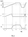
- each of the nodes POD, B and Vdd is at zero volts at time t0, as indicated in the graph of FIG. 2 of the drawings, with the voltage at the terminal Vdd of the power supply beginning to rise at time t1.
- subthreshold currents which may be from 1 to 100 picoamperes, begin to pass through the transistors P0, N0, P1, N1, P2 and N2.
- the subthreshold current passing through P-channel transistor P2 of the second inverter I1 charges node B to approximately the same voltage as Vdd, consequently, the capacitor C is not electrically active since the voltages on both plates of the capacitor rise at substantially the same rate.
- the rise in voltage of node B toward Vdd is due to the dimensions of the transistors P0, N0, P1, N1, P2 and N2, with the subthreshold current passing through the drain of the third P-channel transistor P2 being much greater than the subthreshold current passing through the drain of the third N-channel transistor N2. This difference in subthreshold current may be seen more clearly by referring to the graph of FIG.
- the dimensions of the second N-channel transistor N1 are such that the subthreshold current passing through its drain is much greater than the effective subthreshold current passing through the serially arranged first P-channel transistor P0 and first N-channel transistor N0 and through the drain of the second P-channel transistor P1.
- the initial state of the latch L has been set by the subthreshold currents.
- V TP of, e.g., 0.6 volt
- the transistors N1 and P2 of the latch L pass from the subthreshold conduction mode to the conduction or ON state.
- transistors P1 and N2 are still in the subthreshold mode at this time.
- the output terminal POD is still clamped to ground by the second N-channel transistor N1 being ON.
- the first P-channel transistor P0 is in the on state, and the first N-channel transistor N0 now passes from the subthreshold conduction mode to the ON state and supplies sufficient current to the output terminal POD that the second N-channel transistor N1 can no longer maintain the output terminal POD at ground.
- the overdrive on the third P-channel transistor P2 decreases and the third N-channel transistor N2 begins to turn on, discharging node B, as indicated in the graph of FIG. 2 at time t4. While the voltage on node B drops, the overdrive on the second N-channel transistor N1 is reduced allowing the voltage at the output terminal POD to rise further.
- the latch L rapidly changes state at approximately time t5, as indicated in the graph of FIG. 2 of the drawings.
- the second P-channel transistor P1 then continues to charge the output terminal POD toward a full Vdd voltage at time t6 while the third N-channel transistor N2 holds node B at ground, which insures the elimination of DC currents that could result if the circuit nodes were not fully charged or discharged to the terminal voltages of the power supply.
- the beta or width/length ratios of the latch L transistors P1, N1, P2 and N2 in relation to the first P-channel transistor P0 and first N-channel transistor N0 are defined such that the detected value of the voltage at the terminal Vdd is high enough to insure proper on chip logic circuit initialization for variable process parameters and temperatures.
- the capacitor C is now electrically active in the circuit.
- the capacitor C is used to insure that the voltage at node B continues to rise until the transistors P1, N1, P2 and N2 of the latch L are in the ON state.
- the second N-channel transistor N1 and the third P-channel transistor P2 control the voltage at the output terminal POD and at the node B as for the slow voltage ramp rate.
- the first P-channel transistor P0 and the first N-channel transistor N0 effect the changing of the state of the latch L at the appropriate value of the power supply voltage as indicated hereinabove in connection with the discussion of the operation of the circuit during the slow voltage ramp rate.
- this power up detection circuit may be used during a hot plug operation, i.e., during a fast voltage ramp down followed shortly thereafter with a ramp up, which occurs when a component or component card is plugged or unplugged while system power is still on.
- a power up detect circuit should operate properly for such an inadvertent occurrence.
- a hot plug incident appears as a rapid ramp down followed by a ramp up of the Vdd voltage.
- the voltage at the output terminal POD is at a full Vdd or 3.6 volts and the node B is at ground, as indicated in the graph of FIG. 2 at time t7.
- the voltage at the output terminal POD is discharged through the second P-channel transistor P1 to approximately 0.2 volts in about 50 nanoseconds. Due to the capacitor C, the voltage at node B is maintained between 0 and -0.5 volts which insures that the voltage at the output terminal POD reaches a low enough value at time t8 for a fast ramp up to proceed properly at time t9 of FIG. 2.
- the time for the fast ramp up is approximately 50 nanoseconds with the time between the completion of the fast ramp down at time t8 and the beginning of the fast ramp up at time t9 being approximately 50 nanoseconds.
- both the supply voltage Vdd and the output terminal voltage POD are at full power supply voltage of 3.6 volts.
- FIG. 4 is a circuit diagram, partly in block form, illustrating the power up detection circuit of the present invention when used to provide various desired and reliable output pulses even at very slow ramp speeds.
- the circuit of FIG. 4 is in part similar to that of the circuit of FIG. 1 but with the addition of a Schmitt trigger circuit T connected to the output terminal POD and with a delayed one-shot pulse circuit coupled to the output of the Schmitt trigger circuit T to provide pulses which may be used, e.g., as CLEAR and SET signals on a semiconductor chip.
- the N-channel field effect transistors of the Schmitt trigger circuit T are sized such that the input detect voltage level is greater than the threshold voltage VTN of the transistors N3 or N4, which insures that the input voltage to a buffer circuit B1 at the output of circuit T is free of noise or indeterminate states due to slow transitions.
- the Schmitt trigger circuit includes a fourth P-channel field effect transistor P3, connected between the power supply Vdd and an input of the buffer circuit B1, which may be made of inverters, and fourth, fifth and sixth N-channel field effect transistors N3, N4 and N5, respectively.
- the fourth N-channel transistor N3 is connected between the input of the buffer circuit B1 and the fifth N-channel transistor N4, the fifth N-channel transistor N4 being connected between the fourth N-channel transistor N3 and ground, and the sixth N-channel transistor N5 is connected between the power supply terminal Vdd and the common point S between the fourth and fifth N-channel transistors N3 and N4, respectively.
- the gate electrodes of each of the transistors P3, N3 and N4 are connected to the output terminal POD, with the gate electrode of the sixth N-channel transistor N5 being connected to the input of the buffer circuit B1.
- the output of the buffer circuit B1 is connected to an input of a third inverter I2.
- the output of the third inverter I2 is connected to a CLEAR terminal and to an input of a first delay circuit D1 and the output of the first delay circuit D1 is connected to an input of a second delay circuit D2 and to a first input of a NAND circuit N.
- An output of the second delay circuit D2 is connected to a second input of the NAND circuit N through a fourth inverter I3 and the output of the NAND circuit N is connected to a SET terminal through a fifth inverter I4, preferably an amplifying inverter.
- the power on detect portion having transistors P0 and N0, inverters I0 and I1 and the capacitor C, as also illustrated in FIG. 1 of the drawings, maintains the voltage at the output terminal POD substantially equal to the reference potential, ground, during the early stages of power up.
- the proper design of the transistor w/l ratios for subthreshold current optimization insures that the latch L and, therefore, the output terminal POD assume the correct low initial voltage level.
- the voltage at the power supply Vdd reaches a level predetermined by the w/l ratios of the transistors P0 and N0 to the w/l ratios of the transistors of the inverters I0 and I1
- the voltage at the output terminal POD begins to rise.
- the gain of the latch L formed by the inverters I0 and I1 provides a rapid change of state from the voltage at the output terminal POD being substantially equal to ground to being charged to the full supply voltage Vdd.
- the w/l ratios of the transistors N3 and N4 are designed smaller than that of the transistor P3, resulting in the Schmitt trigger detect level being higher than the threshold voltage of the N-channel transistor N5, and, thus, will track correctly with process parametric variations. Therefore, when the voltage at the output terminal POD rises above the trigger detect level, the transistors N3 and N4 overpower transistor P3, causing the transistor N5 to turn off as voltage applied to the input of the buffer B1 falls. Accordingly, this circuit arrangement results in the CLEAR and SET outputs functioning as accurate logic signals with rapid state transition, providing proper integrated circuit chip initialization. Thus, slow transitions, appearing as indeterminate states on chip logic inputs which could cause oscillations on logic and buffer outputs, are eliminated.
- the output voltage of the buffer circuit B1 is inverted through the third inverter I2.
- This arrangement provides a CLEAR output signal that remains substantially equal to ground potential and transitions once to the full voltage of Vdd when the power supply reaches a given level as determined by the hereinabove described power on detect circuit of the present invention.
- the CLEAR signal is often applied to an enable logic terminal located on the integrated circuit chip.
- the CLEAR signal is also applied to a single shot amplifier which includes the first delay circuit D1, the fourth and fifth inverters I3 and I4, respectively, and the NAND circuit N, with the output of the amplifying inverter I4 being connected to the logic signal terminal SET.
- This arrangement results in the SET signal transitioning to a high level in response to the delayed CLEAR signal through the delay circuit D1.
- the duration of of the SET signal in a high state is determined by the delay circuit D2, whereupon the SET output transitions back to ground.
- the SET signal is applied to, e.g., circuits for the loading of information contained in redundancy fuses into storage means such as a latch.
- FIG. 4 of the drawings has been simulated for a wide range of environmental as well as process parametric variations including hot plugging. It has also been verified in hardware.
- Table 1 shows simulation results of the Vdd detect level.
- the best case (fastest) process parametrics include the shortest length 1, the lowest threshold voltage V th and the highest transconductance of the transistors, the nominal process parametrics include all process parameters at nominal values of the transistors and the worst case (slowest) process parametrics include the longest length 1, the highest threshold voltage V th and the lowest transconductance of the transistors.
- the power up detection circuit shown in FIG. 1 of the drawings functions reliably in any unregulated voltage environment, i.e., wherein an external power supply Vcc matches or is the same as the internal voltage Vdd of an integrated circuit chip.
- an external power supply Vcc matches or is the same as the internal voltage Vdd of an integrated circuit chip.
- modifications or additions to the power up detection circuit may be required to ensure reliable operation.
- Some on-chip voltage regulators are designed so that when the external power supply Vcc is ramped down to 0 volts, the internal voltage Vdd follows the external power supply Vcc down to a threshold potential above ground and then bleeds down to ground.
- FIG. 5 An example of a modification or addition to the detection circuit is illustrated in FIG. 5 of the drawings wherein the same reference characters refer to similar elements shown in FIG. 1. It can be seen that the circuit of FIG. 5, is similar to that of FIG. 1 except that a bleeder device, shown as an N-channel field effect transistor N6 connected between the output terminal POD and the point of reference potential, is added to the circuit.
- a bleeder device shown as an N-channel field effect transistor N6 connected between the output terminal POD and the point of reference potential
- the N-channel transistor N6 has a gate electrode connected to a terminal NWA which is the output terminal of a pumped internal chip net that may, e.g., be an on-chip N-well pump.
- NWA which is the output terminal of a pumped internal chip net that may, e.g., be an on-chip N-well pump.
- the voltage at the terminal NWA will provide a high enough voltage to turn on the bleeder transistor N6 to rapidly discharge the output terminal POD to ground.
- the terminal NWA is always greater than the internal voltage Vdd and is decoupled from the Vdd terminal when the external power supply Vcc is ramped down to zero volts.
- the bleeder transistor N6 is sized, e.g., with a width/length ratio of 1/160, so as to insure that node POD is brought down to ground to follow the external power supply Vcc within the time period the external power supply Vcc may cycle between Vcc and ground in any given application.
- the transistor N6 is a high impedance device which does not adversely affect the detection circuit in normal operation.
- an improved automatic power up detection circuit for integrated circuits in either unregulated or regulated voltage environments, has been taught which utilizes subthreshold currents to provide for reliable detection of sufficient on chip voltage during power supply ramp up, with hardware and simulation results showing that this circuit operates reliably for a wide range of voltage, temperature, process and ramp rate variations.
Landscapes
- Electronic Switches (AREA)
Applications Claiming Priority (2)
| Application Number | Priority Date | Filing Date | Title |
|---|---|---|---|
| US969594 | 1992-10-30 | ||
| US07/969,594 US5463335A (en) | 1992-10-30 | 1992-10-30 | Power up detection circuits |
Publications (1)
| Publication Number | Publication Date |
|---|---|
| EP0595748A1 true EP0595748A1 (de) | 1994-05-04 |
Family
ID=25515717
Family Applications (1)
| Application Number | Title | Priority Date | Filing Date |
|---|---|---|---|
| EP93480138A Withdrawn EP0595748A1 (de) | 1992-10-30 | 1993-09-21 | Schaltungen zur Detektion des Einschaltens |
Country Status (3)
| Country | Link |
|---|---|
| US (1) | US5463335A (de) |
| EP (1) | EP0595748A1 (de) |
| JP (1) | JP2604970B2 (de) |
Cited By (1)
| Publication number | Priority date | Publication date | Assignee | Title |
|---|---|---|---|---|
| WO1999067881A1 (de) * | 1998-06-22 | 1999-12-29 | Siemens Aktiengesellschaft | Resetschaltung |
Families Citing this family (8)
| Publication number | Priority date | Publication date | Assignee | Title |
|---|---|---|---|---|
| US5602502A (en) * | 1995-09-29 | 1997-02-11 | Intel Corporation | Circuit for detecting when a supply output voltage exceeds a predetermined level |
| US6075399A (en) * | 1998-04-23 | 2000-06-13 | International Business Machines Corporation | Switchable active clamp network |
| KR100301368B1 (ko) | 1998-06-12 | 2001-10-27 | 윤종용 | 파워온리셋회로 |
| IT1312287B1 (it) * | 1999-05-03 | 2002-04-10 | St Microelectronics Srl | Circuito comparatore per segnali positivi e negativi,avente consumonullo,adatto per dispositivi a singola alimentazione positiva |
| US6744291B2 (en) | 2002-08-30 | 2004-06-01 | Atmel Corporation | Power-on reset circuit |
| KR100452333B1 (ko) * | 2002-10-18 | 2004-10-12 | 삼성전자주식회사 | 파워 업 신호 발생기 |
| TW200428688A (en) * | 2003-06-05 | 2004-12-16 | Au Optronics Corp | Organic light-emitting display and its pixel structure |
| JP4782573B2 (ja) * | 2006-01-31 | 2011-09-28 | パナソニック株式会社 | データ保持回路、スキャンチェーン回路、半導体集積回路およびそのプロセスばらつき判別方法 |
Citations (4)
| Publication number | Priority date | Publication date | Assignee | Title |
|---|---|---|---|---|
| US4196362A (en) * | 1977-03-12 | 1980-04-01 | Nippon Electric Co., Ltd. | Clear signal generator circuit |
| EP0150480A2 (de) * | 1984-01-16 | 1985-08-07 | Itt Industries, Inc. | Impulsgenerator zur Grundzustandseinstellung bei Netzeinschaltung |
| US4581552A (en) * | 1984-02-17 | 1986-04-08 | Texas Instruments Incorporated | Power-up clear circuitry having two thresholds |
| US4818904A (en) * | 1987-04-01 | 1989-04-04 | Mitsubishi Denki Kabushiki Kaisha | Power on reset pulse generating circuit sensitive to rise time of the power supply |
Family Cites Families (6)
| Publication number | Priority date | Publication date | Assignee | Title |
|---|---|---|---|---|
| US4300065A (en) * | 1979-07-02 | 1981-11-10 | Motorola, Inc. | Power on reset circuit |
| US4634904A (en) * | 1985-04-03 | 1987-01-06 | Lsi Logic Corporation | CMOS power-on reset circuit |
| US4902910A (en) * | 1987-11-17 | 1990-02-20 | Xilinx, Inc. | Power supply voltage level sensing circuit |
| JP2541585B2 (ja) * | 1987-11-18 | 1996-10-09 | 富士通株式会社 | リセット信号発生回路 |
| US4983857A (en) * | 1989-07-31 | 1991-01-08 | Sgs-Thomson Microelectronics, Inc. | Power-up reset circuit |
| US5030845A (en) * | 1989-10-02 | 1991-07-09 | Texas Instruments Incorporated | Power-up pulse generator circuit |
-
1992
- 1992-10-30 US US07/969,594 patent/US5463335A/en not_active Expired - Fee Related
-
1993
- 1993-09-10 JP JP5248616A patent/JP2604970B2/ja not_active Expired - Lifetime
- 1993-09-21 EP EP93480138A patent/EP0595748A1/de not_active Withdrawn
Patent Citations (4)
| Publication number | Priority date | Publication date | Assignee | Title |
|---|---|---|---|---|
| US4196362A (en) * | 1977-03-12 | 1980-04-01 | Nippon Electric Co., Ltd. | Clear signal generator circuit |
| EP0150480A2 (de) * | 1984-01-16 | 1985-08-07 | Itt Industries, Inc. | Impulsgenerator zur Grundzustandseinstellung bei Netzeinschaltung |
| US4581552A (en) * | 1984-02-17 | 1986-04-08 | Texas Instruments Incorporated | Power-up clear circuitry having two thresholds |
| US4818904A (en) * | 1987-04-01 | 1989-04-04 | Mitsubishi Denki Kabushiki Kaisha | Power on reset pulse generating circuit sensitive to rise time of the power supply |
Non-Patent Citations (1)
| Title |
|---|
| PATENT ABSTRACTS OF JAPAN, vol. 13, no. 522 (E-849) 21 November 1989, & JP-A-1 212 024 * |
Cited By (2)
| Publication number | Priority date | Publication date | Assignee | Title |
|---|---|---|---|---|
| WO1999067881A1 (de) * | 1998-06-22 | 1999-12-29 | Siemens Aktiengesellschaft | Resetschaltung |
| US6459249B2 (en) | 1998-06-22 | 2002-10-01 | Siemens Aktiengesellschaft | Reset circuit |
Also Published As
| Publication number | Publication date |
|---|---|
| US5463335A (en) | 1995-10-31 |
| JP2604970B2 (ja) | 1997-04-30 |
| JPH06204832A (ja) | 1994-07-22 |
Similar Documents
| Publication | Publication Date | Title |
|---|---|---|
| US5612642A (en) | Power-on reset circuit with hysteresis | |
| US6236249B1 (en) | Power-on reset circuit for a high density integrated circuit | |
| US6078201A (en) | Power-on reset circuit for dual supply voltages | |
| US4983857A (en) | Power-up reset circuit | |
| US5243233A (en) | Power on reset circuit having operational voltage trip point | |
| US6731143B2 (en) | Power-up circuit | |
| US5180926A (en) | Power-on reset architecture | |
| US6181173B1 (en) | Power-on reset circuit | |
| KR20030041660A (ko) | 감소된 프리차지 레벨을 적용하는 데이터 출력방법과데이터 출력회로 | |
| JPS63226111A (ja) | 半導体集積回路 | |
| US5821787A (en) | Power-on reset circuit with well-defined reassertion voltage | |
| US20150130511A1 (en) | Scheme to improve the performance and reliability in high voltage io circuits designed using low voltage devices | |
| US6097230A (en) | Clock-independent latch setup-and-hold time in a combined D-type latch and flip-flop | |
| US5703512A (en) | Method and apparatus for test mode entry during power up | |
| US5367491A (en) | Apparatus for automatically initiating a stress mode of a semiconductor memory device | |
| US5463335A (en) | Power up detection circuits | |
| KR20000029534A (ko) | 저전력시스템을위한전력상승검파기 | |
| US5440178A (en) | Static test mode noise filter | |
| US5198709A (en) | Address transition detector circuit | |
| US5610542A (en) | Power-up detection circuit | |
| US5672982A (en) | Semiconductor integrated circuit | |
| US10425076B2 (en) | Power-on-reset circuit | |
| US5751158A (en) | Method and apparatus for selectively deriving a boosted voltage exceeding an internal voltage | |
| JPH0750563A (ja) | 自動トリガ回路 | |
| US5818291A (en) | Fast voltage regulation without overshoot |
Legal Events
| Date | Code | Title | Description |
|---|---|---|---|
| PUAI | Public reference made under article 153(3) epc to a published international application that has entered the european phase |
Free format text: ORIGINAL CODE: 0009012 |
|
| AK | Designated contracting states |
Kind code of ref document: A1 Designated state(s): DE FR GB |
|
| 17P | Request for examination filed |
Effective date: 19940819 |
|
| 17Q | First examination report despatched |
Effective date: 19961023 |
|
| GRAG | Despatch of communication of intention to grant |
Free format text: ORIGINAL CODE: EPIDOS AGRA |
|
| GRAG | Despatch of communication of intention to grant |
Free format text: ORIGINAL CODE: EPIDOS AGRA |
|
| GRAH | Despatch of communication of intention to grant a patent |
Free format text: ORIGINAL CODE: EPIDOS IGRA |
|
| STAA | Information on the status of an ep patent application or granted ep patent |
Free format text: STATUS: THE APPLICATION IS DEEMED TO BE WITHDRAWN |
|
| 18D | Application deemed to be withdrawn |
Effective date: 19980317 |