EP0596228B1 - Générateur de polarisation de substrat sans oscillateur - Google Patents
Générateur de polarisation de substrat sans oscillateur Download PDFInfo
- Publication number
- EP0596228B1 EP0596228B1 EP93115067A EP93115067A EP0596228B1 EP 0596228 B1 EP0596228 B1 EP 0596228B1 EP 93115067 A EP93115067 A EP 93115067A EP 93115067 A EP93115067 A EP 93115067A EP 0596228 B1 EP0596228 B1 EP 0596228B1
- Authority
- EP
- European Patent Office
- Prior art keywords
- substrate
- voltage
- circuit
- signal
- clock
- Prior art date
- Legal status (The legal status is an assumption and is not a legal conclusion. Google has not performed a legal analysis and makes no representation as to the accuracy of the status listed.)
- Expired - Lifetime
Links
Images


Classifications
-
- G—PHYSICS
- G05—CONTROLLING; REGULATING
- G05F—SYSTEMS FOR REGULATING ELECTRIC OR MAGNETIC VARIABLES
- G05F1/00—Automatic systems in which deviations of an electric quantity from one or more predetermined values are detected at the output of the system and fed back to a device within the system to restore the detected quantity to its predetermined value or values, i.e. retroactive systems
- G05F1/10—Regulating voltage or current
- G05F1/46—Regulating voltage or current wherein the variable actually regulated by the final control device is DC
- G05F1/56—Regulating voltage or current wherein the variable actually regulated by the final control device is DC using semiconductor devices in series with the load as final control devices
-
- G—PHYSICS
- G05—CONTROLLING; REGULATING
- G05F—SYSTEMS FOR REGULATING ELECTRIC OR MAGNETIC VARIABLES
- G05F1/00—Automatic systems in which deviations of an electric quantity from one or more predetermined values are detected at the output of the system and fed back to a device within the system to restore the detected quantity to its predetermined value or values, i.e. retroactive systems
- G05F1/10—Regulating voltage or current
- G05F1/46—Regulating voltage or current wherein the variable actually regulated by the final control device is DC
- G05F1/462—Regulating voltage or current wherein the variable actually regulated by the final control device is DC as a function of the requirements of the load, e.g. delay, temperature, specific voltage/current characteristic
- G05F1/465—Internal voltage generators for integrated circuits, e.g. step down generators
-
- G—PHYSICS
- G05—CONTROLLING; REGULATING
- G05F—SYSTEMS FOR REGULATING ELECTRIC OR MAGNETIC VARIABLES
- G05F3/00—Non-retroactive systems for regulating electric variables by using an uncontrolled element, or an uncontrolled combination of elements, such element or such combination having self-regulating properties
- G05F3/02—Regulating voltage or current
- G05F3/08—Regulating voltage or current wherein the variable is DC
- G05F3/10—Regulating voltage or current wherein the variable is DC using uncontrolled devices with non-linear characteristics
- G05F3/16—Regulating voltage or current wherein the variable is DC using uncontrolled devices with non-linear characteristics being semiconductor devices
- G05F3/20—Regulating voltage or current wherein the variable is DC using uncontrolled devices with non-linear characteristics being semiconductor devices using diode- transistor combinations
- G05F3/205—Substrate bias-voltage generators
-
- G—PHYSICS
- G11—INFORMATION STORAGE
- G11C—STATIC STORES
- G11C5/00—Details of stores covered by group G11C11/00
- G11C5/14—Power supply arrangements, e.g. power down, chip selection or deselection, layout of wirings or power grids, or multiple supply levels
-
- G—PHYSICS
- G11—INFORMATION STORAGE
- G11C—STATIC STORES
- G11C5/00—Details of stores covered by group G11C11/00
- G11C5/14—Power supply arrangements, e.g. power down, chip selection or deselection, layout of wirings or power grids, or multiple supply levels
- G11C5/145—Applications of charge pumps; Boosted voltage circuits; Clamp circuits therefor
- G11C5/146—Substrate bias generators
-
- G—PHYSICS
- G11—INFORMATION STORAGE
- G11C—STATIC STORES
- G11C5/00—Details of stores covered by group G11C11/00
- G11C5/14—Power supply arrangements, e.g. power down, chip selection or deselection, layout of wirings or power grids, or multiple supply levels
- G11C5/147—Voltage reference generators, voltage or current regulators; Internally lowered supply levels; Compensation for voltage drops
Definitions
- This invention relates to a substrate bias generator for an integrated circuit including a low current voltage regulator circuit coupled to the substrate of said integrated circuit for monitoring the voltage at the substrate and outputting a clock enabling signal when the voltage varies from a predetermined level and a pump circuit for controlling the voltage at the substrate.
- substrate pumps have been employed to pump charge to the substrate and lower the voltage at the substrate.
- Such pumps cooperate with an oscillator to clock the pump.
- the oscillator is free running and the pump is activated if the voltage at the substrate rises above a certain value.
- the free running oscillator may draw approximately 100 microamperes ( ⁇ A) of current.
- ⁇ A microamperes
- US-A-4,739,191 discloses a bias generator for an integrated circuit of the above-defined kind, including a ring oscillator, which is enabled to oscillate when the bias voltage is low and develops a true signal and its complement for the pump circuit. This generator needs a substantial power also when in stand-by mode.
- a substrate bias generator of the previously defined kind characterised in that it comprises: a low current self-timed clock circuit which is not free running and is responsive to the clock enabling signal for generating clock signals, the said clock circuit including a first stage for receiving the clock enabling signal and outputting first and second signals, and a second stage for receiving the first and second signals and further outputting third, fourth and fifth signals, wherein the pump circuit is responsive to the first through fifth signals to pump charge and to lower the voltage of the substrate of said integrated circuit, and wherein the self-timed clock circuit ignores the clock enabling signal until after the completion of the pumping.
- the substrate bias generation circuit of the present invention provides a voltage regulator having a self-timed circuit in place of an oscillator, therefore saving considerable power when in the standby mode.
- a DC regulator which itself is designed to draw low current and consume low power, is the only circuit which is constantly running and consuming power. When the charge pump is not pumping, the current in the circuit can be less than a few microamperes.
- the DC regulator enables a self-timed clock circuit only when a substrate voltage V BB is too high.
- the self-timed clock circuit controls a charge pump which pumps substrate voltage V BB to a more negative value. This self-timed clock circuit drives the charge pump until V BB has reached a desired level and the DC regulator signals it to stop.
- the clock circuit is self-timed because it ignores a signal to pump until the charge pump is ready to pump.
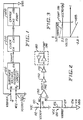
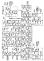
- FIG. 1 a block diagram shows the general structure of the oscillatorless substrate bias generator circuit of the present invention.
- a signal V BBREF (which is proportional to the substrate voltage V BB ) is input to a voltage regulator 100.
- the V BBREF signal is compared to a reference voltage V CCREF , preferably V CC /2, to determine whether the substrate voltage V BB has risen above a certain predetermined level (for example, approximately minus two (-2) volts). If substrate voltage V BB has risen above that level, regulator circuit 100 enables a clock circuit 200.
- Clock circuit 200 generates clock signals which control a charge pump 600 which pumps electrons to V BB (or draws current from V BB ) to lower the potential at V BB to a desired level.
- a simple schematic diagram is shown in Figure 2 to describe the operation of the substrate voltage regulator circuit 100 of Figure 1.
- the substrate voltage regulator circuit monitors the substrate voltage V BB to determine whether V BB has risen above a desired level.
- a resistor network 120 comprising resistors 122, 124 and 126 is used to generate a voltage V BBREF (which is proportional to the voltage at the substrate 128) at the negative input (node N1) of the differential amplifier 130.
- a second resistor network 110 comprising resistors 112 and 114 is used to generate a reference voltage V CCREF at the positive input (node N2) of the differential amplifier 130.
- V out 142 is passed through a series of inverters (150, 170 and 180 which will be discussed in detail in reference to Figure 4) to generate a pump signal 196. Therefore, when the V BB signal is insufficiently negative, the substrate voltage regulator circuit 100 will generate a high pump signal 196 to activate clock circuit 200 and charge pump 600. Otherwise, a low pump signal 196 disables clock circuit 200, and both the clock and the charge pump remain off.
- Figure 3 shows a timing diagram of the input and output signals of V BB regulator 100, and specifically shows when the pump signal 196 changes between high and low signals to enable or disable clock circuit 200 and charge pump 600.
- the timing diagram of Figure 3 includes a 5 volt V CC , a 3 volt V CC is also contemplated in the present invention.
- V CC is fixed, the positive input V CCREF to the differential amplifier is fixed at approximately at V CC /2 or 2.5 volts.
- V BBREF is dependent on V BB , and therefore may vary with the substrate voltage. When V BB is initially at 0 volts, V BBREF is at approximately 3.3 volts (assuming that resistances of 122, 124 and 126 are the same).
- V BBREF is greater than V CCREF
- the output of differential amplifier 130 will be low, and pump signal 196 will be high, activating the charge pump.
- V BB is gradually decreased by pumping charge (electrons) to the substrate
- V BBREF will gradually drop.
- V BBREF will drop below V CCREF . Therefore, the output of the differential amplifier will now be high and pump signal 196 will be low, thereby turning off the clock circuit which is connected to the charge pump.
- V BBREF later rises above V CCREF , the pump will again be turned on to lower the voltage of the substrate.
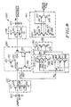
- transistor 124 of Figure 4 is a P channel enhancement type transistor with its substrate tied to its source.
- all transistors are preferably enhancement type transistors, although depletion type transistors could be used.
- the voltage regulator circuit 100 of Figure 4 is designed to generally operate on low current and limit current loss in the circuit.
- the resistor networks 110 and 120 include transistors configured as resistors (i.e. transistors having the gate tied to the source or drain). Because the current through the transistors is a function of the ratio of the channel width/length ratio, the channel lengths of these enhancement resistors are generally large to limit current through the transistor networks.
- the differential amplifier circuit 130 preferably includes transistors 132-140 configured to compare V CCREF with V BBREF and to provide an output (V out ) signal 142. The operation of differential amplifier circuit 130 is well known in the art.
- the preferred dimensions of the transistors 132-140 (shown in Appendix A) of the differential amplifier circuit 130 are specifically chosen to keep current in the circuit low, and therefore minimize power consumption. Specifically, the width/length ratio of the transistors of the differential amplifier circuit 130 is preferably kept small by selecting long channel lengths to limit the current flow. Although the specific design of differential amplifier circuit 130 is shown, other circuits which compare two signals to provide an output and limit current flow could be used within the scope of the present invention.
- a slow changing signal 142 i.e. a signal which does not have a sharp transition between low and high states.
- a slow changing signal can often lead to current loss in a circuit, particularly when input to a two transistor inverter. Specifically, both transistors of the inverter will be on for a certain period of time, leading to "through current” or “crow bar current” through the series of transistors. Therefore, there is often current loss from V CC to ground by way of the two transistors during the transition.
- inverters 150 and 170 and latch 180 are specifically designed to reduce the through current in the inverters and to output a pump signal 196 having a sharp transition.
- the switching time of transistors is generally dependent on the channel width/length ratio. Therefore, the channel widths and lengths can be chosen to establish when the transistors of the inverter will switch. Because the widths of the transistors in circuit 150 are the same, the switching time will be a function of their channel lengths.
- the channel lengths of the transistors of 154, 156, 164 and 166 of circuit 150 are chosen so that the voltages at nodes N4 and N5 (and therefore transistors 172 and 174 of circuit 170) switch at an appropriate time.
- V out signal 142 transitions from a high signal to a low signal to change the voltage at node N6 from high to low
- the length of transistor 166 is generally longer than that of transistor 154 to ensure that transistor 174 turns on after transistor 172 turns off.
- transistor 174 when V out transitions from a low signal to a high signal, it is beneficial to turn off transistor 174 before turning on transistor 172 to limit through current from V CC to ground.
- the length of transistor 156 is generally longer than that of transistor 168 to ensure that transistor 172 turns on after transistor 174 turns off. Therefore, the selection of channel lengths of the transistors of inverter circuit 150 eliminate any path from V CC to ground in inverter 170 during either transition.
- transistors 158 and 164 are added to inverter 150 to reduce any through current in inverters 153 and 163. Because of the current-limiting transistors 158 and 164 have long channel lengths, nodes N4 and N5 will not be pulled rapidly to ground and V CC , respectfully. Therefore, the path from V CC to ground will exist while driving transistors 172 and 174, but the current will be reduced in the series of transistors 154-158 and 164-168 by the long channel lengths of transistors 158 and 164.
- transistors 158 and 164 are selectively positioned to ensure that the timing of the switching of the transistors as described above is not affected.
- the inverter 153 drive N4 high very quickly by turning on transistor 154 to shut off transistor 172. Therefore, current-limiting transistor 158 is added only to the n-channel side of the inverter 153 to limit the effect of transistor 158 on transistor 154. While current-limiting transistor 158 does effect the timing of driving node N4 low when node N3 transitions from low to high, the capacitive coupling of transistor 158 to node N4 is large enough to pull node N4 low enough to turn on transistor 172 at an appropriate time.
- inverter 163 drive node N5 low very quickly by turning on transistor 168 to shut off transistor 174.
- the current-limiting transistor 164 is added only to the p-channel side of inverter 163 to limit the effect of transistor 164 on transistor 168. While current-limiting transistor 164 does affect the timing of driving node N5 high when node N3 transitions from high to low, the capacitive coupling of transistor 164 to node N5 is large enough to pull node N5 high enough to turn on transistor 174 at an appropriate time.
- latch 180 is also included in the voltage regulator circuit 100 to maintain the output of the pump signal 196 during the period when neither transistor 172 nor transistor 174 of inverter 170 is driven (as discussed above to prevent through current).
- Pump signal 196 is fed back via line 195 to transistor network 182-188 to maintain the original voltage at node N6 until the state of node N6 changes when inverter 170 drives node N6.
- latch 180 In order to reduce the power consumption of the oscillator, latch 180 itself is designed to limit the through current while also providing a weak latch.
- Transistors 172 and 174 are generally small transistors (i.e. small widths and lengths) to limit the current required from inverter 150 to switch inverter 170.
- they because of their size, they generally cannot drive a large capacitive load at node N6. Too large a capacitance at node N6 is undesirable because this capacitance will cause the voltage at the node to switch slowly. Therefore, a weak latch is provided at node N6 by selecting transistors 184 and 186 to have smaller widths and lengths, preferably on the order of 1-2 ⁇ m, to limit the capacitance at node N6.
- transistors 184 and 186 of the latch have widths and lengths which are about equal, they also have a large width/length ratio and drive greater current. Therefore, current-limiting transistors 182 and 188 are included. These transistors have long channel lengths (and therefore small width/length ratios) to limit the current in the latch 180 and reduce power consumption in the circuit.
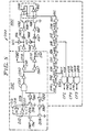
- clock circuit 200 Having generated a stable pump signal 196 in the voltage regulator circuit 100, a high pump signal 196 is used to activate clock circuit 200.
- clock circuit 200 generates signals which control charge pump 600.
- the first stage 202 of the clock circuit generates clock signals CP1 and CP1B, while the second stage 400 of the clock circuit receives signals CP1 and CP1B to generate signals CP2, CP3 and CP4. (It will be recognized that "B” stands for "bar” and denotes a complementary signal.)
- the signals generated by both stages of the clock circuit are used to drive the pump circuit 600.
- clock circuit 200 is a self-timed clock.
- the pump circuit operates on a two cycle principle: a pumping cycle and a precharge cycle. Therefore, the clock circuit must generate two sets of signals. While the clock circuit 200 generally operates in the same manner during both cycles, the circuit includes a feedback line to generate different signals during each cycle. The clock signals generated during the pump cycle will be described first, followed by the clock signals generated during the precharge cycle.
- signal V 11 a feedback input to the first stage 202, generally determines the cycle of the pumping circuit.
- the outputs of the clock circuit will be those present after a precharge cycle and when the circuit is waiting to receive a pump signal. Therefore, signal V 11 is high and transistor 208 is on, allowing the clock circuit 200 to receive the pump signal 196.
- the pump signal 196 is low, the clock circuit and the current pump remain in the quiescent state until receiving a high pump signal.
- CP1 and CP1B are used to drive the second stage 400 of the clock circuit and generate signals CP2, CP3 and CP4.
- CP1B and CP1 are input into inverters 410 and 460.
- These inverters along with associated capacitors 416 and 466 are a part of the self-timing circuitry of the clock circuit and are used as delay circuits.
- Inverters 410 and 460 include transistors having long channels which, along with capacitors 416 and 466, set the delay. The delay is necessary to set the time periods T PUMP and T PRECHARGE , shown in the timing diagram of Figure 9, to adequately pump all the charge during both cycles of the charge pump.
- the signals charging capacitors 416 and 466 are input into the Schmitt triggered inverters 420 and 470 respectively.
- a Schmitt trigger can change a slow moving waveform (such as the signals used to charge capacitors 416 and 466) into a waveform having a sharp transition.
- a latch circuit including inverters 440 and 450 is used to prevent the output from floating and to generate a stable output V 02 when neither transistor 438 nor transistor 488 is driving the output V 02 .
- the output of the latch is then transmitted through a series of inverters 500-548. These inverters generally provide delay and signal inversion for generating signals CP2, CP3 and CP4. Gates 550, 562 and 574 receive intermediate signals at various stages of the series of inverters to generate output signals CP2, CP4 and CP3, respectively. As is apparent from the circuit of Figure 5, CP2 and CP4 are identical signals. The need for identical signals will become more clear in the description of the pumping cycles of the pump circuit of Figure 8. Because NAND gate 574 is driven by signals which are separated by one additional inverter from the signals which drive NAND gates 550 and 562, CP2/4 and CP3 are non-overlapping active low signals which are 180° out of phase with each other. These non-overlapping signals are required (along with the CP1 and CP1B signals) to drive the pump circuit.
- the feedback signal V 11 is the inverted signal of the input V 02 (and the initial signal V 11 ).
- This feedback configuration of signal V 11 provides the self-timed feature of the present invention. Specifically, the inverted signal V 11 , which is low after the pumping cycle, turns off transistor 208 to ignore the pump signal 196 and to simultaneously begin the precharge cycle (i.e. generate clock signals CP1, CP1B, CP2, CP3 and CP4 used during the precharge). As a result, the clock circuit ignores the pump signal and ensures that the pump circuit remains in the precharge cycle for a required duration to transfer adequate charge to be pumped in the subsequent pumping cycle.
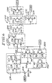
- FIGs 6 and 7 are detailed schematics of the first and second stages respectively of the charge pump of Figure 5. These figures show the commonly known configuration of transistors used to form the various gates shown in block form in Figure 5. For example, an inverter shown in block form is shown as a well known configuration of two transistors. While the operation of the clock circuit 200 is best described in reference to the block diagram of Figure 5, these figures are included to show the preferred schematic diagram of the clock circuit in detail, including the preferred dimensions of the transistors (set forth in Appendix A).
- the charge circuit is a two stage charge pump having capacitors 610 and 620 coupled to receive signals CP1 and CP1B. Signals CP1 and CP1B are used to change the voltages at nodes N2 and N1 when applied to capacitors 610 and 620. Capacitors 610 and 620 allow nodes N2 and N1 to be driven to a negative potential as is required to operate the charge pump. By changing the voltages at these nodes, charge (electrons) can be transferred along the path of transistors 630, 632 and 634 from ground to the substrate, ultimately to lower the voltage V BB at the substrate.
- the charge pump of the present invention is a two-stage charge pump
- charge at node N2 (stored during a previous pumping cycle) will be pumped to node N1 during the precharge cycle, before being pumped to the substrate during the pumping cycle.
- Signals CP2, CP3 and CP4 are used to regulate transistors 630, 632 and 634 during the pumping cycle to advance charge from GND to N2 and from N1 to V BB , and during the precharge cycle to advance charge from N2 to N1.
- Capacitors 652, 654 and 656 are also used to drive nodes N5, N3 and N4 to a negative potential to operate the charge pump. The operation of the pump circuit will be explained in more detail in reference to Figure 9.
- Figure 9 shows a timing diagram of the output signals of the clock circuit during a quiescent state (i.e. after a previous precharge cycle when the circuit is waiting for a pump signal), the pump cycle, the precharge cycle and a subsequent quiescent state.
- the reference to low or high clock signals is intended to mean ground potential or V CC , respectively, where V CC is preferably 3 volts or 5 volts. Voltages present during the two cycles at various nodes of the pump circuit (designated as N1-N5 in Figure 9) are also shown to provide a greater understanding of the operation of the two stage charge pump.
- the clock signals and the voltages at the nodes are at the state after the precharge cycle is completed (which will be described later in reference to the T PRECHARGE period). These clock signals and voltages will remain in that state until the clock circuit receives a signal to pump.
- the clock circuit receives a high pump signal to begin the pumping cycle.
- CP1 and CP1B gradually transition to high and low voltages respectively.
- CP2 and CP4 are low after the previous precharge cycle, turning on transistors 630 and 634. Because CP3 is high and transistor 632 is off, there is no direct path from ground to the substrate and there can be no undesired flow of charge.
- CP1 transition high the voltage at node N2 increases and draws negative charge from GND to node N 2 via transistor 630 (which is turned on with a low CP2 signal). Therefore, node N 2 gradually equalizes to ground potential.
- node N4 is coupled to node N1 by turning on transistor 646.
- transistor 646 When transistor 646 is on, the voltage at the gate of transistor 634 is clamped to its source, ensuring that transistor 634 remains off during the precharge.
- Node N4 is also coupled to node N1 during the precharge cycle by turning on transistor 646 in order to maintain node N4 at a voltage below ground potential.
- Node N4 is maintained below ground potential at approximately minus one (-1) volt to ensure that transistor 634 will turn on as CP4 transitions to a low level and all the charge is transferred to the substrate during the pumping cycle.
- transistor 644 is coupled to node N3, clamping N3 to ground potential during the pumping cycle to ensure that transistor 632 remains off and no charge is transferred from node N2 (or ground) to node N1. Therefore, during the pumping cycle, charge is pumped from ground to node N2 and from N1 to the substrate.
- time t2 marks the end of the pumping stage.
- signal CP3 transitions from high to low, preparing the circuit for the precharge cycle.
- Signal CP3 transitions after CP2 and CP4 transitions to provide a non-overlapping active low signal. Therefore, transistor 632 is not turned on by a low CP3 signal driving node N3 low until after transistors 630 and 634 are already turned off (i.e. when signals CP2 and CP4 previously transitioned from low to high at time t2). This timing prevents any undesirable current flow between ground and node N2 and node N1 and VBB.
- signal V11 goes low, marking the beginning of the precharge cycle.
- the clock circuit shown in Figure 5 ignores the pump signal during the precharge cycle as the pump circuit is preparing for a subsequent pump cycle (i.e. if the clock circuit should receive a pump signal after the precharge cycle is completed). This provides the self-timed feature by ensuring that pumping circuit is fully ready to pump when it receives a pumping signal.
- CP1 transitions to a low level and CP1B transitions to a high level. As these signals change, node N2 becomes more negative, while node N1 becomes more positive. Because CP3 is low, transistor 632 is on, allowing charge to be transferred from node N2 to node N1. However, transistors 630 and 634 are turned off with high CP2 and CP4 signals to prevent any undesired transfer of charge from ground to node N2 or from node N1 to the substrate.
- the pump circuit further includes transistors 646 and 650 to ensure that transistors 630 and 634 remain off during the precharge cycle. Specifically, transistors 646 and 650 clamp the gate voltages of transistors 630 and 634 at nodes N4 and N5 to their respective source voltages to prevent any undesired transfer of charge. When CP3 is low, transistor 650 is on and clamps node N5 to ground, ensuring that transistor 630 is off during the precharge. Also, transistor 646 is on during the pre-charge cycle to ensure that transistor 634 remains off. Transistor 646 also serves another function, previously discussed in regard to the pumping cycle.
- Transistor 646 clamps the voltage at node N4 to node N1 (at approximately minus one (-1) volt) to ensure that the voltage at node N4 is low enough so that transistor 634 will be turned on during a subsequent pumping cycle. Therefore, no charge is transferred between ground and node N2 or node N1 and the substrate. As is apparent near the end of the T PRECHARGE , the voltage at nodes N1 and N2 equalize at a resulting voltage of approximately minus one (-1) volt. As nodes N2 and N1 equalize, the charge pump is in a stable state for a subsequent pumping cycle, should the charge pump receive a pumping signal.
- CP3 transitions to a high level at a time t5, turning off transistor 632 and ending the precharge cycle.
- CP2 and CP4 transition low, turning on 630 and 634 to prepare for the next pumping cycle.
- the transition of the signals CP2, CP3 and CP4 is again chosen to prevent any undesired flow of current between ground and the substrate.
- signal V11 transitions to a high level, allowing the clock circuit to read the pump signal 196. If the pump signal is high, the clock circuit will generate the signals in the T PUMP cycle followed by the T PRECHARGE cycle. If the pump signal is low, the clock circuit remains in the quiescent state shown in T QUIESCENT until receiving a high pump signal.
- the circuit of the present invention provides a low current and low power dissipation substrate bias generator.
- the circuit is also draws low current by disabling the clock circuit and charge pump when in a standby mode.
- the circuit eliminates the need for a constantly running oscillator by providing a self-timed clock circuit. When this clock circuit receives an active pump signal, the clock circuit will generate signals to pump, followed by signals to restore the pump (i.e. during the precharge stage) to ensure adequate pumping during the subsequent pumping cycle.
- the self-timed feature of the clock allows the clock to ignore the pumping signal until the precharge cycle is complete.
- charge pump Any type of charge pump could be used within the scope of the present invention. Specifically, a single stage charge pump or a pump employing n-channel transistors could be used. Also, the voltage bias generator of the present invention could provide an oscillatorless pump drawing low current to pump charge to a node of an integrated circuit other than the substrate to maintain that node at a desired potential.
Landscapes
- Engineering & Computer Science (AREA)
- Power Engineering (AREA)
- Physics & Mathematics (AREA)
- Radar, Positioning & Navigation (AREA)
- Electromagnetism (AREA)
- General Physics & Mathematics (AREA)
- Automation & Control Theory (AREA)
- Microelectronics & Electronic Packaging (AREA)
- Nonlinear Science (AREA)
- Semiconductor Integrated Circuits (AREA)
- Dram (AREA)
- Dc-Dc Converters (AREA)
- Logic Circuits (AREA)
Claims (8)
- Générateur de polarisation de substrat pour un circuit intégré incluant un circuit de régulateur de tension faible courant (100) couplé au substrat (128) dudit circuit intégré pour surveiller la tension (VBB) au niveau du substrat (128) et pour émettre en sortie un signal de validation d'horloge (PMP) lorsque la tension (VBB) varie par rapport à un niveau prédéterminé et un circuit de pompage (600) pour commander ladite tension (VBB) au niveau du substrat, ledit générateur étant caractérisé en ce qu'il comprend :
un circuit d'horloge auto-cadencé faible courant (200) qui est synchronisé avec et sensible au signal de validation d'horloge (PMP) pour générer des signaux d'horloge (CP1-CP4), ledit circuit d'horloge (200) incluant un premier étage (202) pour recevoir le signal de validation d'horloge et pour émettre en sortie des premier et second signaux (CP1, CP1B) et un second étage (400) pour recevoir les premier et second signaux (CP1, CP1B) et pour émettre en outre en sortie des troisième, quatrième et cinquième signaux (CP2-CP4), un circuit de pompage (600) sensible aux premier à cinquième signaux (CP1-CP4) pour pomper une charge et abaisser la tension (VBB) du substrat (128) dudit circuit intégré, et dans lequel le circuit d'horloge auto-cadencé (200) ignore le signal de validation d'horloge (PMP) jusqu'à après la fin du pompage. - Générateur de polarisation de substrat pour un circuit intégré selon la revendication 1, caractérisé en ce que le circuit de régulateur de tension (100) comprend en outre un premier réseau de résistances (110) pour générer un signal de référence (VCCREF) proportionnel à un signal d'alimentation (VCC), un second réseau de résistances (120) pour générer un signal (VBBREF) proportionnel à la tension (VBB) au niveau du substrat (128), un circuit d'amplificateur différentiel (130) pour comparer le signal (VCCREF) proportionnel au signal d'alimentation (VCC) et le signal (VBBREF) proportionnel à la tension (VBB) au niveau du substrat (128), une série d'inverseurs (150, 170) couplés audit amplificateur différentiel (130) pour émettre en sortie un signal de validation d'horloge (PMP) lorsque le signal (VCCREF) proportionnel au signal d'alimentation (VCC) excède le signal (VBBREF) proportionnel à la tension (VBB) au niveau du substrat (128), et un circuit de bascule (180) couplé à ladite série d'inverseurs (150, 170) pour émettre en sortie un signal de validation d'horloge stable (PMP).
- Générateur de polarisation de substrat pour un circuit intégré selon l'une quelconque des revendications précédentes, caractérisé en ce que le circuit de pompage (600) est une pompe à deux étages incluant des transistors à canal P.
- Générateur de polarisation de substrat pour un circuit intégré selon l'une quelconque des revendications précédentes, caractérisé en ce que le circuit d'horloge auto-cadencé (200) est validé seulement lorsqu'il reçoit un signal de validation d'horloge actif (PMP).
- Procédé de régulation de la tension (VBB) du substrat (128) d'un dispositif de circuit intégré incluant l'étape de surveillance de la tension (VBB) au niveau dudit substrat (128), ledit procédé étant caractérisé par les étapes de :
validation d'un circuit d'horloge auto-cadencé (200) lorsque la tension (VBB) au niveau du substrat (128) varie par rapport à un niveau prédéterminé, pompage d'une charge sur le substrat (128) afin d'altérer la tension (VBB) au niveau du substrat (128) lorsque la tension (VBB) au niveau du substrat (128) varie par rapport à un niveau prédéterminé. - Procédé de régulation de la tension (VBB) du substrat (128) selon la revendication 5, caractérisé en ce que l'étape de surveillance de la tension inclut en outre la génération d'un premier signal de référence (VCCREF) proportionnel à un signal d'alimentation (VCC), la génération d'un second signal de référence (VBBREF) proportionnel à la tension (VBB) au niveau du substrat (128), la comparaison desdites première et seconde tensions de référence (VCCREF et VBBREF) et l'émission en sortie d'un signal de validation d'horloge (PMP) lorsque ladite première tension de référence (VBBREF) excède ladite seconde tension de référence (VCCREF).
- Procédé de régulation de la tension (VBB) du substrat (128) selon la revendication 5 ou 6, caractérisé en ce que l'étape de validation du circuit d'horloge (200) inclut la réception d'un signal de validation d'horloge actif (PMP) et l'émission en sortie de signaux d'horloge (CP1-CP4) pour commander le pompage de charge afin de pomper une charge sur le substrat (128).
- Procédé de régulation de la tension du substrat selon la revendication 5, 6 ou 7, dans lequel l'étape de pompage inclut la réception de signaux d'horloge (CP1-CP4) et l'abaissement de la tension (VBB) du substrat (128) dudit circuit intégré en utilisant une pompe à deux étages (600) incluant des transistors à canal P.
Applications Claiming Priority (2)
| Application Number | Priority Date | Filing Date | Title |
|---|---|---|---|
| US964912 | 1992-10-22 | ||
| US07/964,912 US5347172A (en) | 1992-10-22 | 1992-10-22 | Oscillatorless substrate bias generator |
Publications (2)
| Publication Number | Publication Date |
|---|---|
| EP0596228A1 EP0596228A1 (fr) | 1994-05-11 |
| EP0596228B1 true EP0596228B1 (fr) | 1997-08-06 |
Family
ID=25509149
Family Applications (1)
| Application Number | Title | Priority Date | Filing Date |
|---|---|---|---|
| EP93115067A Expired - Lifetime EP0596228B1 (fr) | 1992-10-22 | 1993-09-20 | Générateur de polarisation de substrat sans oscillateur |
Country Status (5)
| Country | Link |
|---|---|
| US (1) | US5347172A (fr) |
| EP (1) | EP0596228B1 (fr) |
| JP (1) | JP2889979B2 (fr) |
| KR (1) | KR100278870B1 (fr) |
| DE (1) | DE69312858T2 (fr) |
Cited By (1)
| Publication number | Priority date | Publication date | Assignee | Title |
|---|---|---|---|---|
| US6304467B1 (en) | 1999-06-25 | 2001-10-16 | The Procter & Gamble Company | Progressive start-up circuit for activating a charge pump |
Families Citing this family (29)
| Publication number | Priority date | Publication date | Assignee | Title |
|---|---|---|---|---|
| US6424202B1 (en) * | 1994-02-09 | 2002-07-23 | Lsi Logic Corporation | Negative voltage generator for use with N-well CMOS processes |
| JP3292417B2 (ja) * | 1994-02-15 | 2002-06-17 | 三菱電機株式会社 | 半導体装置 |
| KR0149224B1 (ko) * | 1994-10-13 | 1998-10-01 | 김광호 | 반도체 집적장치의 내부전압 승압회로 |
| US5670907A (en) * | 1995-03-14 | 1997-09-23 | Lattice Semiconductor Corporation | VBB reference for pumped substrates |
| US5973956A (en) * | 1995-07-31 | 1999-10-26 | Information Storage Devices, Inc. | Non-volatile electrically alterable semiconductor memory for analog and digital storage |
| US5694072A (en) * | 1995-08-28 | 1997-12-02 | Pericom Semiconductor Corp. | Programmable substrate bias generator with current-mirrored differential comparator and isolated bulk-node sensing transistor for bias voltage control |
| JPH09330590A (ja) * | 1996-06-07 | 1997-12-22 | Mitsubishi Electric Corp | 内部電圧検出回路、および基板電圧検出回路 |
| TW362277B (en) * | 1996-07-29 | 1999-06-21 | Hynix Semiconductor Inc | Charge pump for a semiconductor substrate |
| US6188590B1 (en) | 1996-12-18 | 2001-02-13 | Macronix International Co., Ltd. | Regulator system for charge pump circuits |
| WO1998027477A1 (fr) * | 1996-12-18 | 1998-06-25 | Macronix International Co., Ltd. | Systeme de regulation pour pompes a charge |
| KR100273208B1 (ko) * | 1997-04-02 | 2000-12-15 | 김영환 | 반도체메모리장치의고효율전하펌프회로 |
| JP3135859B2 (ja) * | 1997-04-11 | 2001-02-19 | 株式会社リコー | 基板バイアス回路 |
| FR2773012B1 (fr) | 1997-12-24 | 2001-02-02 | Sgs Thomson Microelectronics | Dispositif a pompe de charges negatives |
| FR2772941B1 (fr) * | 1998-05-28 | 2002-10-11 | Sgs Thomson Microelectronics | Circuit de regulation d'une pompe de charges negatives |
| CA2377166C (fr) | 1999-06-25 | 2006-05-30 | Dragan Danilo Nebrigic | Transformateur de courant continu a commutation dynamique |
| US6370046B1 (en) | 2000-08-31 | 2002-04-09 | The Board Of Trustees Of The University Of Illinois | Ultra-capacitor based dynamically regulated charge pump power converter |
| JP2001332696A (ja) | 2000-05-24 | 2001-11-30 | Nec Corp | 基板電位検知回路及び基板電位発生回路 |
| US6486727B1 (en) * | 2001-10-11 | 2002-11-26 | Pericom Semiconductor Corp. | Low-power substrate bias generator disabled by comparators for supply over-voltage protection and bias target voltage |
| DE10162309A1 (de) * | 2001-12-19 | 2003-07-03 | Philips Intellectual Property | Verfahren und Anordnung zur Erhöhung der Sicherheit von Schaltkreisen gegen unbefugten Zugriff |
| DE60218225T2 (de) * | 2002-01-23 | 2007-10-31 | Koninklijke Philips Electronics N.V. | Integrierte schaltung und batteriebetriebenes elektronisches gerät |
| US6864664B2 (en) * | 2003-06-06 | 2005-03-08 | Sony Corporation | Circuit for charging supplemental battery in portable electronic device |
| US7012461B1 (en) | 2003-12-23 | 2006-03-14 | Transmeta Corporation | Stabilization component for a substrate potential regulation circuit |
| US7129771B1 (en) * | 2003-12-23 | 2006-10-31 | Transmeta Corporation | Servo loop for well bias voltage source |
| US7649402B1 (en) * | 2003-12-23 | 2010-01-19 | Tien-Min Chen | Feedback-controlled body-bias voltage source |
| KR100732756B1 (ko) * | 2005-04-08 | 2007-06-27 | 주식회사 하이닉스반도체 | 전압 펌핑장치 |
| KR100718037B1 (ko) * | 2005-09-13 | 2007-05-14 | 주식회사 하이닉스반도체 | 반도체 메모리 장치의 기판 바이어스 전압 발생 회로 |
| US8098089B2 (en) * | 2006-07-28 | 2012-01-17 | Stmicroelectronics S.R.L. | Voltage booster |
| US9002447B2 (en) | 2013-03-14 | 2015-04-07 | Medtronic, Inc. | Implantable medical device having power supply for generating a regulated power supply |
| US12205663B2 (en) * | 2019-07-09 | 2025-01-21 | Arm Limited | Regulated negative charge pump circuitry and methods |
Family Cites Families (17)
| Publication number | Priority date | Publication date | Assignee | Title |
|---|---|---|---|---|
| US4142114A (en) * | 1977-07-18 | 1979-02-27 | Mostek Corporation | Integrated circuit with threshold regulation |
| US4356412A (en) * | 1979-03-05 | 1982-10-26 | Motorola, Inc. | Substrate bias regulator |
| JPS55162257A (en) * | 1979-06-05 | 1980-12-17 | Fujitsu Ltd | Semiconductor element having substrate bias generator circuit |
| JPS5785253A (en) * | 1980-11-17 | 1982-05-27 | Toshiba Corp | Semiconductor device |
| US4401897A (en) * | 1981-03-17 | 1983-08-30 | Motorola, Inc. | Substrate bias voltage regulator |
| US4739191A (en) * | 1981-04-27 | 1988-04-19 | Signetics Corporation | Depletion-mode FET for the regulation of the on-chip generated substrate bias voltage |
| US4553047A (en) * | 1983-01-06 | 1985-11-12 | International Business Machines Corporation | Regulator for substrate voltage generator |
| US4585954A (en) * | 1983-07-08 | 1986-04-29 | Texas Instruments Incorporated | Substrate bias generator for dynamic RAM having variable pump current level |
| US4581546A (en) * | 1983-11-02 | 1986-04-08 | Inmos Corporation | CMOS substrate bias generator having only P channel transistors in the charge pump |
| NL8701278A (nl) * | 1987-05-29 | 1988-12-16 | Philips Nv | Geintegreerde cmos-schakeling met een substraatvoorspanningsgenerator. |
| JPS6445157A (en) * | 1987-08-13 | 1989-02-17 | Toshiba Corp | Semiconductor integrated circuit |
| US4883976A (en) * | 1987-12-02 | 1989-11-28 | Xicor, Inc. | Low power dual-mode CMOS bias voltage generator |
| JP2568442B2 (ja) * | 1989-07-14 | 1997-01-08 | セイコー電子工業株式会社 | 半導体集積回路装置 |
| US5220534A (en) * | 1990-07-31 | 1993-06-15 | Texas Instruments, Incorporated | Substrate bias generator system |
| JP2870277B2 (ja) * | 1991-01-29 | 1999-03-17 | 日本電気株式会社 | ダイナミック型ランダムアクセスメモリ装置 |
| JPH04255989A (ja) * | 1991-02-07 | 1992-09-10 | Mitsubishi Electric Corp | 半導体記憶装置および内部電圧発生方法 |
| US5126590A (en) * | 1991-06-17 | 1992-06-30 | Micron Technology, Inc. | High efficiency charge pump |
-
1992
- 1992-10-22 US US07/964,912 patent/US5347172A/en not_active Expired - Lifetime
-
1993
- 1993-09-20 DE DE69312858T patent/DE69312858T2/de not_active Expired - Lifetime
- 1993-09-20 EP EP93115067A patent/EP0596228B1/fr not_active Expired - Lifetime
- 1993-10-08 JP JP5277923A patent/JP2889979B2/ja not_active Expired - Lifetime
- 1993-10-22 KR KR1019930022062A patent/KR100278870B1/ko not_active Expired - Lifetime
Cited By (2)
| Publication number | Priority date | Publication date | Assignee | Title |
|---|---|---|---|---|
| US6304467B1 (en) | 1999-06-25 | 2001-10-16 | The Procter & Gamble Company | Progressive start-up circuit for activating a charge pump |
| US6310789B1 (en) | 1999-06-25 | 2001-10-30 | The Procter & Gamble Company | Dynamically-controlled, intrinsically regulated charge pump power converter |
Also Published As
| Publication number | Publication date |
|---|---|
| EP0596228A1 (fr) | 1994-05-11 |
| KR940009802A (ko) | 1994-05-24 |
| US5347172A (en) | 1994-09-13 |
| JPH06303765A (ja) | 1994-10-28 |
| DE69312858D1 (de) | 1997-09-11 |
| DE69312858T2 (de) | 1998-02-19 |
| KR100278870B1 (ko) | 2001-01-15 |
| JP2889979B2 (ja) | 1999-05-10 |
Similar Documents
| Publication | Publication Date | Title |
|---|---|---|
| EP0596228B1 (fr) | Générateur de polarisation de substrat sans oscillateur | |
| EP0609497B1 (fr) | Dispositif et méthode pour maintenir une tension élévée pour applications à basse puissance | |
| US4970408A (en) | CMOS power-on reset circuit | |
| US6323722B1 (en) | Apparatus for translating a voltage | |
| US5280455A (en) | Voltage supply circuit for use in an integrated circuit | |
| EP0254212B1 (fr) | Circuit semi-conducteur MOS | |
| JP2638533B2 (ja) | 不揮発性メモリ用電圧ブースタ | |
| US20010052811A1 (en) | Charge pump circuit | |
| KR0142970B1 (ko) | 반도체 메모리 장치의 기준전압 발생회로 | |
| US5808460A (en) | Rapid power enabling circuit | |
| US6084386A (en) | Voltage generation circuit capable of supplying stable power supply voltage to load operating in response to timing signal | |
| US4952863A (en) | Voltage regulator with power boost system | |
| US6069536A (en) | Ring oscillator including chain of plural series-connected comparators controlling by clock | |
| US6272029B1 (en) | Dynamic regulation scheme for high speed charge pumps | |
| JP2008259420A (ja) | 半導体基板用のチャージポンプ | |
| US5751182A (en) | Rapid start-up circuit for voltage reference and method of operation | |
| US20240275282A1 (en) | Circuit and method for start-up of reference circuits in devices with a plurality of supply voltages | |
| US6636451B2 (en) | Semiconductor memory device internal voltage generator and internal voltage generating method | |
| KR20020078971A (ko) | 반도체 소자의 내부 전원 발생기 | |
| US7372321B2 (en) | Robust start-up circuit and method for on-chip self-biased voltage and/or current reference | |
| KR0144488B1 (ko) | 전하 펌프 회로 | |
| US6667609B2 (en) | Current generating device with reduced switching time from an energy saving mode | |
| US6548995B1 (en) | High speed bias voltage generating circuit | |
| US6225849B1 (en) | High speed, high precision, power supply and process independent boost level clamping technique | |
| US7148745B1 (en) | Sleep mode recovery |
Legal Events
| Date | Code | Title | Description |
|---|---|---|---|
| PUAI | Public reference made under article 153(3) epc to a published international application that has entered the european phase |
Free format text: ORIGINAL CODE: 0009012 |
|
| AK | Designated contracting states |
Kind code of ref document: A1 Designated state(s): DE FR GB IT NL |
|
| 17P | Request for examination filed |
Effective date: 19940614 |
|
| 17Q | First examination report despatched |
Effective date: 19960325 |
|
| GRAG | Despatch of communication of intention to grant |
Free format text: ORIGINAL CODE: EPIDOS AGRA |
|
| GRAG | Despatch of communication of intention to grant |
Free format text: ORIGINAL CODE: EPIDOS AGRA |
|
| GRAH | Despatch of communication of intention to grant a patent |
Free format text: ORIGINAL CODE: EPIDOS IGRA |
|
| GRAH | Despatch of communication of intention to grant a patent |
Free format text: ORIGINAL CODE: EPIDOS IGRA |
|
| GRAA | (expected) grant |
Free format text: ORIGINAL CODE: 0009210 |
|
| RAP1 | Party data changed (applicant data changed or rights of an application transferred) |
Owner name: NIPPON STEEL SEMICONDUCTOR CORPORATION Owner name: UNITED MEMORIES, INC. |
|
| AK | Designated contracting states |
Kind code of ref document: B1 Designated state(s): DE FR GB IT NL |
|
| REF | Corresponds to: |
Ref document number: 69312858 Country of ref document: DE Date of ref document: 19970911 |
|
| ITF | It: translation for a ep patent filed | ||
| ET | Fr: translation filed | ||
| PLBE | No opposition filed within time limit |
Free format text: ORIGINAL CODE: 0009261 |
|
| 26N | No opposition filed | ||
| REG | Reference to a national code |
Ref country code: GB Ref legal event code: 732E |
|
| NLS | Nl: assignments of ep-patents |
Owner name: MOSEL VITELIC, INC. |
|
| NLT1 | Nl: modifications of names registered in virtue of documents presented to the patent office pursuant to art. 16 a, paragraph 1 |
Owner name: NIPPON FOUNDRY INC.;UNITED MEMORIES, INC. |
|
| REG | Reference to a national code |
Ref country code: GB Ref legal event code: IF02 |
|
| REG | Reference to a national code |
Ref country code: FR Ref legal event code: TP Ref country code: FR Ref legal event code: CD |
|
| REG | Reference to a national code |
Ref country code: GB Ref legal event code: 732E |
|
| NLS | Nl: assignments of ep-patents |
Owner name: PROMOS TECHNOLOGIES INC. |
|
| REG | Reference to a national code |
Ref country code: FR Ref legal event code: TP |
|
| PGFP | Annual fee paid to national office [announced via postgrant information from national office to epo] |
Ref country code: NL Payment date: 20100924 Year of fee payment: 18 |
|
| PGFP | Annual fee paid to national office [announced via postgrant information from national office to epo] |
Ref country code: IT Payment date: 20100928 Year of fee payment: 18 |
|
| REG | Reference to a national code |
Ref country code: NL Ref legal event code: V1 Effective date: 20120401 |
|
| PG25 | Lapsed in a contracting state [announced via postgrant information from national office to epo] |
Ref country code: IT Free format text: LAPSE BECAUSE OF NON-PAYMENT OF DUE FEES Effective date: 20110920 |
|
| PG25 | Lapsed in a contracting state [announced via postgrant information from national office to epo] |
Ref country code: NL Free format text: LAPSE BECAUSE OF NON-PAYMENT OF DUE FEES Effective date: 20120401 |
|
| PGFP | Annual fee paid to national office [announced via postgrant information from national office to epo] |
Ref country code: GB Payment date: 20120731 Year of fee payment: 20 |
|
| PGFP | Annual fee paid to national office [announced via postgrant information from national office to epo] |
Ref country code: FR Payment date: 20121001 Year of fee payment: 20 |
|
| PGFP | Annual fee paid to national office [announced via postgrant information from national office to epo] |
Ref country code: DE Payment date: 20120927 Year of fee payment: 20 |
|
| REG | Reference to a national code |
Ref country code: DE Ref legal event code: R071 Ref document number: 69312858 Country of ref document: DE |
|
| REG | Reference to a national code |
Ref country code: DE Ref legal event code: R071 Ref document number: 69312858 Country of ref document: DE |
|
| REG | Reference to a national code |
Ref country code: GB Ref legal event code: PE20 Expiry date: 20130919 |
|
| PG25 | Lapsed in a contracting state [announced via postgrant information from national office to epo] |
Ref country code: DE Free format text: LAPSE BECAUSE OF EXPIRATION OF PROTECTION Effective date: 20130921 |
|
| PG25 | Lapsed in a contracting state [announced via postgrant information from national office to epo] |
Ref country code: GB Free format text: LAPSE BECAUSE OF EXPIRATION OF PROTECTION Effective date: 20130919 |