EP0600149A2 - Méthode de fabrication d'un transistor à induction statique auto-aligné - Google Patents
Méthode de fabrication d'un transistor à induction statique auto-aligné Download PDFInfo
- Publication number
- EP0600149A2 EP0600149A2 EP93109474A EP93109474A EP0600149A2 EP 0600149 A2 EP0600149 A2 EP 0600149A2 EP 93109474 A EP93109474 A EP 93109474A EP 93109474 A EP93109474 A EP 93109474A EP 0600149 A2 EP0600149 A2 EP 0600149A2
- Authority
- EP
- European Patent Office
- Prior art keywords
- layer
- forming
- transistor
- metal
- polysilicon
- Prior art date
- Legal status (The legal status is an assumption and is not a legal conclusion. Google has not performed a legal analysis and makes no representation as to the accuracy of the status listed.)
- Granted
Links
Images



Classifications
-
- H—ELECTRICITY
- H10—SEMICONDUCTOR DEVICES; ELECTRIC SOLID-STATE DEVICES NOT OTHERWISE PROVIDED FOR
- H10D—INORGANIC ELECTRIC SEMICONDUCTOR DEVICES
- H10D30/00—Field-effect transistors [FET]
- H10D30/01—Manufacture or treatment
- H10D30/012—Manufacture or treatment of static induction transistors [SIT], e.g. permeable base transistors [PBT]
-
- H—ELECTRICITY
- H10—SEMICONDUCTOR DEVICES; ELECTRIC SOLID-STATE DEVICES NOT OTHERWISE PROVIDED FOR
- H10D—INORGANIC ELECTRIC SEMICONDUCTOR DEVICES
- H10D64/00—Electrodes of devices having potential barriers
- H10D64/01—Manufacture or treatment
- H10D64/021—Manufacture or treatment using multiple gate spacer layers, e.g. bilayered sidewall spacers
-
- H—ELECTRICITY
- H10—SEMICONDUCTOR DEVICES; ELECTRIC SOLID-STATE DEVICES NOT OTHERWISE PROVIDED FOR
- H10D—INORGANIC ELECTRIC SEMICONDUCTOR DEVICES
- H10D64/00—Electrodes of devices having potential barriers
- H10D64/20—Electrodes characterised by their shapes, relative sizes or dispositions
- H10D64/27—Electrodes not carrying the current to be rectified, amplified, oscillated or switched, e.g. gates
- H10D64/311—Gate electrodes for field-effect devices
- H10D64/411—Gate electrodes for field-effect devices for FETs
- H10D64/511—Gate electrodes for field-effect devices for FETs for IGFETs
- H10D64/512—Disposition of the gate electrodes, e.g. buried gates
- H10D64/513—Disposition of the gate electrodes, e.g. buried gates within recesses in the substrate, e.g. trench gates, groove gates or buried gates
-
- H—ELECTRICITY
- H10—SEMICONDUCTOR DEVICES; ELECTRIC SOLID-STATE DEVICES NOT OTHERWISE PROVIDED FOR
- H10P—GENERIC PROCESSES OR APPARATUS FOR THE MANUFACTURE OR TREATMENT OF DEVICES COVERED BY CLASS H10
- H10P14/00—Formation of materials, e.g. in the shape of layers or pillars
- H10P14/40—Formation of materials, e.g. in the shape of layers or pillars of conductive or resistive materials
- H10P14/416—Formation of materials, e.g. in the shape of layers or pillars of conductive or resistive materials of highly doped semiconductor materials, e.g. polysilicon layers or amorphous silicon layers
-
- H—ELECTRICITY
- H10—SEMICONDUCTOR DEVICES; ELECTRIC SOLID-STATE DEVICES NOT OTHERWISE PROVIDED FOR
- H10P—GENERIC PROCESSES OR APPARATUS FOR THE MANUFACTURE OR TREATMENT OF DEVICES COVERED BY CLASS H10
- H10P50/00—Etching of wafers, substrates or parts of devices
-
- H—ELECTRICITY
- H10—SEMICONDUCTOR DEVICES; ELECTRIC SOLID-STATE DEVICES NOT OTHERWISE PROVIDED FOR
- H10P—GENERIC PROCESSES OR APPARATUS FOR THE MANUFACTURE OR TREATMENT OF DEVICES COVERED BY CLASS H10
- H10P76/00—Manufacture or treatment of masks on semiconductor bodies, e.g. by lithography or photolithography
- H10P76/20—Manufacture or treatment of masks on semiconductor bodies, e.g. by lithography or photolithography of masks comprising organic materials
- H10P76/204—Manufacture or treatment of masks on semiconductor bodies, e.g. by lithography or photolithography of masks comprising organic materials of organic photoresist masks
Definitions
- the present invention relates to semiconductor transistors, and more particularly, to a method of making self aligned static induction transistors.
- the present invention provides for a method of fabricating self aligned static induction transistors.
- the method is comprised of the following steps. Fabricating an N silicon on N ⁇ silicon substrate. Forming an active area on the substrate. Forming a guard ring surrounding the active area. Forming an N+ polysilicon layer having an N+ layer adjacent the substrate that comprises source and gate regions of the transistor. Forming an oxide layer on top of the N+ polysilicon layer. Forming a second polysilicon layer on top of the oxide layer. Forming an oxide layer on top of the second polysilicon layer. Forming a self aligning mask on the second oxide layer. Forming trenches in the substrate using the self aligning mask. Forming gate regions at the bottom of the trenches.
- the present method employs only one minimum geometry mask, namely the trench mask. All of the key features of the transistor are defined by the trench mask and related processing parameters. Because of the self alignment achieved by the present invention, the number of channels per unit area is higher, which results in higher transconductance. In addition, some of the parasitic capacitance normally found in static induction transistors is also eliminated by the present invention.
- the static induction transistors produced by the present invention are faster and handle more power than their non-self aligned counterparts.
- variable sidewall trench oxide thickness This allows fabrication of static induction transistors with higher or lower breakdown voltages according to the thickness that is chosen. Thicker oxides allow for a more graded P gate junction. Furthermore, by providing a relatively thick N+ polysilicon layer allows for overetching of the first layer of metal, which provides for control of parasitic capacitance and resistance characteristics of the transistor.
- Fig. 1 shows an exposed top view of a representation of a self aligned static induction transistor 10 made in accordance with a processing method 40 (Fig. 12) of the present invention.
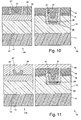
- Figs. 2-11 show relevant steps in the processing method 40 that produces the self aligned static induction transistor 10.
- FIG. 1 shows an N+ silicon substrate 11 having an epitaxial layer of N silicon 12 on a top surface thereof.
- a guard ring 15 is shown surrounding an active area 14a (stippled area) of the transistor 10.
- the active area 14a is derived from etching a larger active area 14 which is reduced in size by the etching procedure.
- a P+ trench 21 is shown having relatively long, narrow strips comprising an N+ polysilicon layer 16 that are the source and gate regions of the transistor 10. Also shown are a polysilicon mask 32 and a prepad mask 33 that will be described below with reference to the processing steps in the present method 40.
- Figs. 2-11 show cross sections, taken along the lines A-A (in the active area 14a) and B-B (in field region 14b) in Fig. 1, during the processing method 40.
- the N+ silicon substrate 11 is processed to grow the epitaxial layer of N silicon 12 on the top surface thereof.
- the N+ silicon substrate 11 comprises a drain (or drain region) of the transistor 10.
- a thermal oxide layer comprising a pad oxide (not shown) is grown on top of the epitaxial layer of N silicon 12, and a silicon nitride layer 13 is deposited onto the thermal oxide layer.
- An active area mask (not shown) is then deposited on top of the silicon nitride layer 13.
- the active area 14 is etched through the nitride layer 13 using the active area mask.
- the active area mask is then removed.
- a guard ring mask (not shown) is then formed over the top surface of the transistor 10.
- the guard ring 15 is implanted around the active area 14 of the transistor 10 through the guard ring mask.
- a field oxide layer 29 is then grown over the top surface of the field region 14b, which shrinks the active area 14 to a smaller sire, indicated by the active area 14a (shown stippled in Fig. 1).
- the nitride layer 13 is then stripped.
- the above processing steps are generally performed in fabricating conventional self aligned static induction transistors 10.
- an undoped polysilicon layer is then deposited on top of the transistor 10 after the nitride layer 13 pad oxide layer have been stripped.
- the undoped polysilicon layer is deposited to a thickness of 1 or more microns.
- the undoped polysilicon layer is then implanted with N+ dopant ions to produce an N+ polysilicon layer 16, and an N+ nitride layer 13 adjacent the substrate 11.
- the N+ polysilicon layer 16 subsequently becomes source and gate regions of the transistor 10.
- a relatively thick N+ polysilicon layer 16 is provided and allows for subsequent overetching of gate metal, as will be described below. This provides for control of parasitic capacitance and resistance characteristics of the transistor 10.
- Thermal oxide is then grown over the N+ polysilicon layer 16 to a thickness on the order of 500 ⁇ , and additional oxide is deposited on top of the thermal oxide to a thickness of about 4000 ⁇ to form a relatively thick oxide layer 17.
- a second layer of polysilicon 18 is deposited on top of the thermal oxide layer 17 using a low temperature deposition procedure.
- the second layer of polysilicon 18 is typically on the order of 3000 ⁇ thick.
- a high temperature dry oxidation procedure is employed to form a second oxide layer 19 on top of the second layer of polysilicon 18.
- the second oxide layer 19 is typically on the order of 600 ⁇ thick.
- a back etch procedure is then used to remove the second layer of polysilicon 18 and the relatively thick oxide layer 17 prior to subsequent processing off the back of the wafer.
- the back etch procedure may use plasma or a wet etch, for example.
- a trench mask 20 is formed over the surface of the transistor 10, and referring to Fig. 3, the trenches 21 are formed in the epitaxial layer of N silicon 12.
- the trenches 21 are etched using an anisotropic etching procedure which etches through the second oxide layer 19, the second layer of polysilicon 18, and the thick oxide layer 17, to the surface of the N+ polysilicon layer 16.
- a trencher is then used to trench into the N+ polysilicon layer 16 and into the epitaxial layer of N silicon 12.
- the anisotropic etching procedure produces a vertical sidewalls in the trenches 21.
- a post trench stripping procedure is used to remove the oxide on the sidewalls of the trenches 21. This stripping procedure may use diluted hydrofluoric acid, for example.
- a second layer of thermal oxide 22 is grown in the trenches 21, along the sidewalls of the trenches 21, and on top of the relatively thick oxide layer 17, which completely oxidizes the second layer of polysilicon 18.
- the oxidized second layer of polysilicon 18 is thus merged into the second layer of thermal oxide 22.
- the second layer of thermal oxide 22 is typically on the order of 6000 ⁇ thick.
- the second layer of thermal oxide 22 is etched using an anisotropic dry etch, for example. This etching procedure tapers the sidewalls of the second layer of thermal oxide 22 along the sidewalls of the trenches 21. The topmost portion of the second layer of thermal oxide 22 is removed, the trench sidewalls are tapered, and the epitaxial layer of N silicon 12 is exposed at the bottom of the trenches 21.
- a layer of gate oxide 23 is grown on top of the exposed layer of N silicon 12.
- the layer of gate oxide 23 is typically on the order of 210 ⁇ thick.
- a P-grade implant and annealing procedure is performed to produce a P-grade layer 25.
- the annealing procedure occurs at a temperature of about 1050 degrees Celsius, for about 30 minutes.
- P+ dopant ions are implanted into the P-grade layer 25 to form gate regions 26 of the transistor 10 and the transistor structure is annealed using a rapid thermal annealing procedure.
- the rapid thermal annealing occurs at a temperature of about 1100 degrees Celsius, for about 10 seconds.
- a wet oxide stripping procedure is then performed to strip the gate oxide layer 23 from the gate regions 26 of the transistor 10.
- variable sidewall trench oxide thickness provided the second layer of thermal oxide 22.
- the ability to provide for variable sidewall trench oxide thickness allows fabrication of static induction transistors 10 with higher or lower breakdown voltages according to the thickness that is chosen.
- a thicker layer of thermal oxide 22 along the sidewalls allows for a more graded P+ gate junction.
- a first layer of metal 27 is then deposited on top of the transistor 10 and into the trench 21 to make contact with the gate regions 26.
- the first layer of metal 27 is deposited to a thickness on the order of 5000 ⁇ .
- photoresist 28 is deposited over the top surface of the transistor 10, and the photoresist 28 is planarized. Then, the first layer of metal 27 along with the planarized layer of photoresist 28 are planarized to produce the structure shown in Fig. 8.
- the first layer of metal 27 is etched using a dry or wet etch, for example, to a predetermined depth below the top surface of the trench 21. The depth to which the metal is removed is not significant.
- This etching procedure produces the structure shown in Fig. 9.
- the photoresist 28 is stripped from the transistor 10 using O2 plasma, for example.
- a plasma nitride layer 31 is deposited onto the top surface of the transistor 10.
- the plasma nitride layer 31 is then planarized.
- the polysilicon mask 32 (Fig. 1) is then deposited onto the top surface of the transistor 10, and the plasma nitride layer 31 and the polysilicon mask 32 are etched to expose the gate metal disposed on the field oxide.
- a prepad mask 33 (Fig. 1) is formed over the undoped oxide layer and the oxide is etched and the mask is stripped.
- a second metal layer 34 is then deposited on the top surface of the transistor 10.
- the second metal layer 34 connects to respective source and gate regions of the transistor 10.
- the second metal layer 34 is then masked using a metal mask (not shown) to form a metal pad.
- a passivation layer (not shown) is deposited on top of the masked second metal layer 34.
- the passivation layer is masked using a passivation mask (not shown), and an interconnecting pad is formed by etching through the passivation layer. This completes fabrication of the transistor 10.
- Fig. 12 shows a flow diagram summarizing the steps in the method 40 of the present invention.
- the processing steps are as follows. Fabricating an N silicon on N ⁇ silicon substrate 11, indicated in step 41. Forming an active area 14 on the substrate 11, indicated in step 42. Forming a guard ring 15 surrounding the active area 14, indicated in step 43. Forming an N+ polysilicon layer 16 on the substrate 11 that comprises source and gate regions of the transistor 10, indicated in step 44. Forming an N+ layer 13 on the N+ polysilicon layer 16, indicated in step 45. Forming an oxide layer 17 on top of the N+ polysilicon layer 16, indicated in step 46. Forming a second polysilicon layer 18 on top of the layer of oxide 17 indicated in step 47.
- the present method 40 provides for the fabrication of a self aligned static induction transistor, and the transistor 10 is fabricated using one minimum geometry mask (the trench mask 20).
- the present invention provides for higher transconductance and f t in the fabricated static induction transistor 10.
- the unity gain frequency, or cutoff frequency (f t ) of the fabricated static induction transistor 10 is increased, resulting in a faster speed of operation, on the order of several gigahertz.
- the present invention also provides for variable operational voltage by controlling the sidewall thickness of the trench 21.
Landscapes
- Junction Field-Effect Transistors (AREA)
Applications Claiming Priority (2)
| Application Number | Priority Date | Filing Date | Title |
|---|---|---|---|
| US07/981,032 US5260227A (en) | 1992-11-24 | 1992-11-24 | Method of making a self aligned static induction transistor |
| US981032 | 1992-11-24 |
Publications (3)
| Publication Number | Publication Date |
|---|---|
| EP0600149A2 true EP0600149A2 (fr) | 1994-06-08 |
| EP0600149A3 EP0600149A3 (en) | 1995-11-29 |
| EP0600149B1 EP0600149B1 (fr) | 1999-02-10 |
Family
ID=25528048
Family Applications (1)
| Application Number | Title | Priority Date | Filing Date |
|---|---|---|---|
| EP93109474A Expired - Lifetime EP0600149B1 (fr) | 1992-11-24 | 1993-06-14 | Méthode de fabrication d'un transistor à induction statique auto-aligné |
Country Status (6)
| Country | Link |
|---|---|
| US (1) | US5260227A (fr) |
| EP (1) | EP0600149B1 (fr) |
| JP (1) | JPH077158A (fr) |
| KR (1) | KR970004845B1 (fr) |
| DE (1) | DE69323476T2 (fr) |
| TW (1) | TW280009B (fr) |
Families Citing this family (12)
| Publication number | Priority date | Publication date | Assignee | Title |
|---|---|---|---|---|
| US5283201A (en) * | 1988-05-17 | 1994-02-01 | Advanced Power Technology, Inc. | High density power device fabrication process |
| DE69628069T2 (de) * | 1995-03-13 | 2004-04-08 | Raytheon Co., Lexington | Verfahren zur Herstellung eines selbstjustierenden statischen Induktionstransistors |
| US5807773A (en) * | 1996-07-30 | 1998-09-15 | Northrop Grumman Corporation | Self-aligned gate fabrication process for silicon carbide static induction transistors |
| US5702987A (en) * | 1996-08-26 | 1997-12-30 | Chartered Semiconductor Manufacturing Pte Ltd | Method of manufacture of self-aligned JFET |
| US6855970B2 (en) | 2002-03-25 | 2005-02-15 | Kabushiki Kaisha Toshiba | High-breakdown-voltage semiconductor device |
| JP4623956B2 (ja) * | 2003-11-12 | 2011-02-02 | 株式会社豊田中央研究所 | Igbt |
| US7187021B2 (en) * | 2003-12-10 | 2007-03-06 | General Electric Company | Static induction transistor |
| US7750447B2 (en) * | 2007-06-11 | 2010-07-06 | Alpha & Omega Semiconductor, Ltd | High voltage and high power boost converter with co-packaged Schottky diode |
| US8008897B2 (en) * | 2007-06-11 | 2011-08-30 | Alpha & Omega Semiconductor, Ltd | Boost converter with integrated high power discrete FET and low voltage controller |
| US8021563B2 (en) | 2007-03-23 | 2011-09-20 | Alpha & Omega Semiconductor, Ltd | Etch depth determination for SGT technology |
| US7521332B2 (en) * | 2007-03-23 | 2009-04-21 | Alpha & Omega Semiconductor, Ltd | Resistance-based etch depth determination for SGT technology |
| US8456141B2 (en) | 2007-06-11 | 2013-06-04 | Alpha & Omega Semiconductor, Inc. | Boost converter with integrated high power discrete FET and low voltage controller |
Family Cites Families (11)
| Publication number | Priority date | Publication date | Assignee | Title |
|---|---|---|---|---|
| FR2507821A1 (fr) * | 1981-06-16 | 1982-12-17 | Thomson Csf | Transistor a effet de champ vertical a jonction et procede de fabrication |
| US4566172A (en) * | 1984-02-24 | 1986-01-28 | Gte Laboratories Incorporated | Method of fabricating a static induction type recessed junction field effect transistor |
| US4543706A (en) * | 1984-02-24 | 1985-10-01 | Gte Laboratories Incorporated | Fabrication of junction field effect transistor with filled grooves |
| US4611384A (en) * | 1985-04-30 | 1986-09-16 | Gte Laboratories Incorporated | Method of making junction field effect transistor of static induction type |
| US4713358A (en) * | 1986-05-02 | 1987-12-15 | Gte Laboratories Incorporated | Method of fabricating recessed gate static induction transistors |
| US5082795A (en) * | 1986-12-05 | 1992-01-21 | General Electric Company | Method of fabricating a field effect semiconductor device having a self-aligned structure |
| US5164325A (en) * | 1987-10-08 | 1992-11-17 | Siliconix Incorporated | Method of making a vertical current flow field effect transistor |
| JPH02143564A (ja) * | 1988-11-25 | 1990-06-01 | Matsushita Electric Works Ltd | 静電誘導サイリスタの製造方法 |
| JPH0817241B2 (ja) * | 1989-01-18 | 1996-02-21 | 日本電気株式会社 | 細線電界効果トランジスタ及びその製造方法 |
| US5143859A (en) * | 1989-01-18 | 1992-09-01 | Mitsubishi Denki Kabushiki Kaisha | Method of manufacturing a static induction type switching device |
| US5169795A (en) * | 1989-02-28 | 1992-12-08 | Small Power Communication Systems Research Laboratories Co., Ltd. | Method of manufacturing step cut type insulated gate SIT having low-resistance electrode |
-
1992
- 1992-11-24 US US07/981,032 patent/US5260227A/en not_active Expired - Fee Related
-
1993
- 1993-06-14 EP EP93109474A patent/EP0600149B1/fr not_active Expired - Lifetime
- 1993-06-14 DE DE69323476T patent/DE69323476T2/de not_active Expired - Fee Related
- 1993-06-15 JP JP5144031A patent/JPH077158A/ja active Pending
- 1993-06-15 KR KR1019930010841A patent/KR970004845B1/ko not_active Expired - Fee Related
- 1993-07-12 TW TW082105540A patent/TW280009B/zh active
Also Published As
| Publication number | Publication date |
|---|---|
| KR950002064A (ko) | 1995-01-04 |
| EP0600149A3 (en) | 1995-11-29 |
| JPH077158A (ja) | 1995-01-10 |
| US5260227A (en) | 1993-11-09 |
| EP0600149B1 (fr) | 1999-02-10 |
| DE69323476T2 (de) | 1999-09-02 |
| TW280009B (fr) | 1996-07-01 |
| KR970004845B1 (ko) | 1997-04-04 |
| DE69323476D1 (de) | 1999-03-25 |
Similar Documents
| Publication | Publication Date | Title |
|---|---|---|
| US6489652B1 (en) | Trench DMOS device having a high breakdown resistance | |
| US4417385A (en) | Processes for manufacturing insulated-gate semiconductor devices with integral shorts | |
| US4992390A (en) | Trench gate structure with thick bottom oxide | |
| US4641416A (en) | Method of making an integrated circuit structure with self-aligned oxidation to isolate extrinsic base from emitter | |
| JP2812811B2 (ja) | 半導体装置のフィールド酸化膜形成方法 | |
| JPS6150394B2 (fr) | ||
| JPH0851216A (ja) | メサ分離soiトランジスタおよびそれの製造方法 | |
| JPH0821613B2 (ja) | Mos装置の分離構造の製造方法 | |
| US5260227A (en) | Method of making a self aligned static induction transistor | |
| EP0409132B1 (fr) | Méthode de fabrication d'une structure comprenant des jonctions diffusées auto-alignées | |
| US5006911A (en) | Transistor device with high density contacts | |
| JPH07326663A (ja) | ウエハの誘電体分離方法 | |
| US5972777A (en) | Method of forming isolation by nitrogen implant to reduce bird's beak | |
| EP0732734B1 (fr) | Méthode de fabrication d'un transistor à induction statique auto-aligné | |
| EP0641022B1 (fr) | Structure d'isolation et procédé de sa fabrication | |
| EP0540262A2 (fr) | Isolation à ramure | |
| EP1032028B1 (fr) | Dispositif MOS amélioré à tranchée | |
| US3998674A (en) | Method for forming recessed regions of thermally oxidized silicon and structures thereof utilizing anisotropic etching | |
| US5763316A (en) | Substrate isolation process to minimize junction leakage | |
| EP0239384A2 (fr) | Procédé pour isoler les dispositifs semi-conducteurs dans un substrat | |
| EP0225426A2 (fr) | Procédé pour fabriquer un transistor du type MOS sur un substrat | |
| US5668043A (en) | Method for forming isolated regions in a semiconductor device | |
| US5268314A (en) | Method of forming a self-aligned bipolar transistor | |
| US7244641B2 (en) | Process sequence and mask layout to reduce junction leakage for a dual gate MOSFET device | |
| US5013672A (en) | Manufacturing process for high-frequency bipolar transistors |
Legal Events
| Date | Code | Title | Description |
|---|---|---|---|
| PUAI | Public reference made under article 153(3) epc to a published international application that has entered the european phase |
Free format text: ORIGINAL CODE: 0009012 |
|
| 17P | Request for examination filed |
Effective date: 19930614 |
|
| AK | Designated contracting states |
Kind code of ref document: A2 Designated state(s): DE FR GB |
|
| PUAL | Search report despatched |
Free format text: ORIGINAL CODE: 0009013 |
|
| AK | Designated contracting states |
Kind code of ref document: A3 Designated state(s): DE FR GB |
|
| 17Q | First examination report despatched |
Effective date: 19970707 |
|
| GRAG | Despatch of communication of intention to grant |
Free format text: ORIGINAL CODE: EPIDOS AGRA |
|
| GRAG | Despatch of communication of intention to grant |
Free format text: ORIGINAL CODE: EPIDOS AGRA |
|
| GRAH | Despatch of communication of intention to grant a patent |
Free format text: ORIGINAL CODE: EPIDOS IGRA |
|
| GRAH | Despatch of communication of intention to grant a patent |
Free format text: ORIGINAL CODE: EPIDOS IGRA |
|
| GRAA | (expected) grant |
Free format text: ORIGINAL CODE: 0009210 |
|
| RAP1 | Party data changed (applicant data changed or rights of an application transferred) |
Owner name: RAYTHEON COMPANY |
|
| AK | Designated contracting states |
Kind code of ref document: B1 Designated state(s): DE FR GB |
|
| REF | Corresponds to: |
Ref document number: 69323476 Country of ref document: DE Date of ref document: 19990325 |
|
| ET | Fr: translation filed | ||
| PLBE | No opposition filed within time limit |
Free format text: ORIGINAL CODE: 0009261 |
|
| STAA | Information on the status of an ep patent application or granted ep patent |
Free format text: STATUS: NO OPPOSITION FILED WITHIN TIME LIMIT |
|
| 26N | No opposition filed | ||
| REG | Reference to a national code |
Ref country code: GB Ref legal event code: IF02 |
|
| PGFP | Annual fee paid to national office [announced via postgrant information from national office to epo] |
Ref country code: FR Payment date: 20040513 Year of fee payment: 12 |
|
| PGFP | Annual fee paid to national office [announced via postgrant information from national office to epo] |
Ref country code: GB Payment date: 20040517 Year of fee payment: 12 |
|
| PGFP | Annual fee paid to national office [announced via postgrant information from national office to epo] |
Ref country code: DE Payment date: 20040520 Year of fee payment: 12 |
|
| PG25 | Lapsed in a contracting state [announced via postgrant information from national office to epo] |
Ref country code: GB Free format text: LAPSE BECAUSE OF NON-PAYMENT OF DUE FEES Effective date: 20050614 |
|
| PG25 | Lapsed in a contracting state [announced via postgrant information from national office to epo] |
Ref country code: DE Free format text: LAPSE BECAUSE OF NON-PAYMENT OF DUE FEES Effective date: 20060103 |
|
| PG25 | Lapsed in a contracting state [announced via postgrant information from national office to epo] |
Ref country code: FR Free format text: LAPSE BECAUSE OF NON-PAYMENT OF DUE FEES Effective date: 20060228 |
|
| GBPC | Gb: european patent ceased through non-payment of renewal fee |
Effective date: 20050614 |
|
| REG | Reference to a national code |
Ref country code: FR Ref legal event code: ST Effective date: 20060228 |