EP0600664A2 - Procédé d'attaque sèche pour une couche mince de silicium - Google Patents
Procédé d'attaque sèche pour une couche mince de silicium Download PDFInfo
- Publication number
- EP0600664A2 EP0600664A2 EP93309400A EP93309400A EP0600664A2 EP 0600664 A2 EP0600664 A2 EP 0600664A2 EP 93309400 A EP93309400 A EP 93309400A EP 93309400 A EP93309400 A EP 93309400A EP 0600664 A2 EP0600664 A2 EP 0600664A2
- Authority
- EP
- European Patent Office
- Prior art keywords
- gas
- layer
- etching
- silicon layer
- freon
- Prior art date
- Legal status (The legal status is an assumption and is not a legal conclusion. Google has not performed a legal analysis and makes no representation as to the accuracy of the status listed.)
- Granted
Links
Images

Classifications
-
- H—ELECTRICITY
- H10—SEMICONDUCTOR DEVICES; ELECTRIC SOLID-STATE DEVICES NOT OTHERWISE PROVIDED FOR
- H10D—INORGANIC ELECTRIC SEMICONDUCTOR DEVICES
- H10D30/00—Field-effect transistors [FET]
- H10D30/01—Manufacture or treatment
- H10D30/021—Manufacture or treatment of FETs having insulated gates [IGFET]
- H10D30/031—Manufacture or treatment of FETs having insulated gates [IGFET] of thin-film transistors [TFT]
- H10D30/0312—Manufacture or treatment of FETs having insulated gates [IGFET] of thin-film transistors [TFT] characterised by the gate electrodes
- H10D30/0316—Manufacture or treatment of FETs having insulated gates [IGFET] of thin-film transistors [TFT] characterised by the gate electrodes of lateral bottom-gate TFTs comprising only a single gate
-
- H—ELECTRICITY
- H10—SEMICONDUCTOR DEVICES; ELECTRIC SOLID-STATE DEVICES NOT OTHERWISE PROVIDED FOR
- H10D—INORGANIC ELECTRIC SEMICONDUCTOR DEVICES
- H10D30/00—Field-effect transistors [FET]
- H10D30/01—Manufacture or treatment
- H10D30/021—Manufacture or treatment of FETs having insulated gates [IGFET]
- H10D30/031—Manufacture or treatment of FETs having insulated gates [IGFET] of thin-film transistors [TFT]
- H10D30/0321—Manufacture or treatment of FETs having insulated gates [IGFET] of thin-film transistors [TFT] comprising silicon, e.g. amorphous silicon or polysilicon
-
- H—ELECTRICITY
- H10—SEMICONDUCTOR DEVICES; ELECTRIC SOLID-STATE DEVICES NOT OTHERWISE PROVIDED FOR
- H10P—GENERIC PROCESSES OR APPARATUS FOR THE MANUFACTURE OR TREATMENT OF DEVICES COVERED BY CLASS H10
- H10P50/00—Etching of wafers, substrates or parts of devices
- H10P50/20—Dry etching; Plasma etching; Reactive-ion etching
- H10P50/24—Dry etching; Plasma etching; Reactive-ion etching of semiconductor materials
- H10P50/242—Dry etching; Plasma etching; Reactive-ion etching of semiconductor materials of Group IV materials
-
- H—ELECTRICITY
- H10—SEMICONDUCTOR DEVICES; ELECTRIC SOLID-STATE DEVICES NOT OTHERWISE PROVIDED FOR
- H10P—GENERIC PROCESSES OR APPARATUS FOR THE MANUFACTURE OR TREATMENT OF DEVICES COVERED BY CLASS H10
- H10P50/00—Etching of wafers, substrates or parts of devices
- H10P50/20—Dry etching; Plasma etching; Reactive-ion etching
- H10P50/26—Dry etching; Plasma etching; Reactive-ion etching of conductive or resistive materials
- H10P50/264—Dry etching; Plasma etching; Reactive-ion etching of conductive or resistive materials by chemical means
- H10P50/266—Dry etching; Plasma etching; Reactive-ion etching of conductive or resistive materials by chemical means by vapour etching only
- H10P50/267—Dry etching; Plasma etching; Reactive-ion etching of conductive or resistive materials by chemical means by vapour etching only using plasmas
- H10P50/268—Dry etching; Plasma etching; Reactive-ion etching of conductive or resistive materials by chemical means by vapour etching only using plasmas of silicon-containing layers
Definitions
- the present invention relates to a dry etching method used for a silicon thin film of a thin film transistor which is formed on an insulating film or on a semiconductor substrate, constituting a semiconductor integrated circuit and a liquid crystal display device.
- a thin film transistor (hereinafter, referred to as a "TFT") is widely used as a switching element in a liquid crystal display device and a semiconductor integrated circuit.
- An intrinsic silicon thin film (hereinafter, referred to as an "i layer”) is used as a semicon- ductorlayerconstituting the TFT.
- a metal film is often used as a source electrode and a drain electrode which constitute the TFT.
- the interface resistance (contact resistance) between the metal film and the i layer is large.
- an n + silicon thin film (hereinafter, referred to as an "n + layer”) having a small resistance is formed as a contact layer between the i layer and the source electrode and between the i layer and the drain electrode, respectively.
- an i layer and an n + layer are successively formed and then patterned.
- a step for patterning the n + layer to form a channel section it is required to selectively etch the n + layer.
- methods for selectively etching an n + layer include a wet etching method and a dry etching method.
- the wet etching method uses a solution obtained by diluting a mixed etchant of hydrofluoric acid and nitric acid with water or acetic acid.
- the dry etching method uses an etching gas obtained by adding oxygen gas to mixed gas of carbon tetrachloride gas and freon-14.
- the wet etching method has raised a problem as follows: When the mixed etchant has a smaller dilution concentration, the etch rate thereof becomes higher, and stains (oxide skins) will be partially generated on a silicon thin film to be etched, degrading the controllability of etching and the uniformity in the etch rate.
- the dry etching method is superior in the controllability of etching and the uniformity of the etch rate.
- the dry etching method has also a problem in that the use of carbon tetrachloride gas for an etching gas will be prohibited in 1996 because of the freon regulations.
- the present invention has been made to overcome the above-mentioned problems.
- the present invention has an objective of providing a method for selectively etching an n + layer by using a gas free from the freon regulation, and a method for etching a silicon thin film with which the etch rate is uniform and etching can be easily regulated.
- the second silicon layer is selectively etched by using an etching gas including freon-14 gas and a gas selected from a group composed of hydrogen chloride gas and chlorine gas.
- the first silicon layer is formed of an intrinsic silicon.
- the impurities doped in the second silicon layer are n-type impurities.
- the gas pressure of the etching gas is 400 m Torr or more.
- the concentration (mol%) of the freon-14 gas against the gross volume of the freon-14 gas and the gas selected from the group composed of the hydrogen chloride gas and the chlorine gas is 67% or more.
- the etching gas further includes oxygen gas.
- the concentration (mol%) of the oxygen gas in the etching gas is 12% or less.
- the concentration (mol%) of the freon-14 gas against the etching gas is 58% or more.
- an activation energy of the second silicon layer is 0.2 eV or less.
- an activation energy of the second silicon layer is 0.1 eV.
- a method for fabricating a thin film transistor including a gate electrode, a channel-section semiconductor layer electrically separated from the gate electrode by a gate insulating film, a pair of contact layers having contact with the channel-section semiconductor layer, a source electrode having contact with one of the contact layers, and a drain electrode having contact with the other contact layer comprises steps of: forming an intrinsic silicon layer on the gate insulating film, forming an n type silicon layer on the intrinsic silicon layer, and forming the pair of the contact layers by selectively etching a portion of the n type silicon layer with the use of an etching gas including freon-14 gas and a gas selected from a group composed of hydrogen chloride gas and chlorine gas.
- the gas pressure of the etching gas is 400 m Torr or more.
- the concentration (mol%) of the freon-14 gas against the gross volume of the freon-14 gas and the gas selected from the group composed of the hydrogen chloride gas and the chlorine gas is 67% or more.
- the etching gas further includes oxygen gas.
- the concentration (mol%) of the oxygen gas in the etching gas is 12% or less.
- the concentration (mol%) of the freon-14 gas against the etching gas is 58% or more.
- an activation energy of the n type silicon layer is 0.2 eV or less.
- an activation energy of the n type silicon layer is 0.1 eV.
- the invention described herein makes possible an advantage of (1) providing a method for etching a silicon thin film by using an etching gas including hydrogen chloride gas and freon-14 gas.
- the hydrogen chloride gas and the freon-14 gas are free from the freon regulation, so that an n + layer can be selectively etched by using such a gas.
- the gas pressure of the etching gas is 400 m Torr and the concentration (mol%) of the freon-14 gas against the etching gas is 67% or more. Therefore, etching can be conducted with a satisfactory etching controllability and uniform etch rate.
- the invention described herein makes possible an advantage of (2) providing a method for etching with a satisfactory etching controllability, an uniform etch rate, and an increased etch rate while keeping the n + /i selectivity by using an etching gas containing oxygen gas to form a concentration (mol%) of 12% or less, even though the concentration of the etching gas including the hydrogen chloride gas and the freon-14 gas is reduced.
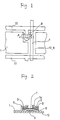
- Figures 1 and 2 show an example of a TFT fabricated by a method of the present invention.
- Figure 1 is a plan view of the TFT
- Figure 2 is a cross-sectional view of the TFT taken along a line A-A' of Figure 1.
- a gate electrode 9 branched from a gate bus line 10 and an intrinsic silicon thin film layer 7 (hereinafter, referred to as an "i layer") are formed on a base substrate 12 made of a glass plate or the like, sandwiching a gate insulating film 8 therebetween.
- a source electrode 2 and a drain electrode 3 are formed on the n + layers 5 and 6, respectively.
- a source auxiliary electrode 1a is formed on the source electrode 2 and connected to a source bus line 4. Further, the drain electrode 3 is connected to a pixel electrode 1.
- the TFT as mentioned above can be fabricated as follows:
- a metal thin film or the like is deposited on the base substrate 12 and etched into a desired configuration and size to form the gate bus line 10 and the gate electrode 9.
- the gate insulating film 8 is formed on the substrate by a CVD method or the like.
- an intrinsic silicon is deposited on the gate insulating film 8 by the plasma CVD method (hereinafter, referred to as the "PCVD method") to form the i layer 7.
- silicon doped with n type impurities is deposited on the i layer 7 by the PCVD method or the like to form an n + layer which will be divided into the n + layers 5 and 6.
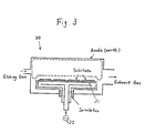
- a dry etching apparatus 20 of a parallel flat plate type in a RIE (Reactive Ion Etching) mode substrates each having the i layer and the n+ layer deposited thereon in the above-mentioned manner are provided on a susceptor 21.
- HCI hydrogen chloride gas
- CF 4 freon-14 gas
- oxygen gas (0 2 ) with the flow ratio (Viz. the ratio of the concentration (mol%) in the apparatus 20) of 5:15:2
- Silicons of the ilayer and the n + layer react with a reaction species generated in this way to form volatile substances, and then the layers are patterned.
- the i layer has a higher activation energy than the n + layer, so that the i layer is less likely to react with the reaction species. Accordingly, it is possible to selectively etch the n + layer.
- the i layer can be patterned as a different step before or after the selective etching.
- phosphorus may be diffused and an active layer may be formed depending on the temperature at the formation of the n + layer on the i layer 7 or the thermal hysteresis in other steps.
- overetching can be used.
- the source electrode 2 and the drain electrode 3 are formed on the n + layers 5 and 6, respectively. Then, a source auxiliary electrode la is formed on the source electrode 2 and connected to the source bus 4, and the pixel electrode 1 is connected to the drain electrode 3. Further, a liquid crystal orientation film is entirely formed on the substrate and liquid crystal is sealed between the substrate and a counter substrate, thereby obtaining a liquid crystal display device.
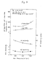
- Figure 4 shows the results obtained by measuring the dependence of the n + /i selectivity, the uniformity of the etch rate of the n + layer (n + uniformity), the etch rates of the n + layer (n + etch rate) and the i layer (i etch rate), upon the gas pressure, in the case where the i layer and the n + layer having the activation energy of 0.2 eV are etched by using an etching gas including hydrogen chloride gas, freon-14 gas and oxygen gas with the flow ratio of 5:15:2 at a stable RF electrical density of 0.25 W/cm 2 .
- an etching gas including hydrogen chloride gas, freon-14 gas and oxygen gas with the flow ratio of 5:15:2 at a stable RF electrical density of 0.25 W/cm 2 .
- n + /i selectivity of a process is a measure of the etch rate of the layer to be etched (n + layer) relative to other material (i layer) on the wafer surface.
- the uniformity of the etch rate of the n + layer is decreased (improved) as the gas pressure raises. Further, when the gas pressure is at 400 m Torr or more, the etch rate of the n + layer sharply increases compared with that of the i layer. When the gas pressure is at 400 m Torr, the n + /i selectivity becomes minimum.
- the n + /i selectivity, and the uniformity of the etch rate of the n + layer can be simultaneously improved when the gas pressure is at 400 m Torr or more.
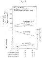
- Figure 5 shows the results obtained by measuring the dependence of the n + /i selectivity, the uniformity of etch rate of the n + layer, and the etch rates of the n + layer and the i layer, upon the gas concentration of freon-14, in the case where the i layer and the n + layer having an activation energy of 0.2 eV are etched at a stable gas pressure of the etching gas of 300 m Torr and a stable RF electrical density of 0.25 W/cm 2 .
- the dependence are measured by varying the flow ratio X of freon-14 in an etching gas including hydrogen chloride gas, freon-14 gas, and oxygen gas with the flow ratio of 5:X:2.
- CF 4 /CF 4 +HCI+0 2 in this diagram represents the flow ratio (Viz. concentration (mol%)) of freon-14 gas against the gross volume of hydrogen chloride gas, freon-14 gas, and oxygen gas
- CF 4 /CF 4 +HCI represents the flow ratio offreon-14 gas against the gross volume of hydrogen chloride gas and freon-14 gas
- 0 2 /CF 4 +HCI+0 2 represents the flow ratio of oxygen gas against the gross volume of hydrogen chloride gas, freon-14 gas, and oxygen gas, respectively.
- the uniformity of the etch rate of the n + layer is decreased (improved) as the concentration (mol%) of freon-14 gas is increased and the concentration of oxygen gas is decreased. Further, the n + /i selectivity is small when the flow ratio X of freon-14 gas is 5; and the n + /i selectivity is increased when X is more than 5 and less than 10; and the n + /i selectivity is almost stable when X is 10 or more.
- the concentration (mol%) of freon-14 gas against the gross volume of hydrogen chloride gas and freon-14 gas is 67% or more, the n + /i selectivity and the uniformity of the etch rate of the n + layer can be simultaneously improved.
- the concentration (mol%) offreon-14 gas against the gross volume of hydrogen chloride, freon-14 gas, and oxygen gas is 58% or more, the n + /i selectivity and the uniformity of the etch rate of the n + layer can be simultaneously improved.
- the concentration (mol%) of oxygen gas in the etching gas is 12% or less, the n + /i selectivity and the uniformity of the etch rate of the n + layer can be simultaneously improved.
- Figure 6 shows the dependence of n + /i selectivity, the n + uniformity, and the etch rates of the n + layer and i layer, upon the gas pressure under the same measurement conditions as those of Figure 4, except that an n + layer having an activation energy of 0.1 eV is used.
- the dependence represent the same tendencies as those of a case where the n + layer having an activation energy of 0.2 eV is used.
- the etch rate of the n + layer has a value almost twice as large as that of such a case.
- the n + /i selectivity is almost doubly improved.
- Etching is promoted in the n + layer having an activation energy of 0.1 eV because electrons of reacting molecules (radical) and those of silicon are exchanged. Accordingly, the etching is smoothly conducted and the etch rate is increased, thereby obtaining the excellent selectivity.
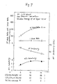
- Figure 7 shows the dependence of n + /i selectivity, the n + uniformity, and the etch rates of the n + layer and i layer, on the concentration (mol%) of freon-14 gas under the same measurement conditions as those of Figure 5, excepting that an n + layer having an activation energy of 0.1 eV is used.
- the dependence represent the same tendencies as those of the case where the n + layer having an activation energy of 0.2 eV is used.
- the n + /i selectivity has further improved compared with that case.
- etching characteristics can be obtained by using a silicon thin film having an activation energy of 0.2 eV or less for the n + layer.
- the i layer 7 is deposited on the substrate with a thickness of 500 angstroms and the n + layer having an activation energy of 0.2 eV is deposited thereon with a thickness of 500 angstroms.
- An etching gas including hydrogen chloride gas, freon-14 gas and oxygen gas having the flow ratio of 5:15:2 and a pressure of 400 m Torr is made to flow into the dry etching apparatus.
- the RF electrical density is set at 0.25 W/cm 2 .
- the etch rate of the n + layer is 250 angstroms/min under the above-mentioned conditions.
- the n + layer should be etched for about 2 minutes.
- etching is conducted for about 3 minutes in order to remove the active layer formed in the i layer by the diffusion of phosphorus included in the n + layer, resulting in a 150% etching of an appropriate etching.
- the n + /i selectivity becomes 2, and the layers can be selectively etched.
- the i layer 7 having a thickness of 300 angstroms is formed without remaining partially undivided on the n + layer nor being excessively etched.
- the n + layers 5 and 6 are excellent in uniformity.
- a liquid crystal display device having an excellent display characteristics can be fabricated by using the TFT formed in this manner.
- the TFT having the same structure as mentioned above is fabricated with an n + layer made of crystallite silicon having an activation energy of 0.1 eV.
- the etch rate becomes 500 angstroms/min under the above-mentioned conditions, so that only 1 minute of etching is required to divide the n + layer into the drain region 5 and the source region 6.
- a 150% etching is conducted in order to remove the active layer formed in the i layer by the diffusion of phosphorus included in the n + layer. Under the above-mentioned conditions, the n + /i selectivity becomes 4, and the layers can be selectively etched.
- the i layer 7 having a thickness of 200 angstroms is formed without remaining partially undivided on the n + layer nor being excessively etched. Further, the n + layers 5 and 6 are excellent in uniformity.
- the liquid crystal display device having an excellent display characteristics can be fabricated by using the TFT formed in this manner.
- a mixed gas of hydrogen chloride gas and freon-14 gas added with oxygen gas is used for the etching.
- the etching gas used for the present invention is not limited to such a mixed gas and the same effect can be obtained with a mixed gas including chlorine gas instead of hydrogen chloride gas.
- a cylindrical apparatus can be used as a dry etching apparatus for the present invention.
- RIE Reactive Ion Etching
- PE Plasma Etching
- ECR mode electrochemical etching
- the dry etching method of the present invention can be applied to a TFT in which an a-SiC:H layer or an a-SiN:H layer is used as an n type silicon layer.
- the n + layerand the i layer having an satisfactory controllability of etching and an uniform etch rate can be selectively etched by the dry etching method using an etching gas including hydrogen chloride gas and freon-14 gas free from the freon regulation.
- a TFT having an i layer of a thin film thickness can be fabricated by taking an advantage of the above-mentioned characteristics of the present invention, so that the optical pumping current can be reduced when the TFT is turned off.
- the distortion of the threshold voltage generated when the optical pumping current is introduced into a gate insulating film can be restrained, so that a liquid crystal display device having excellent display capacities can be obtained.
Landscapes
- Drying Of Semiconductors (AREA)
- Liquid Crystal (AREA)
- Thin Film Transistor (AREA)
Applications Claiming Priority (3)
| Application Number | Priority Date | Filing Date | Title |
|---|---|---|---|
| JP321023/92 | 1992-11-30 | ||
| JP32102392A JP3009975B2 (ja) | 1992-11-30 | 1992-11-30 | シリコン薄膜のドライエッチング方法 |
| JP32102392 | 1992-11-30 |
Publications (3)
| Publication Number | Publication Date |
|---|---|
| EP0600664A2 true EP0600664A2 (fr) | 1994-06-08 |
| EP0600664A3 EP0600664A3 (fr) | 1994-11-23 |
| EP0600664B1 EP0600664B1 (fr) | 2001-05-23 |
Family
ID=18127935
Family Applications (1)
| Application Number | Title | Priority Date | Filing Date |
|---|---|---|---|
| EP93309400A Expired - Lifetime EP0600664B1 (fr) | 1992-11-30 | 1993-11-25 | Procédé d'attaque sèche pour une couche mince de silicium |
Country Status (4)
| Country | Link |
|---|---|
| US (2) | US5783494A (fr) |
| EP (1) | EP0600664B1 (fr) |
| JP (1) | JP3009975B2 (fr) |
| DE (1) | DE69330241T2 (fr) |
Cited By (2)
| Publication number | Priority date | Publication date | Assignee | Title |
|---|---|---|---|---|
| WO2002097852A3 (fr) * | 2001-03-30 | 2003-04-03 | Lam Res Corp | Gravure par plasma de carbure de silicium |
| US7084070B1 (en) | 2001-03-30 | 2006-08-01 | Lam Research Corporation | Treatment for corrosion in substrate processing |
Families Citing this family (7)
| Publication number | Priority date | Publication date | Assignee | Title |
|---|---|---|---|---|
| JPH07263415A (ja) * | 1994-03-18 | 1995-10-13 | Fujitsu Ltd | 半導体装置の製造方法 |
| US6284576B1 (en) * | 1996-07-04 | 2001-09-04 | Sharp Kabushiki Kaisha | Manufacturing method of a thin-film transistor of a reverse staggered type |
| TW463300B (en) * | 1998-08-07 | 2001-11-11 | United Microelectronics Corp | Manufacturing method of self-aligned via for preventing the poisoning of the via |
| FR2890236B1 (fr) * | 2005-08-30 | 2007-11-30 | Commissariat Energie Atomique | Procede de fabrication de circuits en couches minces en silicium amorphe et polycristallin |
| US9515089B1 (en) | 2015-05-14 | 2016-12-06 | International Business Machines Corporation | Bulk fin formation with vertical fin sidewall profile |
| US9627263B1 (en) | 2015-11-30 | 2017-04-18 | International Business Machines Corporation | Stop layer through ion implantation for etch stop |
| US9887135B1 (en) | 2017-04-28 | 2018-02-06 | Globalfoundries Inc. | Methods for providing variable feature widths in a self-aligned spacer-mask patterning process |
Family Cites Families (14)
| Publication number | Priority date | Publication date | Assignee | Title |
|---|---|---|---|---|
| US101302A (en) * | 1870-03-29 | Improvement in tie-bar for holding bent wood | ||
| US4383885A (en) * | 1980-02-06 | 1983-05-17 | Bell Telephone Laboratories, Incorporated | Reactive sputter etching of polysilicon utilizing a chlorine etch gas |
| UST101302I4 (en) * | 1980-03-17 | 1981-12-01 | Selective reactive ion etching of polycrystalline silicon against monocrystalline silicon | |
| JPS56144542A (en) * | 1980-03-17 | 1981-11-10 | Ibm | Method of selectively reactively ion etching polycrystalline silicon for monocrsytalline silicon |
| JPS57174466A (en) * | 1981-04-22 | 1982-10-27 | Hitachi Ltd | Dry etching method |
| US4490209B2 (en) * | 1983-12-27 | 2000-12-19 | Texas Instruments Inc | Plasma etching using hydrogen bromide addition |
| US4789426A (en) * | 1987-01-06 | 1988-12-06 | Harris Corp. | Process for performing variable selectivity polysilicon etch |
| US4799991A (en) * | 1987-11-02 | 1989-01-24 | Motorola, Inc. | Process for preferentially etching polycrystalline silicon |
| US5543646A (en) * | 1988-09-08 | 1996-08-06 | Mitsubishi Denki Kabushiki Kaisha | Field effect transistor with a shaped gate electrode |
| US4992134A (en) * | 1989-11-14 | 1991-02-12 | Advanced Micro Devices, Inc. | Dopant-independent polysilicon plasma etch |
| JPH03270223A (ja) * | 1990-03-20 | 1991-12-02 | Sharp Corp | 非晶質シリコン薄膜のドライエッチング方法 |
| JPH047822A (ja) * | 1990-04-25 | 1992-01-13 | Fuji Xerox Co Ltd | 半導体装置の製造方法 |
| EP0504390B1 (fr) * | 1990-10-05 | 1996-01-10 | General Electric Company | Structure de transistor a film mince avec contacts ameliores source/drain |
| US5384009A (en) * | 1993-06-16 | 1995-01-24 | Applied Materials, Inc. | Plasma etching using xenon |
-
1992
- 1992-11-30 JP JP32102392A patent/JP3009975B2/ja not_active Expired - Lifetime
-
1993
- 1993-11-25 EP EP93309400A patent/EP0600664B1/fr not_active Expired - Lifetime
- 1993-11-25 DE DE69330241T patent/DE69330241T2/de not_active Expired - Lifetime
-
1995
- 1995-09-07 US US08/524,886 patent/US5783494A/en not_active Expired - Lifetime
-
1998
- 1998-07-21 US US09/119,993 patent/US6133157A/en not_active Expired - Lifetime
Cited By (4)
| Publication number | Priority date | Publication date | Assignee | Title |
|---|---|---|---|---|
| WO2002097852A3 (fr) * | 2001-03-30 | 2003-04-03 | Lam Res Corp | Gravure par plasma de carbure de silicium |
| US6919278B2 (en) | 2001-03-30 | 2005-07-19 | Lam Research Corporation | Method for etching silicon carbide |
| US7084070B1 (en) | 2001-03-30 | 2006-08-01 | Lam Research Corporation | Treatment for corrosion in substrate processing |
| US7166535B2 (en) | 2001-03-30 | 2007-01-23 | Lam Research Corporation | Plasma etching of silicon carbide |
Also Published As
| Publication number | Publication date |
|---|---|
| DE69330241T2 (de) | 2001-10-18 |
| EP0600664A3 (fr) | 1994-11-23 |
| EP0600664B1 (fr) | 2001-05-23 |
| US5783494A (en) | 1998-07-21 |
| US6133157A (en) | 2000-10-17 |
| JPH06168915A (ja) | 1994-06-14 |
| JP3009975B2 (ja) | 2000-02-14 |
| DE69330241D1 (de) | 2001-06-28 |
Similar Documents
| Publication | Publication Date | Title |
|---|---|---|
| US5286344A (en) | Process for selectively etching a layer of silicon dioxide on an underlying stop layer of silicon nitride | |
| CA1160761A (fr) | Fabrication de dispositifs microminiaturises par gravure au plasma sur silicone, et produit ainsi obtenu | |
| US4436584A (en) | Anisotropic plasma etching of semiconductors | |
| JPH0744175B2 (ja) | エッチング方法 | |
| US5798303A (en) | Etching method for use in fabrication of semiconductor devices | |
| KR100580782B1 (ko) | 인듐 및 주석 산화물의 건식 에칭 방법 | |
| US5783494A (en) | Selective dry etching method of undoped and doped silicon thin films | |
| US5856239A (en) | Tungsten silicide/ tungsten polycide anisotropic dry etch process | |
| US5700699A (en) | Method for fabricating a polycrystal silicon thin film transistor | |
| US7214979B2 (en) | Selectively deposited silicon oxide layers on a silicon substrate | |
| US5258095A (en) | Method for producing a device having an insulator sandwiched between two semiconductor layers | |
| US4479850A (en) | Method for etching integrated semiconductor circuits containing double layers consisting of polysilicon and metal silicide | |
| US6399515B1 (en) | Plasma etch method for forming patterned chlorine containing plasma etchable silicon containing layer with enhanced sidewall profile uniformity | |
| JP2000252259A (ja) | ドライエッチング方法及び半導体装置の製造方法 | |
| EP0050973B1 (fr) | Procédé de masquage pour dispositif semiconducteurs utilisant une couche de polymère | |
| US4566941A (en) | Reactive ion etching method | |
| US5908791A (en) | Method of forming a polycide gate of a semiconductor device | |
| JPH09512667A (ja) | 薄膜半導体部品の側面をパッシベーション処理する方法 | |
| KR970003886B1 (ko) | 실리콘박막의 건식에칭방법 | |
| JP2939783B2 (ja) | 薄膜トランジスタの製造方法 | |
| KR20020058450A (ko) | 습식방법에 의한 실리콘의 선택적 식각 방법 | |
| JP2739228B2 (ja) | 半導体デバイスの製造方法 | |
| US6191016B1 (en) | Method of patterning a layer for a gate electrode of a MOS transistor | |
| JP2692914B2 (ja) | 薄膜トランジスタの製造方法 | |
| EP0379208B1 (fr) | Procédé pour produire un dispositif ayant une couche isolante prise en sandwich entre deux couches semi-conductrices |
Legal Events
| Date | Code | Title | Description |
|---|---|---|---|
| PUAI | Public reference made under article 153(3) epc to a published international application that has entered the european phase |
Free format text: ORIGINAL CODE: 0009012 |
|
| AK | Designated contracting states |
Kind code of ref document: A2 Designated state(s): DE FR GB |
|
| PUAL | Search report despatched |
Free format text: ORIGINAL CODE: 0009013 |
|
| AK | Designated contracting states |
Kind code of ref document: A3 Designated state(s): DE FR GB |
|
| 17P | Request for examination filed |
Effective date: 19950127 |
|
| 17Q | First examination report despatched |
Effective date: 19950329 |
|
| GRAG | Despatch of communication of intention to grant |
Free format text: ORIGINAL CODE: EPIDOS AGRA |
|
| GRAG | Despatch of communication of intention to grant |
Free format text: ORIGINAL CODE: EPIDOS AGRA |
|
| GRAG | Despatch of communication of intention to grant |
Free format text: ORIGINAL CODE: EPIDOS AGRA |
|
| GRAH | Despatch of communication of intention to grant a patent |
Free format text: ORIGINAL CODE: EPIDOS IGRA |
|
| GRAG | Despatch of communication of intention to grant |
Free format text: ORIGINAL CODE: EPIDOS AGRA |
|
| GRAH | Despatch of communication of intention to grant a patent |
Free format text: ORIGINAL CODE: EPIDOS IGRA |
|
| GRAA | (expected) grant |
Free format text: ORIGINAL CODE: 0009210 |
|
| AK | Designated contracting states |
Kind code of ref document: B1 Designated state(s): DE FR GB |
|
| REF | Corresponds to: |
Ref document number: 69330241 Country of ref document: DE Date of ref document: 20010628 |
|
| ET | Fr: translation filed | ||
| REG | Reference to a national code |
Ref country code: GB Ref legal event code: IF02 |
|
| PLBE | No opposition filed within time limit |
Free format text: ORIGINAL CODE: 0009261 |
|
| 26N | No opposition filed | ||
| PGFP | Annual fee paid to national office [announced via postgrant information from national office to epo] |
Ref country code: DE Payment date: 20121121 Year of fee payment: 20 Ref country code: FR Payment date: 20121130 Year of fee payment: 20 |
|
| PGFP | Annual fee paid to national office [announced via postgrant information from national office to epo] |
Ref country code: GB Payment date: 20121121 Year of fee payment: 20 |
|
| REG | Reference to a national code |
Ref country code: DE Ref legal event code: R071 Ref document number: 69330241 Country of ref document: DE |
|
| REG | Reference to a national code |
Ref country code: GB Ref legal event code: PE20 Expiry date: 20131124 |
|
| PG25 | Lapsed in a contracting state [announced via postgrant information from national office to epo] |
Ref country code: GB Free format text: LAPSE BECAUSE OF EXPIRATION OF PROTECTION Effective date: 20131124 Ref country code: DE Free format text: LAPSE BECAUSE OF EXPIRATION OF PROTECTION Effective date: 20131126 |