EP0602058B1 - Color synthesizing scanning electron microscope - Google Patents
Color synthesizing scanning electron microscope Download PDFInfo
- Publication number
- EP0602058B1 EP0602058B1 EP92916653A EP92916653A EP0602058B1 EP 0602058 B1 EP0602058 B1 EP 0602058B1 EP 92916653 A EP92916653 A EP 92916653A EP 92916653 A EP92916653 A EP 92916653A EP 0602058 B1 EP0602058 B1 EP 0602058B1
- Authority
- EP
- European Patent Office
- Prior art keywords
- signals
- color
- electron microscope
- scanning electron
- specimen
- Prior art date
- Legal status (The legal status is an assumption and is not a legal conclusion. Google has not performed a legal analysis and makes no representation as to the accuracy of the status listed.)
- Expired - Lifetime
Links
Images


Classifications
-
- H—ELECTRICITY
- H01—ELECTRIC ELEMENTS
- H01J—ELECTRIC DISCHARGE TUBES OR DISCHARGE LAMPS
- H01J37/00—Discharge tubes with provision for introducing objects or material to be exposed to the discharge, e.g. for the purpose of examination or processing thereof
- H01J37/02—Details
- H01J37/22—Optical, image processing or photographic arrangements associated with the tube
- H01J37/222—Image processing arrangements associated with the tube
-
- H—ELECTRICITY
- H01—ELECTRIC ELEMENTS
- H01J—ELECTRIC DISCHARGE TUBES OR DISCHARGE LAMPS
- H01J37/00—Discharge tubes with provision for introducing objects or material to be exposed to the discharge, e.g. for the purpose of examination or processing thereof
- H01J37/26—Electron or ion microscopes; Electron or ion diffraction tubes
- H01J37/28—Electron or ion microscopes; Electron or ion diffraction tubes with scanning beams
-
- H—ELECTRICITY
- H01—ELECTRIC ELEMENTS
- H01J—ELECTRIC DISCHARGE TUBES OR DISCHARGE LAMPS
- H01J2237/00—Discharge tubes exposing object to beam, e.g. for analysis treatment, etching, imaging
- H01J2237/244—Detection characterized by the detecting means
- H01J2237/2448—Secondary particle detectors
-
- H—ELECTRICITY
- H01—ELECTRIC ELEMENTS
- H01J—ELECTRIC DISCHARGE TUBES OR DISCHARGE LAMPS
- H01J2237/00—Discharge tubes exposing object to beam, e.g. for analysis treatment, etching, imaging
- H01J2237/244—Detection characterized by the detecting means
- H01J2237/24495—Signal processing, e.g. mixing of two or more signals
Definitions
- the present invention relates generally to the field of scanning electron microscopes (SEM). More specifically, the present invention relates to a color synthesizing scanning electron microscope configured to produce color images of high information content by arranging at least two wide energy bandwidth secondary detectors around a specimen, to detect electrons with trajectory or positional differences.
- SEM scanning electron microscopes
- Scanning electron microscopes are commonly used for observation and analysis of matter. Scanning electron microscopes have found broad application in the transistor industry to show voltage distribution in such devices. Other uses include industrial quality control and a broad range of industrial and biological research.
- a scanning electron microscope typically includes a vacuum chamber, an electron optical system for generating and focusing an electron beam (referred to also as the primary electron beam) at a specimen , a deflection system for moving the beam across a specimen in a predetermined raster pattern, a detector system for detecting phenomena from the specimen caused by the impinging primary electron beam, and a display system.
- an electron optical system for generating and focusing an electron beam (referred to also as the primary electron beam) at a specimen
- a deflection system for moving the beam across a specimen in a predetermined raster pattern
- a detector system for detecting phenomena from the specimen caused by the impinging primary electron beam
- the short-lived phenomena include secondary electrons (low energy), back-scattered electrons (high energy), x-ray characteristics of the specimen, "white x-rays", light (cathode luminescence), absorbed electrons, transmitted electrons, and auger process electrons (low energy). Detectors for each of the above phenomena are well known in the art.
- a conventional scanning electron microscope typically at least one of the signals identified above is detected, amplified and displayed on a CRT (cathode ray tube).
- the amplitude of the signal is used to modulate the intensity of the beam of the CRT.
- the beam of the CRT is deflected in a raster pattern which corresponds to and is synchronized with the scanning primary electron beam of the SEM.
- a black and white image of the specimen is thereby presented to the operator of the microscope.
- the image thus created may be set to contain three types of information at each point on the CRT, two position vectors which identify the location of the primary electron beam on the specimen, and one brightness or intensity level vector which contains information about the specimen.
- the intensity level is usually derived from the secondary electron emission, which contains topographical (slope) information.
- the information thus presented is in a form which is readily accepted by the human operator who can rapidly assimilate the information.
- One or more of the many signals which are induced by the primary electron beam can be displayed in a conventional scanning electron microscope system at any one time.
- Each of the various responses of the specimen to the primary electron beam includes unique information about the specimen.
- the intensity of the secondary electron emission contains information about the slope of the specimen surface, with respect to the primary electron beam. This information can be used to generate an image of the specimen surface.
- the back-scattered (high energy) electron signal contains information about the atomic number of the specimen, and thus can be used to provide a profile having an intensity which is representative of the chemical makeup rather than the shape of the specimen under examination. In a conventional scanning electron microscope with display, the operator can observe any one or more than one of these images at a time.
- Color synthesizers have been proposed in the prior art to enhance the display image of scanning electron microscopes. For the most part, these color imaging schemes have not increased the information content of the image but have been utilized merely to present a more aesthetically pleasing picture.
- Color pictures have been produced photographically by means of multiple exposures of film through appropriately colored filters.
- One prior system utilizes three separate x-rays, each representative of a different element, which are used to modulate the three electron guns of a color kinescope. That is, each x-ray detector is associated with a different color and these elements are then displayed concurrently and in color. The resultant image defines the distribution of the elements in the specimen since each one is represented by a different color.
- colored images are constructed in which different regions of the image are colored in accordance with a color coding scheme, in such a fashion that variations in a physical variable are represented by different colors in the image. While such colored images convey information in a fashion which can be readily assimilated, the information content is generally no greater than would be conveyed had the colors not been used and the image simply coded monochromatically such as by different shading patterns. This is in contrast to the images normally perceived by the eye where, because of the added mixed light impressions perceived, a variety of lighting effects can be differentiated, which impressions can hardly be adequately represented monochromatically. This arises because a colored image as perceived by the eye can be considered as being made up of three simultaneously perceived images, each of a separate primary color, and the eye is capable of differentiating regions in the image as to which of the relative proportions of the three primary colors vary.
- U.S. Patent Nos. 3,628,014, 4,041,311, 4,560,872 and 5,001,344 propose techniques which generate color images from the information available in a scanning electron microscope and display the images on a color CRT.
- the images are continuous in hue and cover the entire color range.
- Such techniques generate color images in real time as distinguished from photographic images.
- these techniques are not useful for producing color images at the low voltages typically used during examination of biological specimens.
- the images produced, although satisfactory, do not provide a substantial amount of information about the specimen.
- the present invention is directed to a color synthesizing scanning electron microscope which produces color images of high information content, which are more easily interpreted and graphically presented than images obtained by prior systems.
- a color synthesizing scanning electron microscope according to the present invention is defined in claim 1.
- a method for generating color images with such an electron microscope is defined in claim 15.
- the angles of the detectors vary both laterally around the specimen and vertically.
- the variation in the vertical angle of the detector is a factor in determining the proportion of secondary to other electrons that are detected.
- a differential amplifier generates additional signals for representing a difference between any two input signals from the secondary detectors.
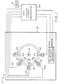
- Figure 1 illustrates generally a color synthesizing scanning electron microscope 10 in accordance with a preferred embodiment of the present invention.
- the color synthesizing SEM 10 produces color images of a specimen 12. The color images provide more information about the specimen than prior systems, which is easily interpreted and more graphically presented.
- the color synthesizing SEM 10 is particularly desirable for examining specimens at low voltages, for example, when the primary electron beam voltage is 5kV (kilovolts) and under. Biological and uncoated specimens are typically examined at low voltages.
- the color synthesizing SEM comprises a scanning electron microscope (SEM) 13, of conventional design. Following well known techniques of the scanning electron microscope 13, the surface of the specimen 12 is bombarded with the primary beam of electrons. The specimen 12 emits secondary electrons that are generated by the action of the primary electron beam. These secondary electrons are collected and amplified by the SEM 13. Since the primary electron beam strikes only one point one the specimen 12, the primary electron beam is scanned over the specimen 12 in a raster pattern to generate pictures of the specimen surface 12 which are displayed on a CRT 15.
- SEM scanning electron microscope
- Major elements of the scanning electron microscope include electromagnetic lenses (not shown) that are used to form the electron probe, the scan coils (not shown) that sweep the primary electron beam over the specimen 12, a detector 14 that collects the secondary electrons, and amplifying means (indicated at block 110 in Figure 2) where the secondary electrons are amplified and fed to the CRT 15 for display.
- a conventional vacuum diffusion pump (not shown) is used since a vacuum is required for operation of the primary electron beam.
- the SEM is configured such that at least two and preferably three secondary detectors 14, 16 and 18, associated with the scanning electron microscope 10 are positioned around the specimen 12 to receive electron emission from the specimen 12 subsequent to incidence of the scanning primary electron beam to produce images of the specimen surface in color.
- the images that are formed are easily interpreted because the surface topography, including the illuminating and shadowing effects on the specimen 12 are similar to large objects as normally perceived by the unaided eye.
- the SEM 13 is connected to a SEM color video processor 20.
- the detectors 14, 16 and 18 are configured in accordance with conventional techniques, having suitable electron voltage potentials applied thereto, to attract the secondary electrons.
- conventional wide energy bandwidth secondary detectors are used, such as Everhart-Thornley secondary detectors with wideband photomultiplier tubes and electronics.
- a variable bias ranging between 0 to 300V (volts) is used for the Faraday cage of the detectors 14, 16 and 18 in order to appropriately distribute the available signal electrons, thus optimizing signal to noise ratio for each detector.
- other wideband secondary detectors such as the micro-channel plate type, can be used.
- the detectors 14, 16 and 18 are arranged around the specimen 12, at a suitable angle to detect electrons with trajectory or positional differences.
- the angles at which each of the detectors 14, 16 and 18 is arranged can vary both laterally and vertically.
- the variation in the vertical angle of the detectors 14, 16 and 18 determine the proportion of secondary to other electrons that are detected.
- the central detector 16 is oriented upwards, at a suitable angle from the perpendicular (as shown in Figure 1A) for example 30°, and the detectors 14 and 18 are oriented such that they aim directly at the specimen 12 in order to detect more side-scattered electrons.
- More than three detectors with associated input amplifiers, differential amplifiers and RGB mixers can be used.
- the detectors can be arranged in an arc or a full circle to entirely surround the specimen 12.
- Each of the detectors can be turned on or off, as desired, to experiment with various signals for the purpose of image analysis and to adjust "illumination" (chiaroscuro) by the electrons for recording purposes.
- a back-scatter detector either solid state, scintillator or micro channel plate (MCP) can also be used to detect back-scattered electrons. If a back-scatter detector is used, a relatively high accelerating beam voltage of 10kV or 20kV and above is desired.
- FIG. 2 is a block diagram of the color video processor 20 of the color synthesizing SEM 10 of the present invention.
- the color video processor 20 can be used in applications other than in secondary electron microscopes to derive color signals from three black and white signals.
- Channels 102, 104 and 106 from each of the wide energy bandwidth secondary detectors 14, 16 and 18, respectively, are connected to an input amplifier 110.
- the input amplifier 110 comprises three separate input amplifier stages, a first amplifier stage 112 connected to a channel 102, a second amplifier stage 114 connected to a second channel 104 and a third amplifier stage 116 connected to a third channel 106.
- the amplifier stages 112, 114 and 116 buffer and amplify the channels 102, 104 and 106, respectively, if necessary.
- the outputs of the amplifier stages 112, 114 and 116 are connected to a differential amplifier stage 150.
- the differential amplifier stage 150 generates additional signals at the outputs of the amplifier stages 112, 114 and 116.
- the differential amplifier stage 150 generates signals representative of the difference between any two of the signals at the outputs of the amplifier stages 112, 114 or 116. This stage is particularly useful for producing a third signal in situations where only two wide energy bandwidth secondary detectors are used. In situations where more than two secondary detectors are used, any number of difference signals may be generated by adding a differential amplifier for each desired difference signal.
- the color mixer 200 mixes those signals and produces three outputs 202, 204 and 206, each representative of the colors red, green and blue, respectively.
- the outputs 202, 204 and 206 from the color mixer 200 are connected to an RGB amplifier stage 250.
- the RGB amplifier stage 250 amplifies each of the red, green and blue signals at the outputs 202, 204 and 206 from the color mixer 200.
- the RGB amplifier stage 250 may be adjusted to vary the amount of signal going to each of the output color channels 252, 254 and 256.
- the output channels 252, 254 and 256 from the RGB amplifier stage 250 are preferably connected to a sync and blanking stage 300 which adds the appropriate video blanking and sync signals, which are in synchronization with the scanning primary beam of the color synthesizing SEM 10 of the present invention.
- the sync and blanking stage 300 produces red, green and blue channels 302, 304 and 306, respectively, and a channel monitor signal 308.
- the red, green and blue channels are video signals and the channel monitor signal 308 is a NTSC composite video signal that enables the operator to monitor the signal and corresponding image of any of channels 112, 114, 116 or 152 in black and white, independent of the color output. This signal may as well be simultaneously noise reduced, transcoded and recorded.
- the output channels 252, 254 and 256 can be connected to a film recorder, A/D converters, computer or the like.
- the output channels 302, 304, 306 and 308 may be then connected to any suitable video equipment for viewing the image produced by the color synthesizing SEM 10.
- the output channels 302, 304, 306 and 308 may be connected to a frame averager 350, of conventional design known to those skilled in the art, for noise reduction.
- the frame averager 350 produces red, green, blue, and sync output channels 352, 354, 356 and 358.
- the output channels 352, 354, 356 and 358 from the frame averager 350 may be optionally connected to a video transcoder 400, of conventional design known to those skilled in the art.
- the video transcoder 400 produces composite, Y/C (S-VHS), component or other sync output channels 402, 404, 406 and 408, respectively, for connection to appropriate video equipment.
- Figure 3 is a schematic representation of the an exemplary input amplifier stage 110 of the color video processor 20.
- the secondary detector channels 102, 104 and 106 are connected to the input amplifier stages 112, 114 and 116, respectively, as shown in Figure 2.
- the input amplifier stages 112, 114 and 116 are substantially identical and are represented by the circuit diagram shown in Figure 3.
- the input amplifier stage 112 has resistors R1, R2, R3, R4, R5, R6, R7, R8 and R9, having exemplary resistance values of 150 ⁇ (ohms), 75 ⁇ , 250 ⁇ , 250 ⁇ , 20 ⁇ , 390 ⁇ , 560 ⁇ , 75 ⁇ and 75 ⁇ , respectively.
- the input amplifier stage 112 has capacitors C1 and C2, having exemplary capacitance values of 10 ⁇ F (microfarads) and 3pF (picofarads), respectively.
- the input amplifier stage 112 has an operational amplifier U1, having exemplary part number 621 manufactured by Burr-Brown, and a buffer amplifier U2 to monitor the channels, having exemplary part number 2001 manufactured by Elantec.
- a three pole, double throw switch S1 connects or disconnects the input amplifier 112 from an output channel 122 which is connected to the differential amplifier stage 150 (shown in Figure 2).
- a pole 126 of the switch 124 is connected to a voltage of preferably 3V.
- the switch 124 is in a connected position, as shown in Figure 3, the pole 126 is connected to an indicator lamp 128, indicating that the output of the amplifier stage 112 is connected to the output channel 122.
- the switch 124 is in a disconnected position, the indicator lamp 128 is disconnected and the output channel 122 is also disconnected from the input amplifier stage 112.
- the output of the resistor R9 of the input amplifier stage 112 is connected to a monitor select switch 310 (shown in Figure 7).
- Figure 4 is a schematic representation of the differential amplifier 152 of the differential amplifier stage 150 and is exemplary of all the differential amplifiers included within the stage 150.
- the differential amplifier 152 has a variable resistor VR1, which has an exemplary resistance value of 1k ⁇ and which is connected to a double pole, double throw switch S2.
- the variable resistor VR1 adjusts the balance between inputs 154 and 156 (also shown in Figure 2).
- the differential amplifier 152 has resistors R10, R11, R12, R13, R14, R15, R16, R17 and R18, having exemplary resistance values of 110 ⁇ , 110 ⁇ , 250 ⁇ , 250 ⁇ , 20 ⁇ , 560 ⁇ , 390 ⁇ , 75 ⁇ and 75 ⁇ , respectively.
- the differential amplifier 152 has an operational amplifier U3 having exemplary part number 620 or 621 manufactured by Burr-Brown and a buffer amplifier U4 having exemplary part number 2001 manufactured by Elantec.
- the output of the resistor R18 is connected to the monitor select switch 310 (shown in Figure 7).
- FIG. 5 is a schematic representation of the color mixer 200 shown for an exemplary configuration of three secondary detector channels 208, 210 and 212, and two differential output channels 214 and 216 from the differential amplifier stage 150.
- Each channel is connected to three variable resistors, each indicated at VR2 and having an exemplary resistance value of 500 ⁇ .
- Each variable resistor VR2 is connected to a resistor R19, R20 and R21, each having exemplary resistance values of 250 ⁇ .
- the resistors R19, R20 and R21 are connected to the red output channel 202, the green output channel 204 and the blue output channel 206, respectively.
- FIG. 6 is a schematic representation of the RGB amplifier 250.
- the RGB amplifier 250 has preferably three amplifiers on a chip having an exemplary part number LM 1203 manufactured by Texas Instruments. Resistors R22, R23, R24, R25 and R26, have exemplary resistance values of 75 ⁇ , 10k ⁇ , 150 ⁇ , 390 ⁇ and 75 ⁇ , respectively.
- the RGB amplifier has a variable resistor VR3 for varying the gain of the red, green and blue outputs, and VR4 for calibrating the gains of each of the red, green and blue output channels 252, 254 and 256, having exemplary resistance values of 10k ⁇ and 100 ⁇ , respectively.
- the RGB amplifier has capacitors C3, C4, C5, C6, C7, C8, C9 and C10, having exemplary capacitance values of 10 ⁇ F (microfarads), 10 ⁇ F, 0.1 ⁇ F, 0.1 ⁇ F, 10 ⁇ F, 0.1 ⁇ F, 0.1 ⁇ F and 100 ⁇ F, respectively.
- the output channels 252, 254 and 256 from the RGB amplifier stage 250 are preferably connected to a sync and blanking stage 300, as shown in Figure 2.
- FIG. 7 is a schematic representation of the sync and blanking stage 300.
- a blanking input 302 is connected to an NPN transistor Q1, having an exemplary part number 2N3904 manufactured by Motorola, and a PNP transistor Q2, having an exemplary part number of 2N3906 manufactured by Motorola.
- Resistors R27, R28, R29, R30 and R31, having exemplary resistance values of 83k ⁇ , 24k ⁇ , 3.6k ⁇ , 24k ⁇ , and 1.8k ⁇ , and diodes D1, having exemplary part number 1N914, are connected to the transistors Q1 and Q2.
- Transistors Q3 and Q4 are coupled between the output 252 from the RGB amplifier 250 and the red output 302 from the sync and blanking pulse adder 300 (shown in Figure 2) and have exemplary part numbers of 2N4239 and 2N5639, respectively.
- Resistors R32, R42, R43, R44, R45 and R46 having exemplary resistance values of 39k ⁇ , 75 ⁇ , 290 ⁇ , 100 ⁇ , 18k ⁇ and 470 ⁇ , respectively, and capacitors C11 and C13, each having an exemplary capacitance value of 100 ⁇ F, are connected to the transistors Q3 and Q4.
- Diode D1 is connected between the transistors Q3 and Q4.
- the circuit connected between the output 254 from the RGB amplifier 250 and the green output 304, the circuit connected between the output 256 from the RGB amplifier 250 and the blue output 306, and the circuit connected between the monitor select switch 310 and a transistor Q5 are all configured in an identical manner with the circuit between the output 252 from the RGB amplifier 250 and the red output 302. Each circuit is shown in Figure 7 within broken lines.
- the transistor Q5 is a PNP transistor having an exemplary part number of 2N3906 manufactured by Motorola.
- Resistors R37, R38, R39 and variable resistor VR7 having exemplary resistance values of 7.5k ⁇ , 27k ⁇ , 100 ⁇ and 5k ⁇ , are connected between the transistor Q5 and a sync input 312.
Landscapes
- Chemical & Material Sciences (AREA)
- Analytical Chemistry (AREA)
- Engineering & Computer Science (AREA)
- Computer Vision & Pattern Recognition (AREA)
- Analysing Materials By The Use Of Radiation (AREA)
- Apparatus For Radiation Diagnosis (AREA)
Applications Claiming Priority (3)
| Application Number | Priority Date | Filing Date | Title |
|---|---|---|---|
| US07/737,942 US5212383A (en) | 1991-07-29 | 1991-07-29 | Color synthesizing scanning electron microscope |
| US737942 | 1991-07-29 | ||
| PCT/US1992/006103 WO1993003491A1 (en) | 1991-07-29 | 1992-07-22 | Color synthesizing scanning electron microscope |
Publications (3)
| Publication Number | Publication Date |
|---|---|
| EP0602058A1 EP0602058A1 (en) | 1994-06-22 |
| EP0602058A4 EP0602058A4 (en) | 1994-09-28 |
| EP0602058B1 true EP0602058B1 (en) | 2002-11-06 |
Family
ID=24965901
Family Applications (1)
| Application Number | Title | Priority Date | Filing Date |
|---|---|---|---|
| EP92916653A Expired - Lifetime EP0602058B1 (en) | 1991-07-29 | 1992-07-22 | Color synthesizing scanning electron microscope |
Country Status (10)
| Country | Link |
|---|---|
| US (1) | US5212383A (cs) |
| EP (1) | EP0602058B1 (cs) |
| JP (1) | JP3270046B2 (cs) |
| KR (1) | KR100246633B1 (cs) |
| AT (1) | ATE227470T1 (cs) |
| AU (1) | AU657995B2 (cs) |
| CA (1) | CA2114020C (cs) |
| CZ (1) | CZ18094A3 (cs) |
| DE (1) | DE69232841T2 (cs) |
| WO (1) | WO1993003491A1 (cs) |
Families Citing this family (10)
| Publication number | Priority date | Publication date | Assignee | Title |
|---|---|---|---|---|
| GB9209500D0 (en) * | 1992-05-01 | 1992-06-17 | Link Analytical Ltd | X-ray analysis apparatus |
| GB2285169A (en) * | 1993-12-21 | 1995-06-28 | Secretary Trade Ind Brit | Scanning electron microscope grain imaging |
| JP3291880B2 (ja) * | 1993-12-28 | 2002-06-17 | 株式会社日立製作所 | 走査形電子顕微鏡 |
| EP0826145B1 (en) * | 1995-05-13 | 2001-08-16 | International Business Machines Corporation | Data acquisition and control apparatus for scanning probe systems |
| US6353222B1 (en) | 1998-09-03 | 2002-03-05 | Applied Materials, Inc. | Determining defect depth and contour information in wafer structures using multiple SEM images |
| US6201240B1 (en) | 1998-11-04 | 2001-03-13 | Applied Materials, Inc. | SEM image enhancement using narrow band detection and color assignment |
| US6627886B1 (en) * | 1999-05-14 | 2003-09-30 | Applied Materials, Inc. | Secondary electron spectroscopy method and system |
| FR2800196B1 (fr) * | 1999-10-21 | 2001-11-23 | Mona Lisa Production | Procede de prise de vues par microscopie electronique et methode de realisation d'un film video sur au moins un animal de faible taille |
| US6930308B1 (en) * | 2002-07-11 | 2005-08-16 | Kla-Tencor Technologies Corporation | SEM profile and surface reconstruction using multiple data sets |
| DE102015116272A1 (de) | 2015-09-25 | 2017-03-30 | Heinrich-Pette-Institut Leibniz-Institut für experimentelle Virologie | Polychromatische Elektronenmikroskopie |
Family Cites Families (14)
| Publication number | Priority date | Publication date | Assignee | Title |
|---|---|---|---|---|
| US3628014A (en) * | 1969-12-22 | 1971-12-14 | Boeing Co | Scanning electron microscope with color display means |
| US3812288A (en) * | 1972-11-21 | 1974-05-21 | Edax Int Inc | Television display system |
| US4068123A (en) * | 1973-07-27 | 1978-01-10 | Nihon Denshi Kabushiki Kaisha | Scanning electron microscope |
| GB1443562A (en) * | 1973-08-14 | 1976-07-21 | Ontario Research Foundation | Method and apparatus for displaying images stereoscopically and for deriving signals from a scanning electron microscope for producing steroscopic images |
| US4041311A (en) * | 1976-07-12 | 1977-08-09 | Iowa State University Research Foundation, Inc. | Scanning electron microscope with color image display |
| US4439680A (en) * | 1980-06-26 | 1984-03-27 | Regents Of The University Of Minnesota | Color-coded mapping system and method for identifying elements in a specimen |
| JPS57126056A (en) * | 1981-01-29 | 1982-08-05 | Akashi Seisakusho Co Ltd | Scanning-type electronic microscope which can display plural sample images simultaneously, and device similar to it |
| JPS58501396A (ja) * | 1981-09-01 | 1983-08-18 | コモンウエルス サイエンテイフイツク アンド インダストリアル リサ−チ オ−ガニゼ−シヨン | 画像形成方法および装置 |
| US4588890A (en) * | 1984-12-31 | 1986-05-13 | International Business Machines Corporation | Apparatus and method for composite image formation by scanning electron beam |
| US4673988A (en) * | 1985-04-22 | 1987-06-16 | E.I. Du Pont De Nemours And Company | Electronic mosaic imaging process |
| GB8622976D0 (en) * | 1986-09-24 | 1986-10-29 | Trialsite Ltd | Scanning electron microscopes |
| US4857731A (en) * | 1987-04-17 | 1989-08-15 | Jeol Ltd. | Instrument for analyzing specimen |
| JPH01102841A (ja) * | 1987-10-14 | 1989-04-20 | Toshiba Corp | 画像形成方法 |
| JP2786207B2 (ja) * | 1988-08-26 | 1998-08-13 | 株式会社日立製作所 | 走査型顕微鏡における表面形状算出方法 |
-
1991
- 1991-07-29 US US07/737,942 patent/US5212383A/en not_active Expired - Lifetime
-
1992
- 1992-07-22 CA CA002114020A patent/CA2114020C/en not_active Expired - Fee Related
- 1992-07-22 JP JP50361493A patent/JP3270046B2/ja not_active Expired - Fee Related
- 1992-07-22 CZ CS94180A patent/CZ18094A3/cs unknown
- 1992-07-22 KR KR1019940700250A patent/KR100246633B1/ko not_active Expired - Fee Related
- 1992-07-22 AT AT92916653T patent/ATE227470T1/de not_active IP Right Cessation
- 1992-07-22 DE DE69232841T patent/DE69232841T2/de not_active Expired - Fee Related
- 1992-07-22 AU AU23838/92A patent/AU657995B2/en not_active Ceased
- 1992-07-22 WO PCT/US1992/006103 patent/WO1993003491A1/en not_active Ceased
- 1992-07-22 EP EP92916653A patent/EP0602058B1/en not_active Expired - Lifetime
Also Published As
| Publication number | Publication date |
|---|---|
| AU657995B2 (en) | 1995-03-30 |
| JP3270046B2 (ja) | 2002-04-02 |
| JPH06509903A (ja) | 1994-11-02 |
| EP0602058A4 (en) | 1994-09-28 |
| DE69232841D1 (de) | 2002-12-12 |
| AU2383892A (en) | 1993-03-02 |
| ATE227470T1 (de) | 2002-11-15 |
| CZ18094A3 (en) | 1994-06-15 |
| CA2114020C (en) | 1999-05-25 |
| WO1993003491A1 (en) | 1993-02-18 |
| CA2114020A1 (en) | 1993-02-18 |
| EP0602058A1 (en) | 1994-06-22 |
| US5212383A (en) | 1993-05-18 |
| DE69232841T2 (de) | 2003-09-18 |
| KR100246633B1 (ko) | 2000-03-15 |
Similar Documents
| Publication | Publication Date | Title |
|---|---|---|
| US4041311A (en) | Scanning electron microscope with color image display | |
| US4211924A (en) | Transmission-type scanning charged-particle beam microscope | |
| EP0602058B1 (en) | Color synthesizing scanning electron microscope | |
| CA2234950A1 (en) | Imaging system | |
| EP0241060B1 (en) | Apparatus for energy-selective visualisation | |
| US5382796A (en) | Apparatus for morphological observation of a sample | |
| US6573502B2 (en) | Combined electron microscope | |
| US3986027A (en) | Stereo scanning microprobe | |
| US3541233A (en) | Color conversion system for x-rays | |
| US4006357A (en) | Apparatus for displaying image of specimen | |
| EP0746946B1 (en) | Display device comprising a cathode ray tube | |
| GB1588234A (en) | Transmission type beam nicroscopes utilising a scanning technique | |
| JP3439508B2 (ja) | 試料画像表示装置 | |
| JPS60138252U (ja) | 粒子線装置における試料画像表示装置 | |
| CN111146062A (zh) | 电子显微镜和图像处理方法 | |
| JPS62198043A (ja) | 立体観察装置 | |
| JP2775812B2 (ja) | 荷電粒子線装置 | |
| KR830002861Y1 (ko) | 주사전자 현미경 및 그의유사장치의 주사상 관찰장치 | |
| JPS63116348A (ja) | 電子線装置の視野対応装置 | |
| JPH0352179B2 (cs) | ||
| JP2751182B2 (ja) | カラー受像管のランディング測定装置及びその測定方法 | |
| CA1052011A (en) | Stero scanning electron microscopy | |
| JPS5827621B2 (ja) | 走査電子顕微鏡 | |
| JPS62222557A (ja) | 立体観察装置 | |
| JPS5857248A (ja) | 走査形電子顕微鏡 |
Legal Events
| Date | Code | Title | Description |
|---|---|---|---|
| PUAI | Public reference made under article 153(3) epc to a published international application that has entered the european phase |
Free format text: ORIGINAL CODE: 0009012 |
|
| 17P | Request for examination filed |
Effective date: 19940121 |
|
| AK | Designated contracting states |
Kind code of ref document: A1 Designated state(s): AT BE CH DE DK ES FR GB GR IT LI LU MC NL SE |
|
| A4 | Supplementary search report drawn up and despatched |
Effective date: 19940808 |
|
| AK | Designated contracting states |
Kind code of ref document: A4 Designated state(s): AT BE CH DE DK ES FR GB GR IT LI LU MC NL SE |
|
| 17Q | First examination report despatched |
Effective date: 19951115 |
|
| GRAG | Despatch of communication of intention to grant |
Free format text: ORIGINAL CODE: EPIDOS AGRA |
|
| GRAG | Despatch of communication of intention to grant |
Free format text: ORIGINAL CODE: EPIDOS AGRA |
|
| GRAH | Despatch of communication of intention to grant a patent |
Free format text: ORIGINAL CODE: EPIDOS IGRA |
|
| GRAH | Despatch of communication of intention to grant a patent |
Free format text: ORIGINAL CODE: EPIDOS IGRA |
|
| GRAA | (expected) grant |
Free format text: ORIGINAL CODE: 0009210 |
|
| AK | Designated contracting states |
Kind code of ref document: B1 Designated state(s): AT BE CH DE DK ES FR GB GR IT LI LU MC NL SE |
|
| PG25 | Lapsed in a contracting state [announced via postgrant information from national office to epo] |
Ref country code: NL Free format text: LAPSE BECAUSE OF FAILURE TO SUBMIT A TRANSLATION OF THE DESCRIPTION OR TO PAY THE FEE WITHIN THE PRESCRIBED TIME-LIMIT Effective date: 20021106 Ref country code: LI Free format text: LAPSE BECAUSE OF FAILURE TO SUBMIT A TRANSLATION OF THE DESCRIPTION OR TO PAY THE FEE WITHIN THE PRESCRIBED TIME-LIMIT Effective date: 20021106 Ref country code: IT Free format text: LAPSE BECAUSE OF FAILURE TO SUBMIT A TRANSLATION OF THE DESCRIPTION OR TO PAY THE FEE WITHIN THE PRESCRIBED TIME-LIMIT;WARNING: LAPSES OF ITALIAN PATENTS WITH EFFECTIVE DATE BEFORE 2007 MAY HAVE OCCURRED AT ANY TIME BEFORE 2007. THE CORRECT EFFECTIVE DATE MAY BE DIFFERENT FROM THE ONE RECORDED. Effective date: 20021106 Ref country code: GR Free format text: LAPSE BECAUSE OF FAILURE TO SUBMIT A TRANSLATION OF THE DESCRIPTION OR TO PAY THE FEE WITHIN THE PRESCRIBED TIME-LIMIT Effective date: 20021106 Ref country code: CH Free format text: LAPSE BECAUSE OF FAILURE TO SUBMIT A TRANSLATION OF THE DESCRIPTION OR TO PAY THE FEE WITHIN THE PRESCRIBED TIME-LIMIT Effective date: 20021106 Ref country code: BE Free format text: LAPSE BECAUSE OF FAILURE TO SUBMIT A TRANSLATION OF THE DESCRIPTION OR TO PAY THE FEE WITHIN THE PRESCRIBED TIME-LIMIT Effective date: 20021106 Ref country code: AT Free format text: LAPSE BECAUSE OF FAILURE TO SUBMIT A TRANSLATION OF THE DESCRIPTION OR TO PAY THE FEE WITHIN THE PRESCRIBED TIME-LIMIT Effective date: 20021106 |
|
| REF | Corresponds to: |
Ref document number: 227470 Country of ref document: AT Date of ref document: 20021115 Kind code of ref document: T |
|
| REG | Reference to a national code |
Ref country code: GB Ref legal event code: FG4D |
|
| REG | Reference to a national code |
Ref country code: CH Ref legal event code: EP |
|
| REF | Corresponds to: |
Ref document number: 69232841 Country of ref document: DE Date of ref document: 20021212 |
|
| PG25 | Lapsed in a contracting state [announced via postgrant information from national office to epo] |
Ref country code: SE Free format text: LAPSE BECAUSE OF FAILURE TO SUBMIT A TRANSLATION OF THE DESCRIPTION OR TO PAY THE FEE WITHIN THE PRESCRIBED TIME-LIMIT Effective date: 20030206 Ref country code: DK Free format text: LAPSE BECAUSE OF FAILURE TO SUBMIT A TRANSLATION OF THE DESCRIPTION OR TO PAY THE FEE WITHIN THE PRESCRIBED TIME-LIMIT Effective date: 20030206 |
|
| NLV1 | Nl: lapsed or annulled due to failure to fulfill the requirements of art. 29p and 29m of the patents act | ||
| REG | Reference to a national code |
Ref country code: CH Ref legal event code: PL |
|
| PG25 | Lapsed in a contracting state [announced via postgrant information from national office to epo] |
Ref country code: ES Free format text: LAPSE BECAUSE OF FAILURE TO SUBMIT A TRANSLATION OF THE DESCRIPTION OR TO PAY THE FEE WITHIN THE PRESCRIBED TIME-LIMIT Effective date: 20030529 |
|
| ET | Fr: translation filed | ||
| PG25 | Lapsed in a contracting state [announced via postgrant information from national office to epo] |
Ref country code: LU Free format text: LAPSE BECAUSE OF NON-PAYMENT OF DUE FEES Effective date: 20030722 |
|
| PG25 | Lapsed in a contracting state [announced via postgrant information from national office to epo] |
Ref country code: MC Free format text: LAPSE BECAUSE OF NON-PAYMENT OF DUE FEES Effective date: 20030731 |
|
| PLBE | No opposition filed within time limit |
Free format text: ORIGINAL CODE: 0009261 |
|
| 26N | No opposition filed |
Effective date: 20030807 |
|
| PGFP | Annual fee paid to national office [announced via postgrant information from national office to epo] |
Ref country code: FR Payment date: 20060725 Year of fee payment: 15 |
|
| PGFP | Annual fee paid to national office [announced via postgrant information from national office to epo] |
Ref country code: DE Payment date: 20070726 Year of fee payment: 16 |
|
| PGFP | Annual fee paid to national office [announced via postgrant information from national office to epo] |
Ref country code: GB Payment date: 20070725 Year of fee payment: 16 |
|
| REG | Reference to a national code |
Ref country code: FR Ref legal event code: ST Effective date: 20080331 |
|
| PG25 | Lapsed in a contracting state [announced via postgrant information from national office to epo] |
Ref country code: FR Free format text: LAPSE BECAUSE OF NON-PAYMENT OF DUE FEES Effective date: 20070731 |
|
| GBPC | Gb: european patent ceased through non-payment of renewal fee |
Effective date: 20080722 |
|
| PG25 | Lapsed in a contracting state [announced via postgrant information from national office to epo] |
Ref country code: DE Free format text: LAPSE BECAUSE OF NON-PAYMENT OF DUE FEES Effective date: 20090203 |
|
| PG25 | Lapsed in a contracting state [announced via postgrant information from national office to epo] |
Ref country code: GB Free format text: LAPSE BECAUSE OF NON-PAYMENT OF DUE FEES Effective date: 20080722 |