EP0602532A2 - Multi-Schicht Struktur mit einer epitaxialer metallischer Elektrode - Google Patents
Multi-Schicht Struktur mit einer epitaxialer metallischer Elektrode Download PDFInfo
- Publication number
- EP0602532A2 EP0602532A2 EP93119810A EP93119810A EP0602532A2 EP 0602532 A2 EP0602532 A2 EP 0602532A2 EP 93119810 A EP93119810 A EP 93119810A EP 93119810 A EP93119810 A EP 93119810A EP 0602532 A2 EP0602532 A2 EP 0602532A2
- Authority
- EP
- European Patent Office
- Prior art keywords
- buffer layer
- electrode
- layer
- group
- substrate
- Prior art date
- Legal status (The legal status is an assumption and is not a legal conclusion. Google has not performed a legal analysis and makes no representation as to the accuracy of the status listed.)
- Withdrawn
Links
Images


Classifications
-
- H—ELECTRICITY
- H10—SEMICONDUCTOR DEVICES; ELECTRIC SOLID-STATE DEVICES NOT OTHERWISE PROVIDED FOR
- H10D—INORGANIC ELECTRIC SEMICONDUCTOR DEVICES
- H10D64/00—Electrodes of devices having potential barriers
- H10D64/60—Electrodes characterised by their materials
-
- H—ELECTRICITY
- H10—SEMICONDUCTOR DEVICES; ELECTRIC SOLID-STATE DEVICES NOT OTHERWISE PROVIDED FOR
- H10D—INORGANIC ELECTRIC SEMICONDUCTOR DEVICES
- H10D62/00—Semiconductor bodies, or regions thereof, of devices having potential barriers
- H10D62/80—Semiconductor bodies, or regions thereof, of devices having potential barriers characterised by the materials
- H10D62/82—Heterojunctions
-
- Y—GENERAL TAGGING OF NEW TECHNOLOGICAL DEVELOPMENTS; GENERAL TAGGING OF CROSS-SECTIONAL TECHNOLOGIES SPANNING OVER SEVERAL SECTIONS OF THE IPC; TECHNICAL SUBJECTS COVERED BY FORMER USPC CROSS-REFERENCE ART COLLECTIONS [XRACs] AND DIGESTS
- Y10—TECHNICAL SUBJECTS COVERED BY FORMER USPC
- Y10T—TECHNICAL SUBJECTS COVERED BY FORMER US CLASSIFICATION
- Y10T428/00—Stock material or miscellaneous articles
- Y10T428/24—Structurally defined web or sheet [e.g., overall dimension, etc.]
- Y10T428/24802—Discontinuous or differential coating, impregnation or bond [e.g., artwork, printing, retouched photograph, etc.]
- Y10T428/24917—Discontinuous or differential coating, impregnation or bond [e.g., artwork, printing, retouched photograph, etc.] including metal layer
Definitions
- This invention relates to multilayer structures, including a semiconductor substrate, which are suitable for use in electronic, optical or electrooptic applications.
- This invention more particularly relates to a multilayer structure having an epitaxial metal electrode.
- oxide films with oriented crystallites generally exhibit improved properties.
- Takayama, R. et al Journal of Applied Physics, Vol. 65, (1989), pp 1666-1670, teaches the preparation of c-axis oriented lead zirconate titanate (PZT) thin films on (100)MgO substrates by rf-magnetron sputtering, which have relatively high pyroelectric coefficients.
- PZT lead zirconate titanate
- Metal oxides such as ZrO2, PrO2, CeO2, Al2O3, MgAl2O4 and MgO have been reported to grow epitaxially on Si substrates.
- MgAl2O4 has too high a deposition temperature for use with GaAs.
- Orientation of epitaxial metal oxide buffer layers matches the orientation of the substrate in some cases, but not in others.
- Inoue, T., Applied Physics Letters, Vol. 59, (1991), pp 3604-3606, teaches epitaxial growth of (111)CeO2 on (111)Si; but epitaxial growth of (110) CeO2 films on (100)Si. Osaka, Y. et al, Journal of Applied Physics, Vol.
- an electrode between an oxide film and its substrate.
- an oxide film on Si having a desired orientation and an underlying electrode
- an epitaxial metal layer with good adhesion to the substrate and high resistance to oxidation.
- There are significant obstacles for growth of such epitaxial metal layers because of pronounced differences between semiconductors and metals in crystal structures and lattice parameters, and the relatively high reactivities of metals. Niwa, H. et al, Applied Physics Letters, Vol. 60, (1992), pp 2520-2521; teaches the epitaxial growth of (111)Al on (111)Si. Thangaraj, N. et al, Applied Physics Letters, Vol.
- a multilayer structure comprising in order: an oriented single crystal substrate, an epitaxial buffer layer, an epitaxial metal electrode, and an epitaxial metal oxide upper layer deposited on the metal electrode.
- the substrate is a semiconductor selected from the group consisting of Si compounds, Ge compounds, and compounds having at least one element selected from the group consisting of Al, Ga, and In and at least one element selected from the group consisting of N, P, As, and Sb.
- the multilayer structure provided has an epitaxial metal film and a semiconductor substrate, in which the metal layer has good adhesion and high resistance to oxidation.
- the multilayer structure 10 of the invention has a base 11, which includes a single crystal substrate 13 and an epitaxial buffer layer 15 deposited on substrate 13. Deposited on buffer layer 15 is an epitaxial metal electrode 17.
- electrode 17 has an epitaxial first electrode layer 19 and an epitaxial second electrode layer 21.
- Multilayer structure 10 can include an epitaxial upper layer 23 deposited on electrode 17.
- Substrate 13 is selected from Group IVa (Si,Ge) compounds or Group IIIa--Group Va ((Al,Ga,In)--(N,P,As,Sb)) compounds. Particularly desirable materials for substrate 13 are single crystal Si and GaAs. Other suitable semiconductors include Si, Ge, Gap, InAs, GaSb, InSb, InP, Si x Ge 1-x , and Al x Ga 1-x As, where x is from 0 to 1. These semiconductors support epitaxy and exhibit strong similarity in criteria important to epitaxy: crystal structure and lattice mismatch.
- Substrate 13 can be either in the (100) or (111) orientation depending upon the desired orientation of buffer layer 15 and metal electrode 17 and the availability of a suitably oriented substrate.
- Semiconductor crystal structures, (100) sublattice constants and mismatches to (100) oriented GaAs are presented in Table 1. Mismatches for (111) oriented semiconductors are comparable and can be calculated from the (111) sublattice constants listed in Table 2.
- Each of the semiconductors listed in Table 1 has an equivalent crystal structure to GaAs in terms of epitaxy, ZnS(zinc blende or diamond), and a small lattice constant mismatch to GaAs of less than 8 percent.
- Substrate 13 can be an undoped, lightly doped or heavily doped semiconductor. Suitable dopants include, for a Group IVa compound: As, P, B, Sb, and Bi and for a Group IIIa-Group Va compound: Si, Ge, Zn, and Mg. Substrate 13 may be doped everywhere or only in selected areas on the substrate surface.
- a part of the semiconductor can be used as substrate 13 for the multilayer structure of the invention 10, while the remaining part of the semiconductor wafer can be processed to form a variety of electronic devices, such as field-effect transistors.
- Buffer 15 acts as a diffusion barrier and a seed for the growth of epitaxial electrode 17 and has a thickness which is sufficient to impede interactions between substrate and layers 17 and 23.
- Buffer layer 15 can be provided by conventional deposition techniques, such as laser ablation, electron beam evaporation, or chemical vapor deposition (CVD).
- an exemplary buffer layer 15 has a thickness from 30 to 500nm or, more desirably from 100 to 300nm.
- Buffer layer 15 can be a metal oxide or an alkaline earth metal fluoride.
- Suitable alkaline earth metal fluorides include: BaF2 and Ca x Sr 1-x F2, where x is from 0 to 1.
- Suitable metal oxides include: CeO2, ZrO2, MgO, and SrTiO3.
- BaF2 and Ca x Sr 1-x F2 compounds such as CaF2 and SrF2 have a fluorite crystal structure similar, for epitaxy purposes, with a zinc blende or diamond structure semiconductor substrate 11.
- Sublattice mismatches of (100) orientation fluorides to semiconductors are listed in Table 3. Mismatches are calculated for a 1 to 1 sublattice match, that is, the unit cells of the semiconductor and buffer layer material have dimensions equal to one times the respective sublattice constants. All mismatches are within 15 percent, however, it is generally desirable to select materials so as to reduce mismatch.
- Sublattice mismatches (1:1) for (111) orientation fluorides and semiconductors are similar to those for the (100) orientation and can be calculated from the sublattice constants presented in Tables 2 and 4.
- BaF2 and Ca x Sr 1-x F2 buffer layers 15 have the advantages of process compatibility with both Si and GaAs, good film quality and low processing temperatures.
- CeO2 and ZrO2 buffer layers 15 also have a fluorite crystal structure and small mismatches to the semiconductor of substrate 11.
- Sublattice constants and mismatches for (100) CeO2 and ZrO2 appear in Table 5.
- Sublattice constants for (111) CeO2 and ZrO2 appear in Table 4.
- MgO and SrTiO3 have a sublattice structure similar to that of the semiconductor substrates 11, but have very different lattice constants.
- the structural relationship between buffer layer 15 and substrate 13 can be described in terms of a pair of superlattices defined by the two materials.
- the substrate superlattice cell is composed of 3 cells of the substrate lattice.
- a substrate superlattice dimension can be defined as being equal to 3 times a sublattice constant of the substrate.
- Buffer layer 13 has a superlattice cell composed of four cells of the metal oxide buffer layer lattice.
- the buffer layer superlattice dimension is equal to 4 times the oxygen-to-oxygen lattice spacing of buffer layer 13.
- the percentage difference between substrate and buffer layer superlattice dimensions is referred to herein as superlattice mismatch. Mismatches of (100) oriented MgO and SrTiO3 to semiconductor substrates appear in Table 5 and similar values can be calculated for (111) oriented MgO and SrTiO3 using information in Tables 2 and 4.
- a U.S. patent application entitled: "A MULTILAYER STRUCTURE HAVING A (111)-ORIENTED BUFFER LAYER", filed by Hung, L.S., et al, concurrently with this application discloses multilayer structures having a semiconductor substrate and a buffer layer of a metal oxide, such as (111)MgO, which has a three-fold rotation symmetry about the substrate [111] direction.
- the structures of that application could be used as base 11 of the multilayer structures 10 of the invention.
- Electrode 17 consists of one or more epitaxial metal layers. Suitable metals are those which are capable of forming a 4:3 superlattice with a BaF2, Ca x Sr 1-x F2, CeO2, or ZrO2 buffer layer 15, or a 1:1 superlattice with an MgO or SrTiO3 buffer layer 15. Examples of such metals are Pd, Pt, Au, Ag, CoPt3, AuPt3, Ag3Pt, and Au3Pt. A relatively high melting point and a good resistance to oxidation are desirable and these characteristics are listed for some elemental metals in Table 6. Al is capable of forming the required superlattice, but is undesirable because of its low resistance to oxidation.
- Tables 7 and 8 list the (100) lattice mismatch of elemental metals and metal alloys, respectively, to underlying buffer layers.
- Table 9 lists (111) sublattice constants for the metals and metal alloys, from which comparable mismatch values could also be calculated.
- TABLE 6 Metal Resistance to oxidation Melting point in °C Pt excellent 1772 Pd fine 1552 Au good 1064 Ag good 961 TABLE 9 Material (111) Sublattice constant (in Angstroms) Pd 2.750 Pt 2.774 Au 2.884 Ag 2.889 CoPt3 2.709 AgPt3 2.747 Ag3Pt 2.748 Au3Pt 2.776
- Electrode has first and second electrode layers 19,21.
- First electrode layer 19 of electrode 17 is an epitaxial layer of Pd.
- Pd is not a desirable material for a single layer electrode 17, because Pd is readily oxidized upon heat treatment in oxygen.
- the Pd first electrode layer 19 can be deposited by electron beam, laser ablation or sputtering deposition techniques.
- Pd was deposited on a buffer layer of (100)CaF2 at 500°C and showed epitaxial growth in the ⁇ 100 ⁇ direction and good adhesion to the CaF2.
- first electrode layer is Pd and second electrode layer is Pt.
- Pt has high resistance to oxidation, but does not adhere well to metal oxides and alkaline earth metal fluorides. In that embodiment of the invention, it is desirable to use a thin layer of Pd, so as to minimize the area of the exposed Pd edge.
- a suitable thickness of the Pd first electrode layer 19 is from 2 to 60 nm.
- a suitable thickness for the Pt second electrode layer is from 10 to 300 nm.
- Upper layer 23 is an oriented epitaxial film which has a crystal structure that is compatible with the epitaxial electrode.
- Suitable materials for upper layer 23 include: dielectric materials such as SrTi03, ferroelectric materials such as BaTiO3, PbTiO3, KNbO3, and PbLa x Zr y Ti 1-(x+y) 03), where x + y is from 0 to 1, nonlinear optical materials such as KNbO3, and electrooptical materials such as BaTiO3, KTa 0.35 Nb 0.65 O3, and Ba 0.25 Sr 0.75 Nb206.
- Upper layer 23 has a cubic, tetragonal, or orthorhombic structure and a lattice mismatch to the metal electrode of 15 percent or less. Table 10 lists (100) mismatches for some examples of materials suitable for upper layer 23.
- Upper layer 23 can be prepared by a variety of techniques, such as sputtering, laser ablation and metal organic chemical vapor deposition.
- CaF2 buffer layers were deposited on the substrates in an electron-beam evaporator with pressures of 1 x 10 ⁇ 9 Torr prior to deposition, rising to a maximum of 1-2 x 10 ⁇ 7 Torr during deposition. No additional thermal etching was used before heating the substrates to a desired temperature for fluoride growth.
- the substrate was heated by a radiative heater consisting of tantalum wires.
- the growth temperature varied between 400-600°C and was monitored by an infrared pyrometer using published emissivity values.
- the deposition rate was 0.2-0.3 nm ⁇ sec ⁇ 1 and the thickness of the fluoride films was about 100-300 nm.
- X-ray diffraction was used to determine the microscopic structure of the deposited thin films, and different techniques were employed to yield complete information. These techniques are well known and are illustrated by B. D. Cullity, Elements of x-ray Diffraction (Addison-Wesley, Reading, MA). In theta-2-theta x-ray diffraction, only lattice planes parallel to the substrate surface are detected; this means for single-crystalline films that strong lines will only be detected if a major crystallographic direction is aligned with the substrate surface. Rocking curves are measured with a stationary detector positioned at an appropriate diffraction angle 2-theta by tilting the sample through a suitable angle range.
- a 6 nm thick Pd first electrode layer was deposited on the CaF2 buffer layer and a 60 nm thick Pt second electrode layer was deposited over the Pd layer. Both metal layers were deposited at 500°C by electron beam deposition following the CaF2 deposition without beaking vacuum.
- the Pt second electrode layer was highly conductive with a sheet resistivity of about 1 x 10 ⁇ 5 ohm-cm.
- X-ray diffraction analysis indicated that the deposited Pt layer was stable against oxidation, since the x-ray diffraction peaks from Pt retained their original intensity and the resistivity remained unchanged after a 30 minute anneal at 650°C in air.
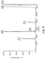
- the x-ray diffraction pattern in Figure 2 of the (100)Si/CaF2/Pd/Pt multilayer structure showed that the layers were highly oriented with an intensity ratio of Pt(200) to Pt(111) being 50:1.
- X-ray rocking curve analysis indicated that the full width at half-maximum (FWHM) of the (200) line was about 0.81°. Crystal orientation on the (100) plane was examined by x-ray diffraction at tilted planes.
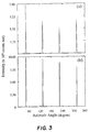
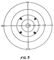
- Figure 3(a) shows an angular scan for the (220) lines of Pt when the sample was rotated around an axis parallel to its surface normal. Peaks were found every 90°, suggesting a single crystalline film. The narrow width of the peaks at half intensity of the angular scan indicated good epitaxial quality of the Pt layer.
- a (100)Si/(100)CaF2/(100)Pd/(100)Pt multilayer structure was first prepared as in Example 1.
- a zirconium precursor solution was made by refluxing a toluene solution of 1 part of zirconium n-propoxide (Alfa Chemicals) and 2 parts of neodecanoic acid, under Ar for 4.5 hours. Solvent was then removed by rotary evaporation resulting in a viscous liquid with a Zr content of 17.91 percent.
- One gram of rosin was dissolved in 2.6 grams of toluene and 1.64 grams of butyl alcohol upon heating. Then, 4.4 grams of said viscous liquid was added and gently heated for 15 minutes, cooled to room temperature and filtered with a 0.65 micron nylon membrane filter.
- the Zr content of the resulting precursor was determined by TGA to be 9.87% by weight.
- the titanium precursor was prepared by mixing Ti butoxide and excess 2-ethylhexanoic acid. The mixture was filtered, and the Ti content was determined by TGA to be 5.37% by weight.
- the PZT precursor was prepared as follows. 4.62 grams of the Zr precursor was mixed with 4.02 grams of the Ti precursor and 7.03 grams of lead resinate to produce a precursor with a composition of Pb(Zr 0.53 Ti 0.47 ).
- the lead resinate is available commercially from Engethard with a Pb content of 27.8% by weight. The mixture was heated to the boiling point, and 1.56 grams of 2-ethylhexanoic acid and 1.52 grams of rosin were added. The mixture was heated to dissolve all the rosin and was then filtered. The ratio of Pb:Zr:Ti was approximately 1:0.53:0.47 in the final precursor solution.
- the PZT precursor was spin-coated at 4000 RPM for 30 sec on the multilayer structure.
- the precursor film was heated on a hot plate up to 450°C and then thermally processed in a tube furnace at 635°C for 30 min in 10% 02/N2.
- Example 2 The same procedures were followed as in Example 2, with the exception that a KNbO3 upper layer was grown on the Pt electrode surface by pulsed laser ablation.
- the beam was focused to a 5 mm2 spot onto a target containing polycrystalline KNbO3.
- the (100)Si/(100)CaF/(100)Pd/(100)Pt multilayer structure was located 6 cm from the target and heated to 600-700°C by a resistive heater. The temperature was monitored by a thermocouple attached to an inner wall of the heater block.
- the deposition was carried out at a rate of 0.1 nm/pulse under an oxygen pressure of 106 m Torr. After 3000 pulses, the sample was cooled to room temperature with oxygen flowing at a pressure of 150 Torr.
- Example 1 The procedures of Example 1 were followed with the exception that instead of the Pd-Pt electrode, a 60 nm-thick Pd electrode was deposited on the epitaxial CaF2 buffer layer at 500°C without breaking the vacuum.
- the deposited Pd film exhibited a smooth surface and good adhesion to the CaF2 buffer layer.
- Comparative Experiments 1-6 illustrate the importance of a buffer layer between a substrate and a metal oxide upper layer.
- Comparative Experiments 7-10 indicate the importance of a single crystal buffer layer between a substrate and a metal electrode and the effect of use of a polycrystalline electrode on a superimposed metal oxide upper layer.
- a zirconium precursor solution was made by refluxing a toluene solution of 1 part of zirconium n-propoxide (Alfa Chemicals) and 2 parts of neodecanoic acid, under Ar for 4.5 hours. Solvent was then removed by rotary evaporation resulting in a viscous liquid with a Zr content of 17.91 percent.
- One gram of rosin was dissolved in 2.6 grams of toluene and 1.64 grams of butyl alcohol upon heating. Then, 4.4 grams of said viscous liquid was added and gently heated for 15 minutes, cooled to room temperature and filtered with a 0.65 micron nylon membrane filter.
- the Zr content of the resulting precursor was determined by TGA to be 9.87% by weight.
- the titanium precursor was prepared by mixing Ti butoxide and excess 2-ethylhexanoic acid. The mixture was filtered, and the Ti content was determined by TGA to be 5.37% by weight.
- the PZT precursor was prepared as follows. 4.62 grams of the Zr precursor was mixed with 4.02 grams of the Ti precursor and 7.03 grams of lead resinate to produce a precursor with a composition of Pb(Zr 0.53 Ti 0.47 ).
- the lead resinate is available commercially from Engethard with a Pb content of 27.8% by weight. The mixture was heated to the boiling point, and 1.56 grams of 2-ethylhexanoic acid and 1.52 grams of rosin were added. The mixture was heated to dissolve all the rosin and was then filtered. The ratio of Pb:Zr:Ti was approximately 1:0.53:0.47 in the final precursor solution.
- the PZT precursor was spin-coated at 4000 RPM for 30 sec on (100)Si.
- the precursor films were heated on a hot plate up to 450°C and then thermally processed in a tube furnace at 635°C for 30 min in 10% 02/N2. Interactions between Si and PZT took place during sintering. X-ray diffraction analysis indicated that the intensity of the reflection lines coming from the PZT phase was very weak and the film was randomly oriented.
- PZT precursor was prepared in the same manner as in Comparative experiment 1 and was spin-coated at 4000 RPM for 30 sec on (100)Si using an epitaxial CaF2 layer as a buffer.
- the precursor films were heated on a hot plate up to 450°C and then thermally processed in a tube furnace at 635°C for 30 min in 10% 02/N2.
- X-ray diffraction analysis showed solely the existence of (100) and (200) reflections, indicating highly oriented PZT films.
- NH4 saturated
- the wafers were divided into two sets. One set of wafers did not receive a buffer layer. CaF2 buffer layers were deposited on the other set of wafers in an electron-beam evaporator with pressures of 1 x 10 ⁇ 9 Torr prior to deposition, rising to a maximum of 1-2 x 10 ⁇ 7 Torr during deposition. No additional thermal etching was used before heating the substrates to a desired temperature for fluoride growth. The substrate was heated by a radiative heater consisting of tantalum wires. The growth temperature varied between 400-600°C and was monitored by an infrared pyrometer using published emissivity values.
- the deposition rate was 0.2-0.3 nm ⁇ sec ⁇ 1 and the thickness of the fluoride films was about 100-300 nm.
- the backside of the GaAs substrate was encapsulated with 100 nm of Si-nitride to suppress GaAs dissociation upon heating at elevated temperatures.
- PZT precursor was prepared and spin coated on both sets of wafers as in Comparative Experiment 2.
- a (100)Si wafer coated with a Pt layer was used as a base.
- the base was prepared by spin coating platinum resinate with a Pt content of 12.0% on a Si substrate and subsequently heating the substrate up to 500°C. X-ray analysis indicated that the Pt was almost randomly oriented with no signs of its reaction with Si. The limited reaction between Pt and Si is attributed to the presence of an interfacial Si-oxide layer.
- PZT precursor was prepared as in Comparative Experiment 1 and was spin-coated at 4000 RPM for 30 sec on the Pt-coated Si base. The precursor film was heated on a hot plate up to 450°C and then thermally processed in a tube furnace at 635°C for 30 minutes in 10% 02/N2. Interactions between Si and PZT were not observed, but the PZT films were randomly oriented due to the polycrystalline nature of the Pt layer.
Landscapes
- Semiconductor Lasers (AREA)
- Crystals, And After-Treatments Of Crystals (AREA)
- Optical Integrated Circuits (AREA)
- Electrodes Of Semiconductors (AREA)
Applications Claiming Priority (2)
| Application Number | Priority Date | Filing Date | Title |
|---|---|---|---|
| US992214 | 1992-12-17 | ||
| US07/992,214 US5387459A (en) | 1992-12-17 | 1992-12-17 | Multilayer structure having an epitaxial metal electrode |
Publications (2)
| Publication Number | Publication Date |
|---|---|
| EP0602532A2 true EP0602532A2 (de) | 1994-06-22 |
| EP0602532A3 EP0602532A3 (de) | 1997-07-09 |
Family
ID=25538052
Family Applications (1)
| Application Number | Title | Priority Date | Filing Date |
|---|---|---|---|
| EP93119810A Withdrawn EP0602532A3 (de) | 1992-12-17 | 1993-12-08 | Multi-Schicht Struktur mit einer epitaxialer metallischer Elektrode. |
Country Status (3)
| Country | Link |
|---|---|
| US (1) | US5387459A (de) |
| EP (1) | EP0602532A3 (de) |
| JP (1) | JPH06236988A (de) |
Cited By (5)
| Publication number | Priority date | Publication date | Assignee | Title |
|---|---|---|---|---|
| EP0667532A3 (de) * | 1994-02-07 | 1998-07-22 | Matsushita Electric Industrial Co., Ltd. | Dünnfilmm-Sensorelement sowie Verfahren zu seiner Herstellung |
| WO2018057797A1 (en) * | 2016-09-22 | 2018-03-29 | IQE, plc | Integrated epitaxial metal electrodes |
| US10418457B2 (en) | 2016-09-22 | 2019-09-17 | Iqe Plc | Metal electrode with tunable work functions |
| WO2020246995A1 (en) * | 2019-06-06 | 2020-12-10 | Iqe Plc | Integrated epitaxial metal electrodes for modified devices |
| US11495670B2 (en) | 2016-09-22 | 2022-11-08 | Iqe Plc | Integrated epitaxial metal electrodes |
Families Citing this family (26)
| Publication number | Priority date | Publication date | Assignee | Title |
|---|---|---|---|---|
| DE59309018D1 (de) * | 1992-07-02 | 1998-11-05 | Balzers Hochvakuum | Verfahren zur Herstellung einer Metalloxidschicht, Vakuumbehandlungsanlage hierfür sowie mit mindestens einer Metalloxidschicht beschichteter Teil |
| DE4323821A1 (de) * | 1993-07-15 | 1995-01-19 | Siemens Ag | Pyrodetektorelement mit orientiert aufgewachsener pyroelektrischer Schicht und Verfahren zu seiner Herstellung |
| DE69431333T2 (de) * | 1993-10-08 | 2003-07-31 | Mitsubishi Cable Industries, Ltd. | GaN-Einkristall |
| US5519235A (en) * | 1994-11-18 | 1996-05-21 | Bell Communications Research, Inc. | Polycrystalline ferroelectric capacitor heterostructure employing hybrid electrodes |
| JP3751329B2 (ja) * | 1994-12-06 | 2006-03-01 | コマツ電子金属株式会社 | エピタキシャルウェーハの製造方法 |
| JPH11511293A (ja) * | 1995-06-07 | 1999-09-28 | サイメトリックス コーポレイション | 基板および配線層を備え、基板と配線層との間にバッファ層を有する集積回路 |
| US5785756A (en) * | 1997-03-06 | 1998-07-28 | Northrop Grumman Corporation | Process for fabricating structurally robust optical coatings |
| US7035880B1 (en) | 1999-07-14 | 2006-04-25 | Commvault Systems, Inc. | Modular backup and retrieval system used in conjunction with a storage area network |
| US7395282B1 (en) * | 1999-07-15 | 2008-07-01 | Commvault Systems, Inc. | Hierarchical backup and retrieval system |
| US6214712B1 (en) * | 1999-09-16 | 2001-04-10 | Ut-Battelle, Llc | Method of physical vapor deposition of metal oxides on semiconductors |
| US7003641B2 (en) | 2000-01-31 | 2006-02-21 | Commvault Systems, Inc. | Logical view with granular access to exchange data managed by a modular data and storage management system |
| US6658436B2 (en) | 2000-01-31 | 2003-12-02 | Commvault Systems, Inc. | Logical view and access to data managed by a modular data and storage management system |
| JP3514207B2 (ja) * | 2000-03-15 | 2004-03-31 | 株式会社村田製作所 | 強誘電体薄膜素子ならびにセンサ、および強誘電体薄膜素子の製造方法 |
| US6465887B1 (en) * | 2000-05-03 | 2002-10-15 | The United States Of America As Represented By The Secretary Of The Navy | Electronic devices with diffusion barrier and process for making same |
| JP3971598B2 (ja) * | 2001-11-01 | 2007-09-05 | 富士通株式会社 | 強誘電体キャパシタおよび半導体装置 |
| JP4118061B2 (ja) * | 2002-02-07 | 2008-07-16 | 三洋電機株式会社 | 半導体の形成方法および半導体素子 |
| JP2004095638A (ja) * | 2002-08-29 | 2004-03-25 | Fujitsu Ltd | 薄膜デカップリングキャパシタとその製造方法 |
| US7454569B2 (en) | 2003-06-25 | 2008-11-18 | Commvault Systems, Inc. | Hierarchical system and method for performing storage operations in a computer network |
| US7546324B2 (en) | 2003-11-13 | 2009-06-09 | Commvault Systems, Inc. | Systems and methods for performing storage operations using network attached storage |
| JP4101823B2 (ja) * | 2005-06-13 | 2008-06-18 | 株式会社東芝 | 半導体素子、電極形成方法及び半導体素子の製造方法 |
| TWI387417B (zh) * | 2008-08-29 | 2013-02-21 | Ind Tech Res Inst | 電路板結構及其製作方法 |
| US8766341B2 (en) * | 2009-10-20 | 2014-07-01 | The Regents Of The University Of California | Epitaxial growth of single crystalline MgO on germanium |
| US9021198B1 (en) | 2011-01-20 | 2015-04-28 | Commvault Systems, Inc. | System and method for sharing SAN storage |
| EP2656912A1 (de) * | 2012-04-26 | 2013-10-30 | Saudi Basic Industries Corporation | Photokatalysator, Herstellungsverfahren, Photolysesystem |
| KR101414205B1 (ko) * | 2013-09-30 | 2014-07-01 | 주식회사 엘지실트론 | 웨이퍼의 기계적 손상 깊이를 측정하는 방법 |
| CN121496343B (zh) * | 2026-01-14 | 2026-04-17 | 宁波锦辉光学科技股份有限公司 | 一种光学薄膜应力控制方法及真空镀膜系统 |
Family Cites Families (6)
| Publication number | Priority date | Publication date | Assignee | Title |
|---|---|---|---|---|
| DE2824870A1 (de) * | 1978-06-07 | 1979-12-20 | Philips Patentverwaltung | Verfahren zur herstellung eines dielektrikums mit perowskitstruktur |
| JPS5817651A (ja) * | 1981-07-24 | 1983-02-01 | Hitachi Ltd | 多層回路板とその製造方法 |
| EP0544399A3 (en) * | 1991-11-26 | 1993-10-27 | Xerox Corp | Epitaxial magnesium oxide as a buffer layer for formation of subsequent layers on tetrahedral semiconductors |
| US5155658A (en) * | 1992-03-05 | 1992-10-13 | Bell Communications Research, Inc. | Crystallographically aligned ferroelectric films usable in memories and method of crystallographically aligning perovskite films |
| US5270298A (en) * | 1992-03-05 | 1993-12-14 | Bell Communications Research, Inc. | Cubic metal oxide thin film epitaxially grown on silicon |
| US5248564A (en) * | 1992-12-09 | 1993-09-28 | Bell Communications Research, Inc. | C-axis perovskite thin films grown on silicon dioxide |
-
1992
- 1992-12-17 US US07/992,214 patent/US5387459A/en not_active Expired - Fee Related
-
1993
- 1993-12-08 EP EP93119810A patent/EP0602532A3/de not_active Withdrawn
- 1993-12-13 JP JP5312318A patent/JPH06236988A/ja active Pending
Cited By (10)
| Publication number | Priority date | Publication date | Assignee | Title |
|---|---|---|---|---|
| EP0667532A3 (de) * | 1994-02-07 | 1998-07-22 | Matsushita Electric Industrial Co., Ltd. | Dünnfilmm-Sensorelement sowie Verfahren zu seiner Herstellung |
| US6105225A (en) * | 1994-02-07 | 2000-08-22 | Matsushita Electric Industrial Co., Ltd. | Method of manufacturing a thin film sensor element |
| WO2018057797A1 (en) * | 2016-09-22 | 2018-03-29 | IQE, plc | Integrated epitaxial metal electrodes |
| US10128350B2 (en) | 2016-09-22 | 2018-11-13 | Iqe Plc | Integrated epitaxial metal electrodes |
| CN109964302A (zh) * | 2016-09-22 | 2019-07-02 | Iqe公司 | 集成的外延金属电极 |
| US10418457B2 (en) | 2016-09-22 | 2019-09-17 | Iqe Plc | Metal electrode with tunable work functions |
| US10825912B2 (en) | 2016-09-22 | 2020-11-03 | Iqe Plc | Integrated epitaxial metal electrodes |
| TWI764930B (zh) * | 2016-09-22 | 2022-05-21 | 英商Iqe有限公司 | 集成外延金屬電極 |
| US11495670B2 (en) | 2016-09-22 | 2022-11-08 | Iqe Plc | Integrated epitaxial metal electrodes |
| WO2020246995A1 (en) * | 2019-06-06 | 2020-12-10 | Iqe Plc | Integrated epitaxial metal electrodes for modified devices |
Also Published As
| Publication number | Publication date |
|---|---|
| JPH06236988A (ja) | 1994-08-23 |
| EP0602532A3 (de) | 1997-07-09 |
| US5387459A (en) | 1995-02-07 |
Similar Documents
| Publication | Publication Date | Title |
|---|---|---|
| EP0602532A2 (de) | Multi-Schicht Struktur mit einer epitaxialer metallischer Elektrode | |
| US5912068A (en) | Epitaxial oxides on amorphous SiO2 on single crystal silicon | |
| US5919515A (en) | Ferroelectric thin film, electric device and method for preparing ferroelectric thin film | |
| EP0661754B1 (de) | Struktur, die eine dünne Schicht aus einem ferroelektrischen Kristall enthält, Verfahren zur Herstellung und diese Struktur verwendende Vorrichtung | |
| US6756139B2 (en) | Buffer layers on metal alloy substrates for superconducting tapes | |
| US5801105A (en) | Multilayer thin film, substrate for electronic device, electronic device, and preparation of multilayer oxide thin film | |
| EP0747937B1 (de) | Verfahren zur Herstellung eines mit einer dünnen ferroelektrischen Schicht überdeckten Substrats | |
| US5470668A (en) | Metal oxide films on metal | |
| US6143366A (en) | High-pressure process for crystallization of ceramic films at low temperatures | |
| JP3436617B2 (ja) | 強誘電体薄膜の製造方法 | |
| US5241191A (en) | Cubic perovskite crystal structure, a process of preparing the crystal structure, and articles constructed from the crystal structure | |
| EP0747938B1 (de) | Mit einer dünnen ferreoelektrischen Schicht überdecktes Substrat, Verfahren zu seiner Herstellung und in diesem verwendende Kondensator-Struktur | |
| Kijima et al. | New Low-Temperature Processing of Metalorganic Chemical Vapor Deposition-Bi4Ti3O12 Thin Films Using BiO x Buffer Layer | |
| Theis et al. | Epitaxial lead titanate grown by MBE | |
| US7129196B2 (en) | Buffer layer for thin film structures | |
| WO1996030938A2 (en) | Process for fabricating layered superlattice materials and making electronic devices including same | |
| JPH0967193A (ja) | 強誘電体薄膜の製造方法 | |
| US4874741A (en) | Non-enhanced laser evaporation of oxide superconductors | |
| US6531235B2 (en) | Non-c-axis oriented bismuth-layered perovskite ferroelectric structure epitaxially grown on buffered silicon | |
| Mansingh et al. | Preparation and properties of thermally evaporated lead germanate films | |
| Roy et al. | Substrate and temperature effects in lead zirconate titanate films produced by facing targets sputtering | |
| US5552373A (en) | Josephson junction device comprising high critical temperature crystalline copper superconductive layers | |
| JP2834355B2 (ja) | 強誘電体薄膜構成体の製造方法 | |
| Blednov et al. | Epitaxial calcium and strontium fluoride films on highly mismatched oxide and metal substrates by MOCVD: Texture and morphology | |
| Yanase et al. | Epitaxial Growth of Ti1-xAl xN Buffer Layer for a Ferroelectric (Ba, Sr) TiO3 Capacitor on Si Substrate |
Legal Events
| Date | Code | Title | Description |
|---|---|---|---|
| PUAI | Public reference made under article 153(3) epc to a published international application that has entered the european phase |
Free format text: ORIGINAL CODE: 0009012 |
|
| AK | Designated contracting states |
Kind code of ref document: A2 Designated state(s): DE FR GB |
|
| PUAL | Search report despatched |
Free format text: ORIGINAL CODE: 0009013 |
|
| AK | Designated contracting states |
Kind code of ref document: A3 Designated state(s): DE FR GB |
|
| 17P | Request for examination filed |
Effective date: 19980108 |
|
| 17Q | First examination report despatched |
Effective date: 20000218 |
|
| STAA | Information on the status of an ep patent application or granted ep patent |
Free format text: STATUS: THE APPLICATION IS DEEMED TO BE WITHDRAWN |
|
| 18D | Application deemed to be withdrawn |
Effective date: 20000629 |